
 Open Access Article
 This Open Access Article is licensed under a
 Creative Commons Attribution 3.0 Unported Licence
Band gap opening and semiconductor–metal phase transition in (n, n) single-walled carbon nanotubes with distinctive boron–nitrogen line defect†
Ming
Qiu
ab,
Yuanyuan
Xie
a,
Xianfeng
Gao
a,
Jianyang
Li
a,
Yelin
Deng
a,
Dongsheng
Guan
a,
Lulu
Ma
a and
Chris
Yuan
*a
aDepartment of Mechanical Engineering, University of Wisconsin Milwaukee, Wisconsin 53211, USA. E-mail: cyuan@uwm.edu
bSchool of Physics and Electronic Science, Changsha University of Science and Technology, Changsha 410114, China
First published on 18th January 2016
Abstract
Band gap opening and modulating are critical in dictating the functionalities of single walled carbon nanotubes (SWCNTs) in a broad array of nano-devices. Using first-principles density functional theory calculations, a class of semiconducting armchair SWCNTs with a distinctive BN line defect are studied, showing a super capacity to open the band gap of (4, 4) SWCNT to as large as 0.86 eV, while the opened band gap are found decreasing with the increasing diameters of SWCNTs. The opened band gap of SWCNTs can also be successfully modulated through both mechanical and electrical approaches by applying compressive uniaxial strain and electric field. This study provides novel insights into the large band gap opening and modulating of SWCNTs and could be useful in facilitating future applications of SWCNTs in electronic, optical and thermoelectric devices.
1 Introduction
With such superior properties as high carrier mobility, high thermal conductivity, high tensile strength, high Young's modulus and hollow structure etc., single-walled carbon nanotubes (SWCNTs)1,2 have found a wide range of applications on a number of functional devices including chemical sensors,3,4 electrochemical devices,5,6 hydrogen storage devices,7,8 field emission devices9,10 and nanoscale electronic devices,11,12etc. In general, these devices employ different material behaviors of SWCNTs ranging from metallic to semimetallic to semiconducting, as simply characterized by their increasing electronic band gap.13,14 It was Deshpande et al.15 who first found in their experiments that the metallic armchair SWCNTs have a band gap of 0.01–0.10 eV which could be potentially tuned to display different material properties from metallic to semiconducting on the same SWCNTs. This interesting finding has attracted enormous interests in recent years in opening the band gaps of metallic SWCNTs to obtain a tunable and applicable metallic-semiconducting molecular devices. To open the band gaps of metallic SWCNTs, two distinct strategies are typically adopted: internal or external feature approaches. The internal feature approach relies on modifying the SWCNT structure or inducing internal property change to open the band gap.15–21 For example, with a corrugated structure, the band gaps of (3, 3) and (4, 4) SWCNTs could be opened to 0.280 and 0.095 eV, respectively;16 with a phonon distortion, the band gap of a (3, 3) SWCNT can be opened to 0.25 eV;17,18 with a bond rotation defect, the band gap of a (9, 0) zigzag SWCNT can be opened to about 0.50 eV,19 and with a BN domain, the band gap of a (15, 0) zigzag SWCNT can be opened to 0.39 eV.20 In contrast, the external feature approach takes advantages of external factors in opening the band gap of SWCNTs.22–27 For instance, the tube–tube interactions in ropes of armchair SWCNTs can separate their conduction and valence bands by a gap of about 0.1 eV;22–24 the vanadium atomic chain adsorbed on the outer surface of SWCNTs can strongly influence the electronic structure of the (6, 6) and (8, 8) metallic armchair SWCNTs and can open their band gaps to 0.49 eV;25 a supporting silicon substrate under the SWCNTs has been found to be able to enlarge the band gap of a small armchair (3, 3) SWCNT to about 0.11 eV.26,27After opening, the band gap of the SWCNT also needs to be continuously modulated to achieve precise phase transition between metallic and semiconducting properties which can greatly help to improve the device performance and expand its functionalities and applications.28–31 For this purpose, a number of experimental techniques and theoretical methods have been developed in recent years. For instance, with metallofullerenes inserted, the SWCNTs can act as multiple quantum dots;32 with bimolecular decoration, they can achieve metal–semiconductor transition33 and detect DNA hybridization34 and conformational polymorphism;35 with electrical,36–38 mechanical39,40 and magnetic approaches,41 their band gaps can be modulated for potential applications in molecular devices. Among these available techniques, the mechanical and electrical approaches are most widely investigated, and the modulated devices are explored extensively as one of the most promising alternatives to the silicon-based electronic components. For mechanical modulating, a twisted armchair SWCNT has been found to show insulator-like conductivity through atomically resolved scanning tunneling microscopy images.42 Mechanical squashing can lead to the conductance oscillations43,44 and metal-to-semiconductor transition45,46 in armchair SWCNT. For electrical modulating, the SWCNT shows a significantly increased current density (exceeding 109 A cm−2),47 Majorana bound states48 and band gap modulation49–51 under the electrical field as induced by dramatic scattering of electrons, proximity effect and axial polarization.
However, finding more CNT-based functional devices and tuning their characteristics to understand the fundamental physical mechanism and improve their performance are still remaining challenges. A particular question is whether a new class of CNTs can be constructed from graphene nanoribbons (GNRs), via Klein edges of GNRs.52–56 He et al.57 validated experimentally that the edges of GNRs can be transformed to form extended symmetric Klein edges which can be maintained stably for 2s before further structural transformation occurs. Meanwhile, the carbon atoms of the Klein defect can be replaced by groups,58,59 metal60 and non-metal atoms.61–64 Interestingly, Šljivančanin65 found the hydrogenated CNTs (5, 5) have similar properties with 10-zigzag GNR (ZGNR). Lee et al.66 investigated the half metallicity of hydrogenated CNT (8, 8) and found it is similar with 16-ZGNR.67 Du et al.14 fabricated BNC nanotubes from the BN and C domains. The above results illustrate that it is possible to roll up the edge-modified GNRs to build a new class of SWCNTs which could pave a new way to extend the families of carbon-based materials and demonstrate more interesting functionality and applicability for future molecular devices.
Obviously, connecting the two modified edges of GNR can introduce certain domains. These defects can break the structural symmetry and change the electronic structures which could help open the band gap of new built CNTs. While significant efforts have been made recently on band gap opening and continuous modulating of SWCNTs, the best result reported in literature on band gap opening of SWCNTs is only 0.50 eV.19 In this paper, we predict a new class of semiconducting armchair SWCNT and successfully obtained a large band gap opening with a distinctive BN line defect, using both mechanical and electrical modulating for a precise control of the semiconductor–metal phase transition. We also propose a new method to break the structural symmetry of the armchair SWCNT which the dipole moments induced by the BN defect can take the key place to enhance the device performance. First-principles density functional theory (DFT) is used for the simulation. The fundamental mechanism for the large band gap opening and modulating are explained and reported in details.
2 Methods and structures
In this study, first-principles DFT is employed to calculate the band gap opening and modulating of armchair SWCNT, based on a supercell configuration using the Atomistix Toolkit (ATK).68,69 As shown in Fig. 1, the armchair SWCNT with BN line defect is constructed from a zigzag graphene nanoribbon (ZGNR) with B and N terminations each on one side which also can be understood as the heterostructure consisting of BN single-walled nanotube70–72 and graphene. In the calculation, the generalized gradient approximation (GGA) within Perdew–Burke–Ernzerhof (PBE) form73 is used as the exchange–correlation function. It has been reported that DFT-PBE calculations can underestimate the band gaps of many materials, but for CNTs, graphene and BNC nanostructures, it can describe the band structure and trend properly and correctly.74–76 Norm-conserving pseudo-potentials are employed to represent the atomic core and double ζ plus double polarization basis sets to expand the valence states of electrons. In the calculation, the mesh cutoff is set at 200 Hartree, with a 1 × 1 × 33 K-point grid. In the supercell configuration, a sufficiently large separation (about 20 Å) between adjacent SWCNTs and ZGNRs is maintained. In order to minimize the perturbation from the internal force and to better understand the ground state properties, the geometries of the supercells, including the ZGNRs and SWCNTs, are optimized through Quasi-Newton method until all residual forces on each atom are smaller than 0.005 eV Å−1 and the maximum stress along the z direction of the supercell is smaller than 0.005 eV Å−3.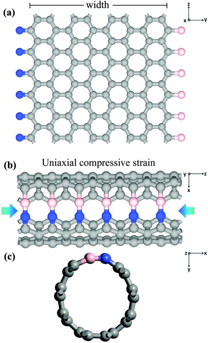 | ||
| Fig. 1 (a) Model geometry of (4, 4) ZGNR terminated with Boron (color pink) and Nitrogen (color blue) atoms each on one side. (b) Model geometry of (4, 4) armchair SWCNT with B–N line defect. (c) The side-view of (4, 4) armchair SWCNT with B–N line defect. | ||
In the DFT calculations, the formation energy denoting the energy transfer from bn@ZGNR to bn@CNT, is calculated through:
| Eform = Ebn@CNT − Ebn@ZGNR | (1) |
 | (2) |
 | (3) |
| Hμv(k)Ψn,μv(k) = En(k)SμvΨn,μv(k) | (4) |
| m* = ℏ2[d2En(k)/dk2]−1 | (5) |
| vg = P/m* = ℏk/m* | (6) |
Development of such armchair SWCNTs with a distinctive BN line defect is possible from experimental perspective. Previous experimental results have shown that the atomic layers of h-BNC71 and BNC nanotubes77 can be deposited on the Cu and Ni–Fe-coated SiO2/Si substrates. The BN and C domains show energetically stable to form the heterostuctures.14 Similarly, the graphene nanostructure terminated with B or N has been reported.64 Accordingly, like the reported work,14,65,66 it is possible to construct new GNR and SWCNT with metal or non-metal line defects. To validate this idea, we first build two ZGNRs that one is terminated with B and H each on one side, and the other has N and H terminations each on one side. Using CASTEP, we reduce the distance of B and N sides of two ZGNRs and perform a molecular dynamics simulation. The molecular dynamics results show that the two ZGNRs can be connected to form a new ZGNR with BN line defect. Then, we construct a ZGNR with B and N each on one side and wrap this ZGNR to reduce the distance of B and N to about 3.7 Å (about corresponding B and N atoms can bond side-to-side to form a 3 times of the length of BN bond). The results show that the corresponding B and N atoms can bond side-to-side to form a new BNC heterostructure, bn@CNT (Mov. S1, ESI†), to finally obtain the SWCNT with BN line defect.
As shown in Fig. 1(a) and (b), a (4, 4) bn@CNT was fabricated following above procedure using the (4, 4) bn@ZGNR whose corresponding B and N atoms were side-to-side connected to form the distinctive B–N line defect. The new (4, 4) bn@CNT is referred to as 4bn@CNT. In the formula, the number 4 represents the width of bn@ZGNR from which the 4bn@CNT is fabricated. After the BN line defect being developed, the structural symmetry of the SWCNT has been changed, so in this paper the width of bn@ZGNR is used to represent the diameter of corresponding bn@CNT. In this heterostructure, N has an electronegativity78 larger than B and C, χ(N) = 3.04 > χ(C) = 2.55 > χ(B) = 2.04; therefore, electrons can move from B to C and to N. For B- or N-terminated ZGNRs, the N-terminated edge-states are charged with transferred electrons from neighboring C atoms, while B-terminated edge-states are creating holes by losing electrons to neighboring C atoms. Then, the edge-states of ZGNRs with B- or N-terminated are delocalized,64,79 and the ZGNRs with B and N attached on each edge are strongly metallic (Fig. S1, ESI†) because of the asymmetrical delocalized edge-states on each side.
3 Results and discussion
3.1 Gap opening
The evolution in band gap energy of bn@CNTs with different widths from 4 to 24 is calculated and presented in Fig. 2; the inset is the dipole moment of bn@CNTs along the z axis with widths from 4 to 24. The width-dependent formation energy indicates that it is an exothermic fabrication process from bn@ZGNR to bn@CNT, and the formation energy is found decreasing with the increasing width, as shown in Fig. S2 (ESI†). The results in Fig. 2 illustrates that the band gap of SWCNTs has been opened obviously, while the opened gap decreases with the increasing width. As shown in Fig. 2, the DFT calculated band gap opening of bn@CNTs with widths of 4, 8, 12, 16, 20 and 24 are 0.86, 0.60, 0.46, 0.35, 0.27 and 0.24 eV, respectively. To the best of our knowledge, the band gap opening of small CNT (i.e. 4bn@CNT) to 0.86 eV, is the largest gap opening ever reported in literature.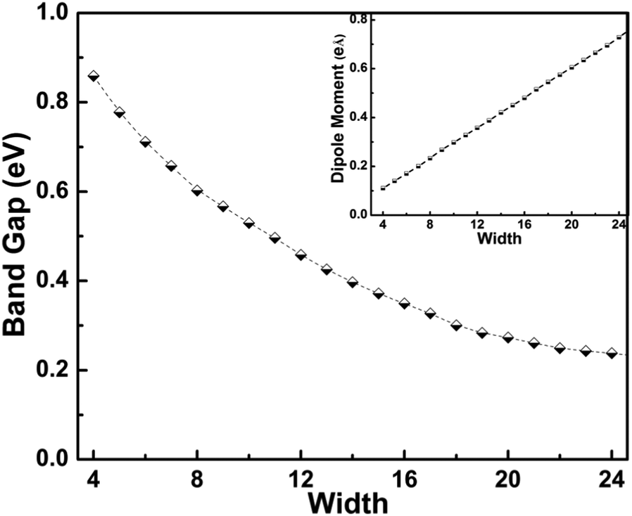 | ||
| Fig. 2 The evolution in band gap energy of bn@CNTs with different widths from 4 to 24. The inset is the dipole moment along the z axis with the widths from 4 to 24. | ||
The first reason for this large band gap opening is the different bond energies which separates the bn@CNT into two domains: the BC2N (the BN and their first neighboring carbon atoms) and C (other carbon atoms) domains. On bn@CNT, the calculated average lengths of B–C, B–N and C–N bonds are 1.49, 1.29 and 1.33 Å, respectively, which are shorter than those (1.52, 1.45 and 1.39 Å, respectively) of the single layer of h-BNC.80 With an inverse relationship between bond length and bond energy, the B–C, B–N and C–N bonds show higher bond energies than those on the single layer of h-BNC. Especially for the B–N bond, the bond length is reduced more than 11%. Due to the ionic nature, it undoubtedly has higher bond energy and can enhance the tendency to segregate the BC2N and C domains. From the Mülliken population analysis, although the B (N) on the bn@CNTs donates (accepts) about 150% more electrons than the B (N) on the bn@ZGNRs, the BN line defect contributes about 0.02e to the neighboring carbon atoms. Simply, the N and neighboring C atoms take most of B's p electrons away. That is why its electron density (Fig. S3, ESI†) changes and affects the transport eigen-channels on the bn@CNT.
The second reason for the large band gap opening is that the structural mirror asymmetry of bn@CNT, as induced by the BN line defect, not only leads to two different domains, but also introduces three permanent dipole moments. First, the charge asymmetry distribution on the BN line defect has a local dipole moment (along the x axis), and the two asymmetric hybridized states on the two C atoms of B–C and N–C bonds form a small dipole moments counteract with each other and reduce the total dipole moment reversed to the B–N direction. But these two dipole moment along the x axis. Second, the BC2N domain forms a coulomb dipole moment (along the y axis) with the carbon atoms on the cross-section ring. But from our Mülliken population analysis, the BN line defect denotes only a little charge (about 0.02e) to the C carbon atoms which does not contribute much to the gap opening. Third, the BN line defect yields a bond dipole moment along the z axis which is induced jointly by the hybridization and asymmetrical distribution of BN states. Based on our calculations, the BN bond in the bn@CNT is shortened with the increasing of width (Fig. S4, ESI†). The shortened BN bond enhances the hybridization of BN states, and directly induces the increasing of the bond dipole moment with width along the z axis (Fig. 2). With such moments, the structural symmetry of pristine SWCNT is broken, and a gap is then opened and π–π* hybridization follows.
As calculated, the bn@CNTs gap opening decrease from 0.86 eV to 0.24 eV with the increasing width from 4 to 24. The results are shown in Fig. 2, which is in good agreement with the linear dependence of the effective mass and tube diameter as reported before.81 The calculated band structures of bn@CNTs with different widths of 4, 8, 12 and 16 are presented in Fig. 3. From this figure, the opened bn@CNTs with small widths 4 and 8, are indirect band gap semiconductors with the highest occupied molecular orbital (HOMO) located at Γ point and lowest unoccupied molecular orbital (LUMO) located at K point. This clearly indicates that the BN line defect has significant effect on breaking the symmetry of small bn@CNTs. With the increasing of the bn@CNT diameter, the shortened B–N bond (Fig. S4, ESI†) increases the hybridization of the BN line defect and dipole moments along the z axis. The opened large bn@CNTs with widths 12 and 16 become direct band gap semiconductors with HOMO and LUMO both located at K point. When the tube diameter approaches infinity, the band structure of bn@CNT is close to that of pristine armchair SWCNTs added with BN states which is the band structure located near the Γ point. From the projected density of states (Fig. S5, ESI†), the HOMO consists of three states (B, C and N atoms), while the LUMO is mostly built on C atoms. Combined with the band structure, the density of states of valance band consists of two parts: the states near the Γ point distributing mostly on the BN line defect (more on N atom) and the states near the Dirac point spreading on the C atoms. The conduction band consists of states on the carbon atoms. From our calculation, the states of the conduction band mostly come from the C atoms near the B atom. The valance band is consisting of 2p orbitals of C and 2p hybrid states of BN, while the conduction band is mostly composed of the states on C atoms. For large width bn@CNTs, the states of 2p orbital of C atoms take more weight and come closer to the Fermi level than the hybrid states of BN. As a result, the bn@CNT becomes the direct band gap.
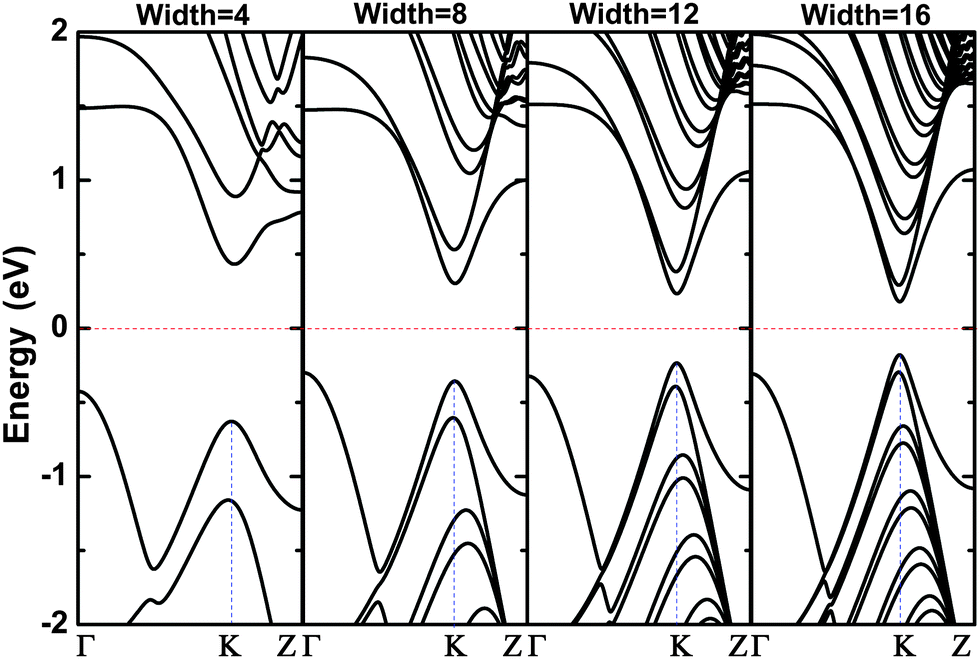 | ||
| Fig. 3 The band structures of bn@CNTs with different widths 4, 8, 12 and 16. | ||
3.2 Mechanical modulating of opened band gaps
In this section, the mechanical modulating of opened band gap is simulated under uniaxial compressive strain, as shown in Fig. 4 for different widths 4, 8, 12, 16, 20 and 24. The applied compressive strain is in the range of 0–3% of the z-axis lattice length. From Fig. 4, the electronic structure of bn@CNT is found sensitive to the uniaxial compressive deformation. The band gaps of all studied bn@CNTs decrease in a linear relationship with increasing compressive strain except the 12bn@CNT and 16bn@CNT, which change slightly during 0–1% strain level. From the results, applying 3% compressive strain can reduce the band gap of 4bn@CNT from 0.86 eV to 0.49 eV, while reduce the band gap of 20bn@CNT from 0.27 eV to 0.01 eV. For the 12bn@CNT and 16bn@CNT, the band gaps begin to decrease rapidly from 0.8% and 1.2% strain, respectively. In summary, the 3% compressive strain can transfer the 20bn@CNT and 24bn@CNT from semiconductor to metal; with the increasing of the compressive strain, the 4bn@CNT, 8bn@CNT, 12bn@CNT and 16bn@CNT will undergo certain phase transitions as well.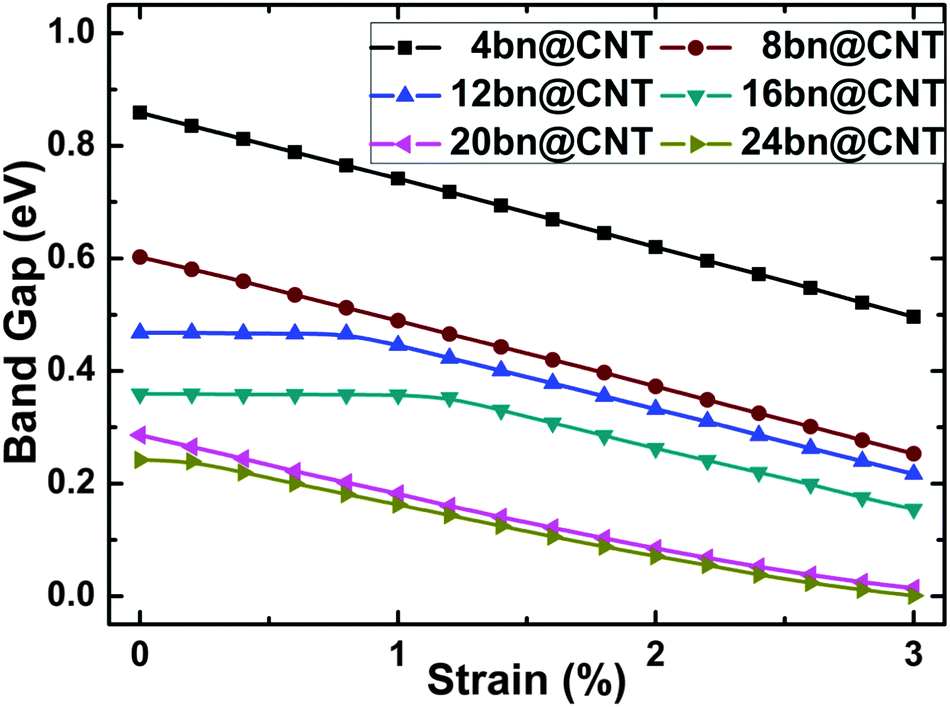 | ||
| Fig. 4 The variation in band gaps of bn@CNTs with different widths 4, 8, 12, 16, 20 and 24 under the uniaxial compressive strain. | ||
The band structures of 4bn@CNT and 12bn@CNT under different uniaxial compressive strains are calculated and presented in Fig. 5. As known from the simple bond rule, B–N bonds are stronger than the B–C and C–N bonds. When the uniaxial compressive strain is applied, the B–C and C–N bonds are lengthened while the B–N bond and first C–C bonds adjacent to the B–C and C–N bonds on the bn@CNT are gradually shortened. Electrons transferred from B atom to its neighboring N and C atoms are accordingly reduced. As a result, the dipole moment along the y axis decreases (Fig. S6, ESI†), while the dipole moments along the x and z axes increase slightly. In this way, the charges are redistributed, and the effect of the dipole moment on the polarization is reduced. From Fig. 5(a) and (b), this redistribution also leads to the moving of the HOMO and LUMO close to the Fermi level, as the strain increases (Fig. S7, ESI†). From the calculations, the chemical potential shifts up-ward with the increasing of strain. For 12bn@CNT and 16bn@CNT, they have direct band gaps in the ground state. However, under the compressive deformation, the states on the Γ point, mostly composed of the states on the BN line defect (Fig. S8, ESI†), shift faster up-ward to approach the Fermi level than that on the K point. With the increasing strain, they pass the states on the K point and change the gaps of 12bn@CNT and 16bn@CNT from direct to indirect band gaps. In this way, the different sensitivity of states and the continuous change of bond length, charge redistribution and dipole moment all contribute to the mechanical modulating of the opened band gap.
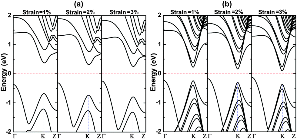 | ||
| Fig. 5 The band structures of (a) 4bn@CNT and (b) 12bn@CNT under different uniaxial compressive strain. | ||
For comparison, the electronic properties of the bn@CNTs under uniaxial elastic strain is also calculated and it is found that, under 5% elastic strain, the band gaps are widened 26.5%, 11.9%, 2.4% and 1.1% for 4bn@CNT, 8bn@CNT, 12bn@CNT and 16bn@CNT, respectively. Interestingly, the band structures show that the bn@CNTs are semiconductors with direct band gaps under elastic strain, which indicates that the states on the K point are more sensitive to elastic strain than those on the Γ point. This means the BN line defect is more sensitive to the compressive strain, while the C atoms are more sensitive to the elastic strain.
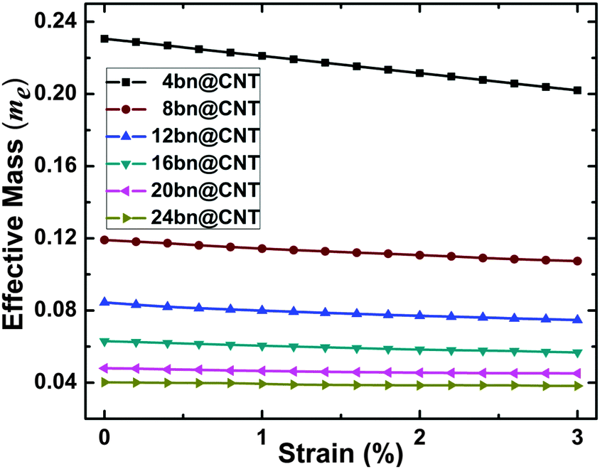
For device application, the evolution of effective electron mass (in units of the free electron mass me) with different widths under the compressive strain is calculated and presented in Fig. 6. The width- and strain-dependent effective electron mass is found decreasing linearly with uniaxial compressive strain. Nevertheless, the decreasing trend is diminishing with the increasing of widths from 4 to 24. From the results, the effective electron mass of 4bn@CNT, 12bn@CNT and 20bn@CNT decreases by 12%, 11% and 6% from 0.230 me to 0.202 me, 0.084 me to 0.075 me, and 0.048 me to 0.045 me respectively, under 3% uniaxial compressive strain. Because of the inverse relationship between mass and velocity, it shows that the carrier mobility of bn@CNT can be effectively tuned by uniaxial compressive deformation.
 | ||
| Fig. 6 The evolutions of effective electron mass (in units of the free electron mass me) with different widths under uniaxial compressive strain. | ||
3.3 Electrical modulating of opened band gaps
In this section, the electrical modulating of opened band gap is computed between −0.10 to +0.10 V Å−1. The modulated band gap results are calculated and presented in Fig. 7. Our DFT calculations indicate that the large bn@CNTs are more sensitive to the applied electric field modulating. Fig. 7 shows the modulated band gaps for different widths 16, 20 and 24. From this figure, the band gaps of large bn@CNTs can be effectively modulated by both positive and negative electric field applied along the y axis. Benchmarking between the three different widths of opened bn@CNTs, the 24@CNT is most sensitive to the applied electric field and is the most quickly approaching metallic under the same electric field. Under a electric field of −0.10 (0.10) V Å−1, the band gap of 16bn@CNT decreases from 0.36 to 0.02 (0.05) eV, while for 24bn@CNT, a small field of −0.04 (0.04) V Å−1 can reduce its band gap from 0.24 to 0.02 (0.03) eV. Nevertheless, those small diameter bn@CNTs are slightly resistive to the applied electric field. Our calculated results show that the band gaps of 4bn@CNT and 8bn@CNT will decrease. For comparison, the electrical modulating of band gaps of bn@CNTs under electric field applied along the x axis are also calculated and shown in Fig. S9 (ESI†). They all have similar switching behaviors, while the modulating is more sensitive to the electric field applied along the y axis.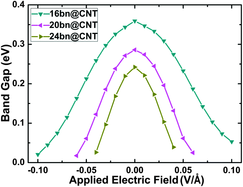 | ||
| Fig. 7 The variation in band gaps of bn@CNTs with different widths 16, 20 and 24 under electric field applied along the y axis. | ||
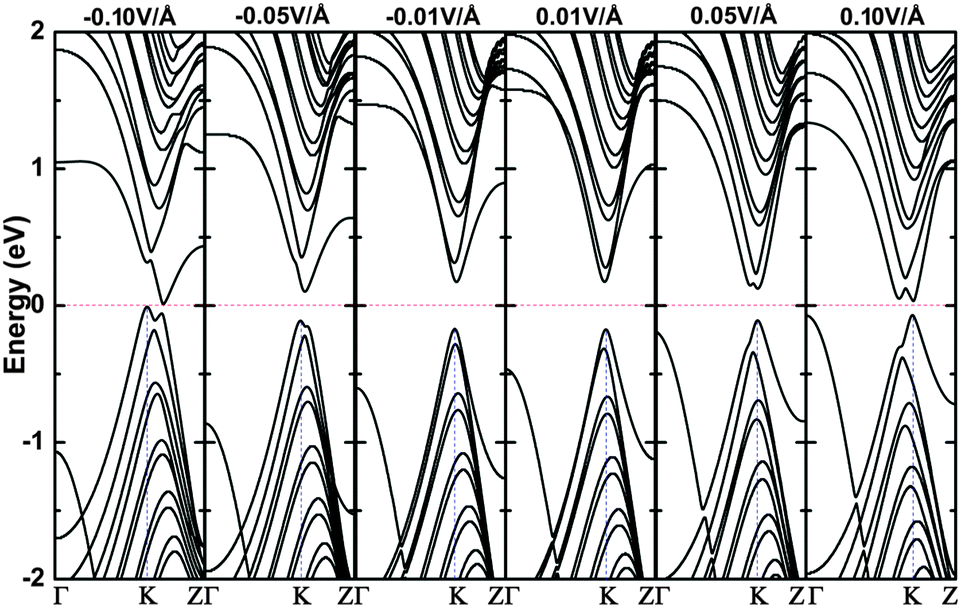
As an example, the 16bn@CNT is used to explain the field-effect behavior under the electrical modulating, and the modulated band structures under electric fields applied along the y axis are shown in Fig. 8. From this figure, the band gap decreases quickly with the increasing of electric field. From the electric fields of 0.05 (−0.05) to 0.10 (−0.10) V Å−1, the states near the minimum of conduction band (maximum of valance band) show a degeneracy of the states, and the states on the Γ point shift up (down) slightly. The positive applied electric field keeps the direct band gaps of 16bn@CNT, while the negative electric field switches it to indirect band gaps. From the figure, the LUMO moves away from the Fermi level only at an electric field of 0.01 and 0.02 V Å−1. Then, the LUMO shifts downward and is moving closer to the Fermi level at an electric field of −0.10 V Å−1 than that at 0.10 V Å−1. The HOMO shifts upward to the Fermi level, while it moves faster under the positive electric field. For further investigation, the eigenstates from the MPSH calculations at the electric fields of 0, ±0.01 and ±0.10 V Å−1 are shown in Fig. S10 (ESI†). The HOMOs always locate at the BN line defect and partially at the C atom neighboring N atom. The LUMO distributes mostly on the top area, at the BN line defect and their neighboring C atoms under the negative and low positive electric field (0.01 V Å−1). But under an electric field of 0.10 V Å−1, the LUMO locates on the bottom area. From our projected density of states calculation, the states near the Fermi level are mostly composed of the 2p orbitals of BN line defect and their neighboring C atoms (the C atoms near the bottom) under a gate voltage of −0.10 (0.10) V Å−1, which also agrees well with our calculated MPSH results as described above. As found, the increasing electric fields change the effective work functions and decrease the HOMO–LUMO gap of 16bn@CNT. From Fig. 8, the degenerate states shift towards the Fermi level and split to nondegenerate under high applied voltages induced by the increase of the coulomb repulsion near the Fermi level.
 | ||
| Fig. 8 The band structures of 16bn@CNT under different electric fields along the y axis. | ||
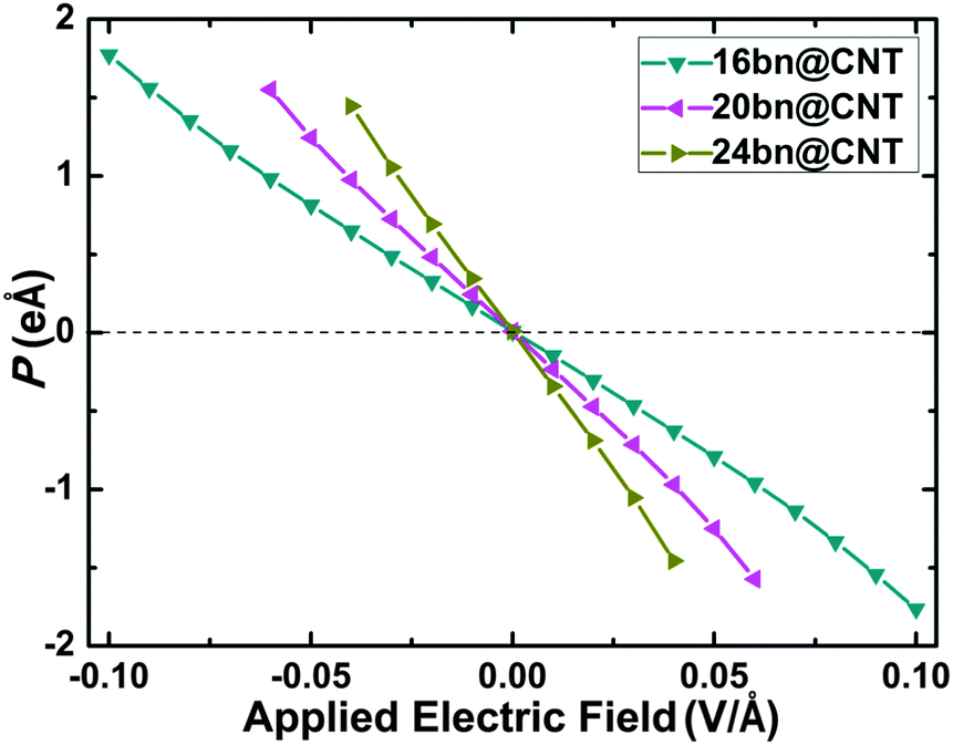
To further investigate the modulating behavior, the evolutions of dipole moments for different widths 16, 20 and 24 bn@CNTs under the −0.10 to +0.10 V Å−1 applied along the y axis, which take the most weight, are calculated and shown in Fig. 9. With the increasing electric field, the B atom keeps accepting the charge transferring from its neighboring C and N atoms while the N atom keeps donating the charge to its neighboring B and C atoms. This charge redistribution on the BC2N domain increases (decreases) the dipole moment along the x (z) axis. The BN line defect keeps denoting more charges to the carbon atoms with the increasing of applied electric field which leads to the linearly decreasing of the dipole moment along the y axis.
 | ||
| Fig. 9 The evolutions of dipole moments with different widths 16, 20 and 24 under the electric field applied along the y axis. | ||
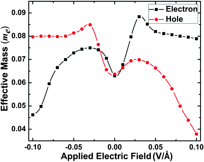
As an example, the evolution of the effective electron and hole mass (in units of the free electron mass me) of the 16bn@CNT under the −0.10 to +0.10 V Å−1 is calculated and presented in Fig. 10. From this calculation, the effective electron and hole mass increase from the ground state to the electric fields of −0.03 and +0.03 V Å−1 and decrease below −0.03 V Å−1 and above +0.03 V Å−1. As a small effective mass reflects a high mobility and conductivity, the Fig. 10 results show that under low (−0.10 V Å−1) and high (+0.10 V Å−1) electric fields, the 16bn@CNT demonstrates a metallic behavior. With an increasing negative (positive) electric field applied, the effective electron (hole) mass decreases obviously, while the effective hole (electron) mass reduces slightly. It illustrates the electron (hole) plays the most important role in electron transport under the negative (positive) gates, and the carrier mobility and electronic structure of 16bn@CNT can be effectively modulated by the applied electric field.
 | ||
| Fig. 10 The evolutions of effective electron and hole mass (in units of the free electron mass me) of 16bn@CNT under different electric field applied along the y axis. | ||
4 Conclusions
Using first-principles density functional theory calculations, we investigated the band gap opening and modulating of a new class of semiconducting armchair SWCNT with a BN line defect. It is found that the BN line defect not only breaks the structural symmetry of the armchair SWCNT, but also induces shorter BN bond with higher bond energy and three permanent dipole moments to enhance the band gap opening, while the dipole moment along the z axis plays the most important role. The calculated results show that the gap opening of bn@CNTs with widths of 4, 8, 12, 16, 20 and 24 are 0.86, 0.60, 0.46, 0.35, 0.27 and 0.24 eV, respectively. The 0.86 eV gap opening of small bn@CNT (i.e. 4bn@CNT) is the largest gap opening ever reported in literature.The band gaps of bn@CNT are modulated using both mechanical and electrical approaches to achieve semiconductor–metal phase transitions. For mechanical modulating, uniaxial compressive strain in the range of 0–3% of the z-axis lattice length are applied for different widths of 4, 8, 12, 16, 20 and 24. It is found the band gaps of most studied bn@CNTs decrease in a linear relationship with increasing compressive strain except the 12bn@CNT and 16bn@CNT, which change slightly during 0–1% strain level. It is also found that applying 3% compressive strain can reduce the band gap of 4bn@CNT from 0.86 eV to 0.49 eV, and 20bn@CNT from 0.27 eV to 0.01 eV. For electrical modulating, the opened band gap is computed between −0.10 to +0.10 V Å−1 electric fields. As found from the study, those large bn@CNTs are more sensitive to the electric field modulating, i.e., for 24bn@CNT, a small voltage of −0.04 (0.04) V Å−1 can reduce their band gaps from 0.24 to 0.02 (0.03) eV; while those small bn@CNTs are slightly resistive to the electric field applied, i.e., the band gaps of 4bn@CNT and 8bn@CNT decrease to 98% (90%) and 90% (70%) under −0.10 (0.10) V Å−1.
Acknowledgements
The work described in this paper was fully supported by grants from the University of Wisconsin Milwaukee Research Growth Initiative grant program and the China National Natural Science Foundation (Grant No. 51302022).References
- S. Iijima and T. Ichihashi, Nature, 1993, 363, 603 CrossRef CAS.
- R. H. Baughman, A. A. Zakhidov and W. A. de Heer, Science, 2002, 297, 787 CrossRef CAS PubMed.
- P. G. Collins, K. Bradley, M. Lshigami and A. Zettl, Science, 2000, 287, 1801 CrossRef CAS PubMed.
- J. Wang, M. Musameh and Y. Lin, J. Am. Chem. Soc., 2003, 125, 2408 CrossRef CAS PubMed.
- K. H. An, W. S. Kim, Y. S. Park, J. M. Moon, D. J. Bae, S. C. Lim, Y. S. Lee and Y. H. Lee, Adv. Funct. Mater., 2001, 11, 387 CrossRef CAS.
- M. Kaempgen, C. K. Chan, J. Ma, Y. Cui and G. Gruner, Nano Lett., 2009, 9, 1872 CrossRef CAS PubMed.
- A. C. Dillon, K. M. Jones, T. A. Bekkedahl, C. H. Kiang, D. S. Bethune and M. J. Heben, Nature, 1997, 386, 377 CrossRef CAS.
- C. Liu, Y. Y. Fan, M. Liu, H. T. Cong, H. M. Cheng and M. S. Dresselhaus, Science, 1999, 286, 1127 CrossRef CAS PubMed.
- S. S. Fan, M. G. Chapline, N. R. Franklin, T. W. Tombler, A. M. Cassell and H. J. Dai, Science, 1999, 283, 512 CrossRef CAS PubMed.
- K. Jensen, J. Weldon, H. Garcia and A. Zettl, Nano Lett., 2007, 7, 3508 CrossRef CAS PubMed.
- Z. Yao, C. L. Kane and C. Dekker, Phys. Rev. Lett., 2000, 84, 2941 CrossRef CAS PubMed.
- J. Nygard, D. H. Cobden and P. E. Lindelof, Nature, 2000, 408, 342 CrossRef CAS PubMed.
- J. W. G. Wilder, L. C. Venema, A. G. Rinzler, R. E. Smalley and C. Dekker, Nature, 1998, 391, 59 CrossRef.
- A. J. Du, Y. Chen, Z. H. Zhu, G. Q. Lu and S. C. Smith, J. Am. Chem. Soc., 2009, 131, 1682 CrossRef CAS PubMed.
- V. V. Deshpande, B. Chandra, R. Caldwell, D. S. Novikov, J. Hone and M. Bockrath, Science, 2009, 323, 106 CrossRef CAS PubMed.
- H. X. Lu, J. B. Wu and W. Y. Zhang, Phys. Rev. B: Condens. Matter Mater. Phys., 2013, 88, 035423 CrossRef.
- D. Connétable, G. M. Rignanese, J. C. Charlier and X. Blase, Phys. Rev. Lett., 2005, 94, 015503 CrossRef PubMed.
- G. Dumont, P. Boulanger, M. Côté and M. Ernzerhof, Phys. Rev. B: Condens. Matter Mater. Phys., 2010, 82, 035419 CrossRef.
- V. H. Crespi, M. L. Cohen and A. Rubio, Phys. Rev. Lett., 1997, 79, 2093 CrossRef CAS.
- V. V. Ivanovskaya, A. Zobelli, O. Stéphan, P. R. Briddon and C. Colliex, J. Phys. Chem. C, 2009, 113, 16603 CAS.
- A. Kleiner and S. Eggert, Phys. Rev. B: Condens. Matter Mater. Phys., 2001, 63, 073408 CrossRef.
- P. Delaney, H. J. Choi, J. Ihm, S. G. Louie and M. L. Cohen, Nature, 1998, 391, 466 CrossRef CAS.
- P. Delaney, H. J. Choi, J. Ihm, S. G. Louie and M. L. Cohen, Phys. Rev. B: Condens. Matter Mater. Phys., 1999, 60, 7899 CrossRef CAS.
- M. Ouyang, J. L. Huang, C. L. Cheung and C. M. Lieber, Science, 2001, 292, 702 CrossRef CAS PubMed.
- C. K. Yang, J. J. Zhao and J. P. Lu, Nano Lett., 2004, 4, 561 CrossRef CAS.
- J. Y. Lee and J. H. Cho, Appl. Phys. Lett., 2006, 89, 023124 CrossRef.
- M. R. Amer, A. Bushmaker and S. B. Cronin, Nano Lett., 2012, 12, 4843 CrossRef CAS PubMed.
- X. Y. Zhao, C. M. Wei, L. Yang and M. Y. Chou, Phys. Rev. Lett., 2004, 92, 236805 CrossRef PubMed.
- Z. G. Wu, J. B. Neaton and J. C. Grossman, Phys. Rev. Lett., 2008, 100, 246804 CrossRef PubMed.
- S. Mandal. and R. Pati, Chem. Phys. Lett., 2009, 479, 244 CrossRef CAS.
- J. A. Brehm, S. M. Young, F. Zheng and A. M. Rappe, J. Appl. Phys., 2013, 114, 224304 CrossRef.
- J. Lee, H. Kim, S. J. Kahng, G. Kim, Y. W. Son, J. Ihm, H. Kato, Z. W. Wang, T. Okazaki, H. Shinohara and Y. Kuk, Nature, 2002, 415, 1005 CrossRef CAS PubMed.
- M. Cha, S. Jung, M. H. Cha, G. Kim, J. Ihm and J. Lee, Nano Lett., 2009, 9, 1345 CrossRef CAS PubMed.
- E. S. Jeng, A. E. Moll, A. C. Roy, J. B. Gastala and M. S. Strano, Nano Lett., 2006, 6, 371 CrossRef CAS PubMed.
- D. A. Heller, E. S. Jeng, T. K. Yeung, B. M. Martinez, A. E. Moll, J. B. Gastala and M. S. Strano, Science, 2006, 311, 508 CrossRef CAS PubMed.
- D. S. Novikov and L. S. Levitov, Phys. Rev. Lett., 2006, 96, 036402 CrossRef CAS PubMed.
- S. J. Tans, A. R. M. Verschueren and C. Dekker, Nature, 1998, 393, 49 CrossRef CAS.
- R. Martel, T. Schmidt, H. R. Shea, T. Hertel and Ph. Avouris, Appl. Phys. Lett., 1998, 73, 2447 CrossRef CAS.
- C. L. Kane and E. J. Mele, Phys. Rev. Lett., 1997, 78, 1932 CrossRef CAS.
- L. Yang and J. Han, Phys. Rev. Lett., 2000, 85, 154 CrossRef CAS PubMed.
- U. C. Coskun, T. C. Wei, S. Vishveshwara, P. M. Goldbart and A. Bezryadin, Science, 2004, 304, 1132 CrossRef CAS PubMed.
- W. Clauss, D. J. Bergeron and A. T. Johnson, Phys. Rev. B: Condens. Matter Mater. Phys., 1998, 58, R4266 CrossRef CAS.
- T. W. Tombler, C. W. Zhou, L. Alexseyev, J. Kong, H. J. Dai, L. Liu, C. S. Jayanthi, M. J. Tang and S. Y. Wu, Nature, 2000, 405, 769 CrossRef CAS PubMed.
- C. Gómez-Navarro, J. J. Sáenz and J. Gómez-Herrero, Phys. Rev. Lett., 2006, 96, 076803 CrossRef PubMed.
- J. Q. Lu, J. Wu, W. H. Duan, F. Liu, B. F. Zhu and B. L. Gu, Phys. Rev. Lett., 2003, 90, 156601 CrossRef PubMed.
- C. J. Park, Y. H. Kim and K. J. Chang, Phys. Rev. B: Condens. Matter Mater. Phys., 1999, 60, 10656 CrossRef CAS.
- Z. Yao, C. L. Kane and C. Dekker, Phys. Rev. Lett., 2000, 84, 2941 CrossRef CAS PubMed.
- J. Klinovaja, S. Gangadharaiah and D. Loss, Phys. Rev. Lett., 2012, 108, 196804 CrossRef PubMed.
- J. O'Keeffe, C. Y. Wei and K. Cho, Appl. Phys. Lett., 2002, 80, 676 CrossRef.
- Y. Li, S. V. Rotkin and U. Ravaioli, Nano Lett., 2003, 3, 183 CrossRef CAS.
- F. Xu, M. Y. Wu, N. S. Safron, S. S. Roy, R. M. Jacobberger, D. J. Bindl, J. H. Seo, T. H. Chan, Z. Q. Ma and M. S. Arnold, Nano Lett., 2014, 14, 682 CrossRef CAS PubMed.
- P. Koskinen, S. Malola and H. Häkkinen, Phys. Rev. B: Condens. Matter Mater. Phys., 2009, 80, 073401 CrossRef.
- A. Cresti and S. Roche, Phys. Rev. B: Condens. Matter Mater. Phys., 2009, 79, 233404 CrossRef.
- Z. Liu, K. Suenaga, P. J. F. Harris and S. Iijima, Phys. Rev. Lett., 2009, 102, 015501 CrossRef PubMed.
- K. Suenaga and M. Koshino, Nature, 2010, 468, 1088 CrossRef CAS PubMed.
- J. S. Kim, J. H. Warner, A. W. Robertson and A. I. Kirkland, ACS Nano, 2015, 9, 8916 CrossRef CAS PubMed.
- K. He, A. W. Robertson, S. Lee, E. Yoon, G. D. Lee and J. H. Warner, Nano Lett., 2014, 8, 12272 CAS.
- O. Hod, V. Barone, J. E. Peralta and G. E. Scuseria, Nano Lett., 2007, 7, 2295 CrossRef CAS PubMed.
- E. J. Kan, Z. Y. Li, J. L. Yang and J. G. Hou, J. Am. Chem. Soc., 2008, 130, 4224 CrossRef CAS PubMed.
- M. H. Wu, Y. Pei and X. C. Zeng, J. Am. Chem. Soc., 2010, 132, 5554 CrossRef CAS PubMed.
- D. V. Kosynkin, A. L. Higginbotham, A. Sinitskii, J. R. Lomeda, A. Dimiev, B. K. Price and J. M. Tour, Nature, 2009, 458, 872 CrossRef CAS PubMed.
- V. Barone, O. Hod and G. E. Scuseria, Nano Lett., 2006, 6, 2748 CrossRef CAS PubMed.
- D. Gunlycke, J. W. Li, J. W. Mintmire and C. T. White, Nano Lett., 2010, 10, 3638 CrossRef CAS PubMed.
- J. Li, Z. H. Zhang, D. Wang, Z. Zhu, Z. Q. Fan, G. P. Tang and X. Q. Deng, Carbon, 2014, 69, 142 CrossRef CAS.
- Ž. Šljivančanin, Phys. Rev. B: Condens. Matter Mater. Phys., 2011, 84, 085421 CrossRef.
- K. W. Lee and C. E. Lee, Adv. Mater., 2012, 24, 2019 CrossRef CAS PubMed.
- Y.-W. Son, M. L. Cohen and S. G. Louie, Nature, 2006, 444, 347 CrossRef CAS PubMed.
- M. Brandbyge, J.-L. Mozos, P. Ordejón, J. Taylor and K. Stokbro, Phys. Rev. B: Condens. Matter Mater. Phys., 2002, 65, 165401 CrossRef.
- J. M. Soler, E. Artacho, J. D. Gale, A. García, J. Junquera, P. Ordejón and D. Sánchez-Portal, J. Phys.: Condens. Matter, 2002, 14, 2745 CrossRef CAS.
- P. Ayala, R. Arenal, A. Loiseau, A. Rubio and T. Pichler, Rev. Mod. Phys., 2010, 82, 1843 CrossRef CAS.
- L. J. Ci, L. Song, C. H. Jin, D. Jariwala, D. X. Wu, Y. J. Li, A. Srivastava, Z. F. Wang, K. Storr, L. Balicas, F. Liu and P. M. Ajayan, Nat. Mater., 2010, 9, 430 CrossRef CAS PubMed.
- L. Song, L. Balicas, D. J. Mowbray, R. B. Capaz, K. Storr, L. J. Ci, D. Jariwala, S. Kurth, S. G. Louie, A. Rubio and P. M. Ajayan, Phys. Rev. B: Condens. Matter Mater. Phys., 2012, 86, 075429 CrossRef.
- J. P. Perdew, K. Burke and M. Ernzerhof, Phys. Rev. Lett., 1996, 77, 3865 CrossRef CAS PubMed.
- D. R. Kauffman, D. C. Sorescu, D. P. Schofield, B. L. Allen, K. D. Jordan and A. Star, Nano Lett., 2010, 10, 958 CrossRef CAS PubMed.
- Q. M. Yan, B. Huang, J. Yu, F. W. Zheng, J. Zang, J. Wu, B. L. Gu, F. Liu and W. H. Duan, Nano Lett., 2007, 7, 1469 CrossRef CAS PubMed.
- J. C. Dong and H. Li, J. Phys. Chem. C, 2012, 116, 17259 CAS.
- E. Lyyamperumal, S. Y. Wang and L. M. Dai, ACS Nano, 2012, 6, 5259 CrossRef PubMed.
- L. Pauling, J. Am. Chem. Soc., 1932, 54, 3570 CrossRef CAS.
- D. Gunlycke, J. W. Li, J. W. Mintmire and C. T. White, Nano Lett., 2010, 10, 3638 CrossRef CAS PubMed.
- F. W. Averill, J. R. Morris and V. R. Cooper, Phys. Rev. B: Condens. Matter Mater. Phys., 2009, 80, 195411 CrossRef.
- X. J. Zhou, J. Y. Park, S. M. Huang, J. Liu and P. L. McEuen, Phys. Rev. Lett., 2005, 95, 146805 CrossRef PubMed.
Footnote |
| † Electronic supplementary information (ESI) available. See DOI: 10.1039/c5cp06853c |
| This journal is © the Owner Societies 2016 |