
 Open Access Article
 This Open Access Article is licensed under a
 Creative Commons Attribution 3.0 Unported Licence
Nitrogenated, phosphorated and arsenicated monolayer holey graphenes
Mehmet
Yagmurcukardes
*a,
Seyda
Horzum
bc,
Engin
Torun
b,
Francois M.
Peeters
b and
R.
Tugrul Senger
*a
aDepartment of Physics, Izmir Institute of Technology, 35430 Izmir, Turkey. E-mail: mehmetyagmurcukardes@iyte.edu.tr; tugrulsenger@iyte.edu.tr
bDepartment of Physics, University of Antwerp, Groenenborgerlaan 171, 2020 Antwerp, Belgium
cDepartment of Engineering Physics, Faculty of Engineering, Ankara University, 06100 Ankara, Turkey
First published on 22nd December 2015
Abstract
Motivated by a recent experiment that reported the synthesis of a new 2D material nitrogenated holey graphene (C2N) [Mahmood et al., Nat. Commun., 2015, 6, 6486], the electronic, magnetic, and mechanical properties of nitrogenated (C2N), phosphorated (C2P) and arsenicated (C2As) monolayer holey graphene structures are investigated using first-principles calculations. Our total energy calculations indicate that, similar to the C2N monolayer, the formation of the other two holey structures are also energetically feasible. Calculated cohesive energies for each monolayer show a decreasing trend going from the C2N to C2As structure. Remarkably, all the holey monolayers considered are direct band gap semiconductors. Regarding the mechanical properties (in-plane stiffness and Poisson ratio), we find that C2N has the highest in-plane stiffness and the largest Poisson ratio among the three monolayers. In addition, our calculations reveal that for the C2N, C2P and C2As monolayers, creation of N and P defects changes the semiconducting behavior to a metallic ground state while the inclusion of double H impurities in all holey structures results in magnetic ground states. As an alternative to the experimentally synthesized C2N, C2P and C2As are mechanically stable and flexible semiconductors which are important for potential applications in optoelectronics.
1 Introduction
In the last decade, graphene, one atom thick form of carbon atoms arranged in a honeycomb structure, has become important in materials science due to its exceptional properties.1,2 It has triggered interest in novel two dimensional structures such as hexagonal monolayer crystals of III–V binary compounds3,4 and transition metal dichalcogenides (TMDs).3,5,6 Hexagonal monolayer structures of BN7,8 and AlN9–13 are wide band gap semiconductors with nonmagnetic ground states. However, monolayer crystals of TMDs such as MoS2, WS2, MoSe2, WSe2, MoTe2 have direct band gaps in a favorable range of 1–2 eV, and they are potentially important for optoelectronic device technology.The lack of a band gap is the major obstacle for the use of graphene in electronic applications such as field-effect transistors,14 and electrodes in solar cells.15,16 Thus, tuning its electrical properties through opening of a band gap is of great technological importance.14,17,18 Nitrogen doping has been widely studied as one of the most feasible methods to modulate the electronic and other properties of graphene and its derivatives.19–24
A series of covalent organic frame-works (COFs)25–29 have been designed to form large graphene-like honeycomb networks. In 2005, Yaghi et al. demonstrated the utility of the topological design principle in the synthesis of porous organic frameworks which are connected with covalent bonds, which are the first successful examples of these COFs.30 Since COFs are composed of light-weight elements linked by strong covalent bonds, they have low mass densities and possess high thermal stability. The successful realization of COFs with molecular graphene-type building blocks would provide covalent frameworks that could be functionalized into light-weight materials optimized for gas storage, photonic, and catalytic applications.31,32
N-Doped graphene-like honeycomb structures are important examples of COF materials. In a recent study by Mahmood et al.33 the design and preparation of a two dimensional holey crystal, C2N, with uniform holes and nitrogen atoms was reported. The structure and band gap of C2N were studied by using both experimental techniques and DFT-based calculations. This new structure is layered like graphite with a different interlayer distance and is highly crystalline. It exhibits a direct band gap which was determined to be 1.96 eV by using ultraviolet visible spectroscopy, while a slightly smaller band gap of 1.70 eV is obtained from density functional theory (DFT) calculations. In another study, Sahin investigated the structural and phononic characteristics of the C2N structure.34 The formation of heterostructures of holey graphenes and the resulting Moiré patterns were investigated by Kang et al.35 Very recently Zhang et al. investigated the structural and electronic properties of few-layer C2N by considering different stacking orders and number of layers.36 In the study by Xu et al. energy barriers for the adsorption of H2, CO2 and CO molecules on the C2N monolayer were calculated for a possible H2 dissociation.37
Motivated by the recent experiment on the synthesis of the C2N monolayer33 and by the studies on graphene-like networks composed of COFs, we investigate the structural, electronic and mechanical properties of 2D holey crystals of C2X (X = N, P or As) stoichiometry. The mechanical properties of these hexagonal structures are examined under uniaxial strain, and the in-plane stiffness and the Poisson ratio values are obtained. In addition, the most probable types of atomic scale disorder, the formation of N, P and As defects, are investigated for these holey structures.
The paper is organized as follows: details of the computational methodology are given in Section 2. Structural properties of C2N, C2P and C2As are presented in Section 3. Discussions about electronic and magnetic properties of these monolayer crystals are given in Section 4. In Section 5 the mechanical properties are discussed by examining the in-plane stiffness and the Poisson ratio for each structure. Electronic and geometric properties of defect and H-impurities in C2X monolayers are discussed in Section 6. Finally we conclude in Section 7.
2 Computational methodology
First-principles calculations were performed within the framework of density functional theory (DFT) by using the Vienna Ab initio Simulation Package (VASP).40–43 The approach is based on an iterative solution of the Kohn–Sham equations44 with a plane-wave set adopted with the Perdew–Burke–Ernzerhof (PBE) exchange–correlation functional of the generalized gradient approximation (GGA)45,46 with the inclusion of spin-orbit-coupling (SOC). More accurate results and electronic structure calculations were performed using the Heyd–Scuseria–Ernzerhof (HSE) screened-nonlocal-exchange functional of the generalized Kohn–Sham scheme.47 Analysis of the charge transfers in the structures was made by the Bader technique.48Electronic and geometric relaxations of hexagonal monolayers of C2X structures were performed by considering the following criteria in our calculations. The energy cut-off value for the plane wave basis set was taken to be 500 eV. The energy difference between sequential steps for the electronic self consistence-loop was considered to be 10−5 eV. As a convergence criterion in the structural relaxation and for the Hellmann–Feynman forces on each atom was taken to be 0.05 eV Å−. For geometric relaxation of the structures a parallelogram unit cell containing 12 C atoms and 6 X atoms was used (see Fig. 1). The minimum energy was obtained by varying the lattice constant and the pressure was reduced below 1 kbar. Brillouin zone integration was performed by using a set of 5 × 5 × 1 Γ-centered k-point sampling mesh for a single unit cell. To get more accurate results for the density of states (DOS) and the work function calculations a set of 15 × 15 × 1 k-point sampling was used. The broadening for DOS calculations was taken to be 0.05. The cohesive energy per atom in a primitive unit cell was calculated using the formula;
| Ecoh = [12EC + 6EX − EC2X]/18 | (1) |
 | ||
| Fig. 1 Top view of the C2X holey graphene monolayer structure where X represents N, P or As atoms. | ||
3 Structural properties
Generic forms of the monolayer structures, C2N, C2P and C2As, display honeycomb symmetry as shown in Fig. 1. All calculated parameters for their relaxed geometries are listed in Table 1. In the primitive unit cell there are 12 C atoms and 6 X atoms, X being N, P or As. The C2N crystal has a planar two dimensional structure with a lattice constant of 8.33 Å which is consistent with the value reported by Mahmood et al.33 The calculated C–C bond length is 1.47 Å while the C–N bonds are 1.34 Å with the C–N–C bond angle being 118 degrees. This bond angle is the largest one of all three structures. This means that the hole between the benzene rings is nearly a perfect hexagon in C2N. Bader charge analysis shows that an average 0.6 e of charge depletion per atom occurs from C atoms to the neighboring N atoms. The cohesive energy per atom is highest for the C2N structure with a value of 7.64 eV, as calculated using eqn (1).| a (Å) | d C–X (Å) | d C–C (Å) | θ CXC (deg) | Magnetic State | Δρ (e) | E coh (eV) | E GGAg (eV) | E HSEg (eV) | Φ (eV) | ν | C (eV Å−2) | |
|---|---|---|---|---|---|---|---|---|---|---|---|---|
| C2N | 8.33 | 1.34 | 1.47 | 118 | NM | −0.6 | 7.64 | 1.66(d) | 2.47(d) | 5.23 | 0.26 | 9.27 |
| C2P | 9.33 | 1.76 | 1.42 | 108 | NM | +0.6 | 6.84 | 0.22(i) | 0.94(d) | 4.90 | 0.21 | 6.69 |
| C2As | 9.72 | 1.92 | 1.41 | 108 | AFM | +0.3 | 5.78 | 0.43(d) | 1.16(d) | 4.89 | 0.21 | 5.83 |
| Graphene | 2.46 | — | 1.42 | 120 | NM | 0.0 | 7.97 | — | — | 4.51 | 0.1638 | 21.2538 |
| h-BN | 2.51 | 1.45 (B–N) | — | 120 | NM | +2.1 | 7.10 | 4.48(d) | 5.56(d)39 | 5.80 | 0.22 | 17.12 |
Optimized lattice constant of the C2P monolayer crystal is calculated to be 9.33 Å. The C–C bond length is 1.42 Å as in graphene hexagons and the C–P bond length is 1.76 Å. The C–P–C bonds have a narrower angle than that of the C–N–C bonds with a value of 108 degrees. According to the Bader charge analysis, opposite to the C2N case an average of 0.6 e charge is transferred to each C atom from the P atoms. The cohesive energy per atom, 6.84 eV is less than that of C2N.
For the C2As monolayer structure the lattice constant is 9.72 Å with a corresponding C–C bond length of 1.41 Å which is nearly the same as the C–C bond in C2P. The longest bond length between a C atom and its X neighbor is found for the C–As bond with a value of 1.92 Å. The angle between two C–As bonds, 108 degrees, is smaller than that of the C–N bonds. We found that the charge transfer occurs in this structure from As atoms to each C atom with a value of 0.3 e. The charge transfer occurs from P and As atoms to the C rings for C2P and C2As, respectively. However, it occurs from C rings to the N atoms in C2N.
4 Electronic and magnetic properties
The calculated lattice constant and electronic band gap of C2N are in agreement with the values reported by Mahmood et al.33 The C2N monolayer has a direct band gap of 1.66 eV and 2.47 eV in GGA and HSE06 levels, respectively, as seen in Fig. 2(a). The overall dispersion characteristics of the bands are not affected by the inclusion of HSE06. The valence band maximum (VBM) and the conduction band minimum (CBM) of the C2N monolayer lie at the Γ point of the Brillouin zone. Relatively large value of the C2N energy band gap makes it a suitable semiconductor for various device applications. It also appears from the energy band structure that spin up and spin down states are degenerate throughout the Brillouin zone and therefore the structure does not exhibit any spin polarization in its ground state. Due to the pairing of pz electrons of 3-coordinated C atoms and 2-coordinated N atoms, the structure has a nonmagnetic ground state.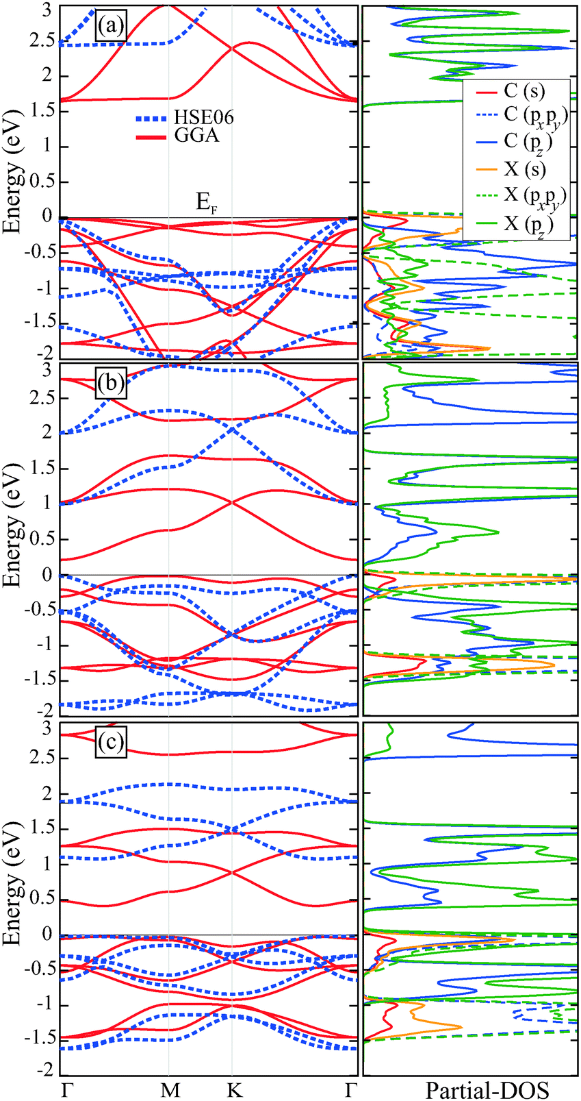 | ||
| Fig. 2 Band-structures (left-panel) and corresponding partial density of states (right-panel) of (a) C2N, (b) C2P, and (c) C2As where red curves are for bands calculated within GGA approximation while dashed blue curves are for bands calculated within HSE06 on top of GGA. The Fermi energy (EF) level is set to the valence band maximum. | ||
The electronic band dispersion for the C2P monolayer crystal indicates that it has an indirect band gap of 0.22 eV and a direct gap of 0.94 eV in GGA and HSE06 calculations, respectively. Since the VBM of the C2P monolayer consists of localized states, these states are affected by the HSE06 functional and the VBM point of the band structure moves to the Γ point as shown in Fig. 2(b). Like the C2N monolayer, C2P has also a nonmagnetic ground state.
In Table 1, the workfunctions of the monolayer holey graphenes are also shown. It is seen that the workfunction values of these compounds are smaller than that of the h-BN and larger than the value for graphene. Comparing the workfunction values of the monolayers a decreasing trend can be seen from nitrogenated one to the arsenicated one. This result can be explained by the decreasing ionization energy of the elements in the periodic table from top to bottom rows.
The C2As monolayer crystal is a semiconductor with a direct band gap of 0.43 eV and 1.16 eV in GGA and HSE06 levels, respectively. Similar to the case of C2N, the inclusion of the HSE06 functional increases the energy gap and does not change the dispersion characteristic of the band structure (see Fig. 2(c)). Both the VBM and the CBM of C2As lie between the Γ and the M points. Interestingly, there is an isolated Dirac point in the conduction band of C2As which can be populated using doping or a gate potential. The net magnetic moment for this structure is zero like for the other two monolayers. But the ground state is obtained for anti-ferromagnetic (AFM-1) ordering given in Fig. 3(a) in which all the neighboring C and As atoms have equal but opposite local magnetic moments in their sublattices. In the AFM-2 magnetic ordering, the C atoms in a ring have opposite magnetic moments while the As atoms have ferromagnetically ordered moments as seen in Fig. 3(b). The net magnetic moments of the two configurations, AFM-1 and AFM-2, are zero with an energy difference of 50 meV, AFM-1 being the ground state.
 | ||
| Fig. 3 Charge density difference, ρup − ρdown, of the C2As monolayer structure for (a) fully anti-ferromagnetic (AFM-1) order and (b) anti-ferromagnetic order in the benzene ring (AFM-2) where green/yellow color is for minority/majority spin states. The plotted isosurface values are 10−3e Å−3 and 10−5e Å−3 for (a) and (b) respectively. | ||
5 Mechanical properties
The elastic properties of homogeneous and isotropic materials can be represented by two independent constants, the in-plane stiffness C and the Poisson ratio ν. The stiffness parameter is a measure of the rigidity or the flexibility of a material. The mechanical response of a material to an applied stress is called the Poisson ratio. It is also defined as the ratio of the transverse contraction strain to the longitudinal extension strain in the direction of the stretching force, that is ν = −εtrans/εaxial.To calculate the elastic constants of C2N, C2P and C2As monolayers, a 2 × 2 supercell containing 72 atoms is considered. The strains εx and εy are applied to the monolayer crystals by varying the lattice constants along the x and y directions. The strain parameters εx and εy are varied between ±0.02 with a step size of 0.01. For this purpose three different sets of data are calculated; (i) εy = 0 and εx varying, (ii) εx = 0 and εy varying and (iii) εx = εy. At each configuration, the atomic positions are fully relaxed and the strain energy, ES, is calculated by subtracting the total energy of the strained system from the equilibrium total energy. The calculated data are fitted to the equation ES = c1εx2 + c2εy2 + c3εxεy, so that the coefficients ci are determined. The in-plane stiffness C can then be calculated from C = (1/A0)(2c − c32/2c) where we let c1 = c2 = c due to isotropy of the unit cell and A0 is the unstretched area of the 2 × 2 supercell. The Poisson ratio is obtained as ν = c3/2c. Due to the symmetry of the honeycomb lattice, the in-plane stiffness and the Poisson ratio are the same along the x and y directions.
As indicated in Table 1, the calculated in-plane stiffness for C2N is 9.27 eV Å−2 which has the highest value among the three monolayer structures. This value indicates a strong bonding between the C and N atoms. Although it is the highest value, it is still smaller compared to that of graphene and h-BN.38 The calculated Poisson ratio for the C2N monolayer is 0.26 which is in the range for usual two dimensional materials. This means that when the material is compressed in one direction, it will expand in the other direction as well. The in-plane stiffness value for C2P is calculated (6.69 eV Å−2) with a corresponding Poisson ratio of 0.21, which means that the C2P crystal is less responsive than C2N under compression. The lowest in-plane stiffness for the C2As monolayer is 5.83 eV Å−2 with the corresponding Poisson ratio of 0.21 which is equal to that of the C2P crystal. All the holey monolayers have Poisson ratios which are larger than that of graphene and close to that of h-BN.
We next consider the behavior of the monolayer structures under higher values of uniform strain ranging from 0.04 to 0.40. For this purpose the calculations are performed in a 2 × 2 supercell. The change in strain energy of all the monolayers under applied biaxial strain is given in Fig. 4(a). Although C2N is the stiffest crystal, structural deformations start to form beyond 12% strain which is small compared to those of C2P and C2As. By structural deformation we mean that the N atoms connecting the C pairs start to form C4N2 isolated hexagonal rings. The distance between two neighboring C atoms in different hexagonal rings becomes 1.79 Å at 12% strain. This distance increases up to 3.10 Å at 40% strain. The deformation path seems to be the same for the C2P monolayer structure. Up to a strain value of 20%, P atoms are still bonded to the hexagonal C rings and there is no drastic change in the structure of the monolayer. However beyond 20% strain hexagonal rings are formed composed of 4-C and 2-P atoms as in the case of C2N. The C–C bond lengths in C pairs are approximately 1.30 Å at 20% strain and there exist C–C pairs connected by P atoms as shown in Fig. 4(c). Among the monolayer structures considered, only in the C2As crystal the hexagonal C rings preserve their form under large strains. The bond angle of the C–As–C bond gets larger as the applied strain is increased. As given in Fig. 4(d), at 24% strain this angle becomes 158 degrees and there is no longer bonding between the C and As atoms. Compared with the other two structures, C2As has the smallest in-plane stiffness value and it is the softest material among the three monolayers. The C2X monolayer structures can be viewed as an ordered phase of 6-C rings linked by the X atoms. It seems that the linker atoms N and P have stronger bonds to their C neighbors so that the structure dissociates into isolated rings by breaking the C–C bonds under high strain. For As, however, the C–C bonds must be stronger than the C–As bonds so that the crystal yields at the linker sites.
 | ||
| Fig. 4 (a) Change in total energy of the three holey graphene monolayers under applied strain. Structural changes under applied strain of (b) C2N, (c) C2P and (d) C2As. | ||
6 Effect of defects
Considering the synthesis procedure of the mentioned holey crystals in which the ingradient molecules are self-assembled, the atomic scale disorders like vacant N, P and As sites are the most probable disorders in C2N, C2P and C2As monolayers, respectively. The existence of H-impurities at these vacant-sites are also possible since the C2N holey structure is synthesized as a result of the interactions of hexaaminobenzene and hexaketocyclohexane molecules which contain H atoms in their composition. In this section, we investigate the effects of these vacant sites and substitutional H-impurities on the geometric and electronic properties of the monolayer holey structures.Optimized geometries of the defected structures are shown in Fig. 5. For the N-defected C2N and P-defected C2P holey crystals (Fig. 5(a) and (b)), removal of a single N or P atom results in a bond formation between the two C atoms at the vacant site. However, in the case of As-defected C2As the optimized geometric structure does not lead to an additional bonding (see Fig. 5(c)). Geometry optimizations indicate that for X-vacant structures only the C2N retains its planar geometry while the other two structures get buckled. Our Bader analysis shows that charge depletion of 1.1 e per atom occurs from the C atoms to the neighboring N atoms in N-defected C2N. For P-defected C2P, an average of 0.6 e charge is transferred to each C atom except for the two C atoms at the vacant sites since these C atoms keep approximately their initial charges. For As-defected C2As the charge is depleted to the C atoms with a value of 0.3 e per atom on the average. We found that the N-defected C2N has a nonmagnetic ground state while P-defected C2P and As-defected C2As have magnetic ground states with a net moment of 1 μB. Total DOS calculations indicate that X-missing structures of C2N and C2P become metallic monolayers while the As-defected C2As is still a semiconductor with a lower band gap energy than its perfect form (see Fig. 6(c)). Calculated cohesive energies per atom in the supercells demonstrate that for all three structures the highest Ecoh occur for X-missing structures of C2N and C2P while for the C2As monolayer the most energetic case is 1H-impurity case as seen in Table 2.
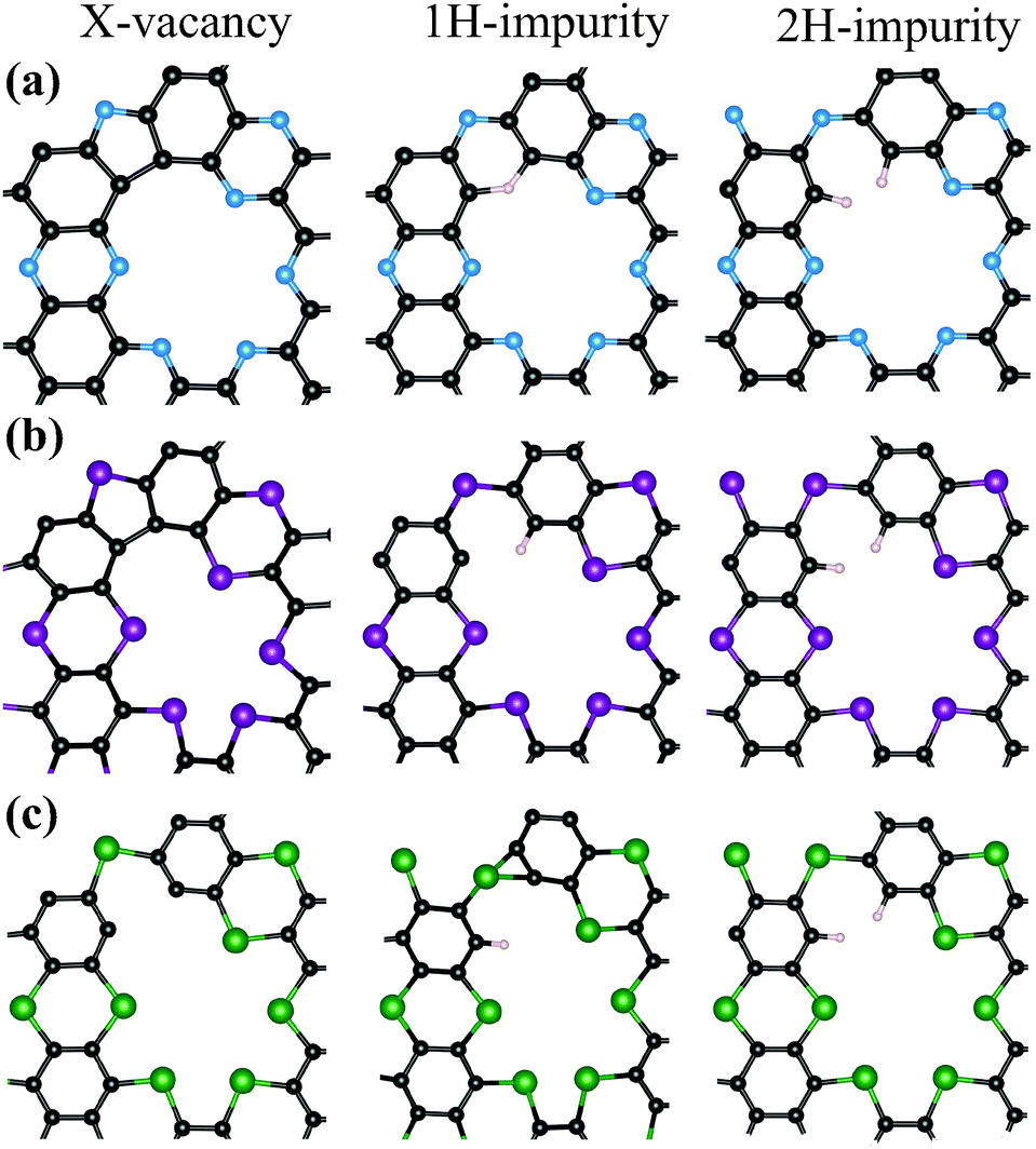 | ||
| Fig. 5 Optimized X-vacancy and their H substituted structures of (a) C2N, (b) C2P, and (c) C2 As respectively. | ||
 | ||
| Fig. 6 Total DOS for defected and H-impurity structures of (a) C2N, (b) C2P, and (c) C2As respectively. | ||
| Geometry | a (Å) | b (Å) | μ (μB) | E coh (eV) | |
|---|---|---|---|---|---|
| N-Vacant-C2N | Planar | 16.44 | 16.44 | 0 | 6.77 |
| P-Vacant-C2P | Buckled | 17.66 | 17.67 | 1 | 6.02 |
| As-Vacant-C2As | Buckled | 19.27 | 19.27 | 1 | 5.61 |
| 1H-imp.-C2N | Planar | 16.63 | 16.63 | 0 | 6.71 |
| 1H-imp.-C2P | Buckled | 18.37 | 18.15 | 0 | 5.97 |
| 1H-imp.-C2As | Buckled | 18.37 | 19.04 | 0 | 5.65 |
| 2H-imp.-C2N | Planar | 16.79 | 16.79 | 1 | 6.67 |
| 2H-imp.-C2P | Planar | 18.71 | 18.71 | 1 | 5.93 |
| 2H-imp.-C2As | Planar | 19.46 | 19.45 | 1 | 5.58 |
As seen in Fig. 5(a), the C2N structure having a single H substitution at the N-vacant site preserves the geometry of the C2N monolayer. The geometries of other two monolayers with 1H-impurity get buckled as seen in Fig. 5. The results of the Bader analysis for all three monolayers for the 1H-impurity case show that 0.1 e of charge is transferred to the C atom at the vacant site from H atoms. The inclusion of single H-impurity gives rise to a non-magnetic ground state for all C2X monolayers as in their bare cases. For 1H-impurity structures the total DOS calculations indicate that all three monolayers preserve their semiconducting character but with lower values of band gap energies (see Fig. 6).
In our study, inclusion of 2H-impurities at the X-vacant sites is also considered. In all three defected structures each H atom binds to a single C atom as expected (see Fig. 5). Addition of the second H atom to the vacancy sites restores the planar geometry of all three monolayers. In this case, the charge is donated to each C atom at the vacant site from the H atoms such that the final charges on C atoms are the same as their values in the perfect crystals. 2H impurities result in a magnetic ground state for all three monolayers with a 1 μB of net magnetic moment. The total DOS calculations demonstrate that inclusion of 2H-impurities in C2X structures preserves the semiconducting behaviors of the three monolayers with lower band gap energies (see Fig. 6). The corresponding cohesive energies per atom are also given in Table 2 which indicate that the C2N monolayer has the highest Ecoh than that of C2P and C2As monolayers.
7 Conclusions
Motivated by recent experiments on the C2N monolayer and graphene-like COF networks, we investigated structural, mechanical and electronic properties of two other monolayer structures, C2P and C2As. We found that C2N has the highest Ecoh among the three monolayers and the calculated values of Ecoh are comparable with that of graphene and h-BN. Moreover, it is calculated that the workfunction values of the monolayers are decreasing from C2N to C2As which is consistent with the trend in ionization energy of each element. Energy-band structure calculations show that all three monolayers are direct band gap semiconductors. Our calculations on mechanical constants suggest that the stiffest material is the C2N structure with the highest Poisson ratio among the three monolayers. Moreover, the vacancy defects of N and P atoms in holey structures lead to metallic ground states while the substitutional H-impurities do not change their semiconducting character but can create net magnetization on the monolayer. Finally, we point out that holey graphene monolayers are new two dimensional materials that are mechanically stable and they are flexible semiconductors which may be favorable for applications in optoelectronics.Acknowledgements
This work was supported by the Flemish Science Foundation (FWO-Vl) and the Methusalem foundation of the Flemish government. Computational resources were provided by TUBITAK ULAKBIM, High Performance and Grid Computing Center (TR-Grid e-Infrastructure).References
- K. S. Novoselov, A. K. Geim, S. Morozov, D. Jiang, Y. Zhang, S. Dubonos, I. Grigorieva and A. Firsov, Science, 2004, 306, 666–669 CrossRef CAS PubMed.
- K. Novoselov, A. K. Geim, S. Morozov, D. Jiang, M. Katsnelson, I. Grigorieva, S. Dubonos and A. Firsov, Nature, 2005, 438, 197–200 CrossRef CAS PubMed.
- K. Novoselov, D. Jiang, F. Schedin, T. Booth, V. Khotkevich, S. Morozov and A. Geim, Proc. Natl. Acad. Sci. U. S. A., 2005, 102, 10451–10453 CrossRef CAS PubMed.
- H. Sahin, S. Cahangirov, M. Topsakal, E. Bekaroglu, E. Akturk, R. T. Senger and S. Ciraci, Phys. Rev. B, 2009, 80, 155453 CrossRef.
- R. Gordon, D. Yang, E. Crozier, D. Jiang and R. Frindt, Phys. Rev. B, 2002, 65, 125407 CrossRef.
- Q. H. Wang, K. Kalantar-Zadeh, A. Kis, J. N. Coleman and M. S. Strano, Nat. Nanotechnol., 2012, 7, 699–712 CrossRef CAS PubMed.
- H. Zeng, C. Zhi, Z. Zhang, X. Wei, X. Wang, W. Guo, Y. Bando and D. Golberg, Nano Lett., 2010, 10, 5049–5055 CrossRef CAS PubMed.
- L. Song, L. Ci, H. Lu, P. B. Sorokin, C. Jin, J. Ni, A. G. Kvashnin, D. G. Kvashnin, J. Lou, B. I. Yakobson and P. M. Ajayan, Nano Lett., 2010, 10, 3209–3215 CrossRef CAS PubMed.
- C. Bacaksiz, H. Sahin, H. D. Ozaydin, S. Horzum, R. T. Senger and F. M. Peeters, Phys. Rev. B, 2015, 91, 085430 CrossRef.
- H. L. Zhuang and R. G. Hennig, Appl. Phys. Lett., 2012, 101, 153109 CrossRef.
- Q. Wang, Q. Sun, P. Jena and Y. Kawazoe, ACS Nano, 2009, 3, 621–626 CrossRef CAS PubMed.
- K. K. Kim, A. Hsu, X. Jia, S. M. Kim, Y. Shi, M. Hofmann, D. Nezich, J. F. Rodriguez-Nieva, M. Dresselhaus, T. Palacios and J. Kong, Nano Lett., 2012, 12, 161–166 CrossRef PubMed.
- M. Farahani, T. S. Ahmadi and A. Seif, THEOCHEM, 2009, 913, 126–130 CrossRef CAS.
- X. Wang, X. Li, L. Zhang, Y. Yoon, P. K. Weber, H. Wang, J. Guo and H. Dai, Science, 2009, 324, 768–771 CrossRef CAS PubMed.
- Y. Xue, J. Liu, H. Chen, R. Wang, D. Li, J. Qu and L. Dai, Angew. Chem., Int. Ed., 2012, 51, 12124–12127 CrossRef CAS PubMed.
- S. Osella, A. Narita, M. G. Schwab, Y. Hernandez, X. Feng, K. Mllen and D. Beljonne, ACS Nano, 2012, 6, 5539–5548 CrossRef CAS PubMed.
- C. Berger, Z. Song, X. Li, X. Wu, N. Brown, C. Naud, D. Mayou, T. Li, J. Hass, A. N. Marchenkov, E. H. Conrad, P. N. First and W. A. de Heer, Science, 2006, 312, 1191–1196 CrossRef CAS PubMed.
- D. Wei, Y. Liu, Y. Wang, H. Zhang, L. Huang and G. Yu, Nano Lett., 2009, 9, 1752–1758 CrossRef CAS PubMed.
- L. Dai, D. W. Chang, J.-B. Baek and W. Lu, Small, 2012, 8, 1130–1166 CrossRef CAS PubMed.
- J. Zhang, F. Zhao, Z. Zhang, N. Chen and L. Qu, Nanoscale, 2013, 5, 3112–3126 RSC.
- L. Dai, Acc. Chem. Res., 2012, 46, 31–42 CrossRef PubMed.
- D. Yu and L. Dai, J. Phys. Chem. Lett., 2010, 1, 467–470 CrossRef CAS.
- K. Gong, F. Du, Z. Xia, M. Durstock and L. Dai, Science, 2009, 323, 760–764 CrossRef CAS PubMed.
- L. Zhao, R. He, K. T. Rim, T. Schiros, K. S. Kim, H. Zhou, C. Gutiérrez, S. Chockalingam, C. J. Arguello and L. Pálová, et al. , Science, 2011, 333, 999–1003 CrossRef CAS PubMed.
- Z. Xiang and D. Cao, J. Mater. Chem. A, 2013, 1, 2691–2718 CAS.
- F. Schltter, F. Rossel, M. Kivala, V. Enkelmann, J.-P. Gisselbrecht, P. Ruffieux, R. Fasel and K. Mllen, J. Am. Chem. Soc., 2013, 135, 4550–4557 CrossRef PubMed.
- J. W. Colson and W. R. Dichtel, Nat. Chem., 2013, 5, 453–465 CrossRef CAS PubMed.
- J. W. Colson, A. R. Woll, A. Mukherjee, M. P. Levendorf, E. L. Spitler, V. B. Shields, M. G. Spencer, J. Park and W. R. Dichtel, Science, 2011, 332, 228–231 CrossRef CAS PubMed.
- X. Feng, X. Ding and D. Jiang, Chem. Soc. Rev., 2012, 41, 6010–6022 RSC.
- A. P. Ct, A. I. Benin, N. W. Ockwig, M. O'Keeffe, A. J. Matzger and O. M. Yaghi, Science, 2005, 310, 1166–1170 CrossRef PubMed.
- H. M. El-Kaderi, J. R. Hunt, J. L. Mendoza-Corts, A. P. Ct, R. E. Taylor, M. O'Keeffe and O. M. Yaghi, Science, 2007, 316, 268–272 CrossRef CAS PubMed.
- S. S. Han, H. Furukawa, O. M. Yaghi, I. William and A. Goddard, J. Am. Chem. Soc., 2008, 130, 11580–11581 CrossRef CAS PubMed.
- J. Mahmood, E. K. Lee, M. Jung, D. Shin, I.-Y. Jeon, S.-M. Jung, H.-J. Choi, J.-M. Seo, S.-Y. Bae and S.-D. Sohn, et al. , Nat. Commun., 2015, 6, 6486 CrossRef CAS PubMed.
- H. Sahin, Phys. Rev. B, 2015, 92, 085421 CrossRef.
- S. H. Jun Kang and F. M. Peeters, Phys. Rev. B, 2015, 92, 195419 CrossRef.
- R. Zhang, B. Li and J. Yang, Nanoscale, 2015, 7, 14062–14070 RSC.
- B. Xu, H. Xiang, Q. Wei, J. Liu, Y. Xia, J. Yin and Z. Liu, Phys. Chem. Chem. Phys., 2015, 17, 15115–15118 RSC.
- C. Lee, X. Wei, J. W. Kysar and J. Hone, Science, 2008, 321, 385–388 CrossRef CAS PubMed.
- N. Berseneva, A. Gulans, A. V. Krasheninnikov and R. M. Nieminen, Phys. Rev. B: Condens. Matter Mater. Phys., 2013, 87, 035404 CrossRef.
- G. Kresse and J. Hafner, Phys. Rev. B, 1993, 47, 558–561 CrossRef CAS.
- G. Kresse and J. Hafner, Phys. Rev. B, 1994, 49, 14251–14269 CrossRef CAS.
- G. Kresse and J. Furthmüller, Comput. Mater. Sci., 1996, 6, 15–50 CrossRef CAS.
- G. Kresse and J. Furthmüller, Phys. Rev. B, 1996, 54, 11169–11186 CrossRef CAS.
- W. Kohn and L. J. Sham, Phys. Rev., 1965, 140, A1133–A1138 CrossRef.
- J. P. Perdew, K. Burke and M. Ernzerhof, Phys. Rev. Lett., 1996, 77, 3865–3868 CrossRef CAS PubMed.
- J. P. Perdew, K. Burke and M. Ernzerhof, Phys. Rev. Lett., 1997, 78, 1396 CrossRef CAS.
- J. Heyd, G. E. Scuseria and M. Ernzerhof, J. Chem. Phys., 2003, 118, 8207–8215 CrossRef CAS.
- G. Henkelman, A. Arnaldsson and H. Jónsson, Comput. Mater. Sci., 2006, 36, 354–360 CrossRef.
| This journal is © the Owner Societies 2016 |