
Photoelectrochemical evidence of nitrogen incorporation during anodizing sputtering – deposited Al–Ta alloys†
A.
Zaffora
a,
M.
Santamaria
*a,
F.
Di Franco
a,
H.
Habazaki
b and
F.
Di Quarto
a
aElectrochemical Materials Science Laboratory, DICAM, Università di Palermo, Viale delle Scienze, Ed. 6, Palermo, Italy. E-mail: monica.santamaria@unipa.it
bGraduate School of Chemical Sciences and Engineering, Hokkaido University, Sapporo, Hokkaido, Japan
First published on 30th November 2015
Abstract
Anodic films were grown to 20 V on sputtering-deposited Al–Ta alloys in ammonium biborate and borate buffer solutions. According to glow discharge optical emission spectroscopy, anodizing in ammonium containing solution leads to the formation of N containing anodic layers. Impedance measurements did not evidence significant differences between the dielectric properties of the anodic films as a function of the anodizing electrolyte. Photoelectrochemical investigation allowed evidencing that N incorporation induces a red-shift in the light absorption threshold of the films due to the formation of allowed localized states inside their mobility gap. The estimated Fowler threshold for the internal photoemission processes of electrons resulted to be independent of the anodizing electrolyte confirming that N incorporation does not appreciably affect the density of states distribution close to the conduction band mobility edge. The transport of photogenerated carriers has been rationalized according to the Pai–Enck model of geminate recombination.
Introduction
The anodizing of aluminium and tantalum has been extensively studied due to the widespread use of the corresponding oxides as dielectric materials in electrolytic capacitors.1,2 In the last decade, it has been proved that anodizing sputtering-deposited aluminium–tantalum alloys is a viable tool to grow Al–Ta mixed oxides, whose composition is a function of the Al/Ta ratio in the base alloy. In ref. 3–5 the structure, composition and physico-chemical properties of such mixed oxides have been widely investigated. Transmission electron micrographs of ultramicrotomed sections revealed that anodic oxides on Al–Ta alloys are amorphous and uniform in thickness, with flat metal/oxide and oxide/electrolyte interfaces. They show nanometric roughness as also confirmed by atomic force microscopy.5 The compositional depth profiles provided by Rutherford back scattering revealed the formation of oxides with uniform composition.3,4 The oxide growth occurred due to simultaneous migrations of cations (Al3+ and Ta5+) outwards and anions (O2−) inwards proceeding in a cooperative manner, developing film materials both at the film/electrolyte and metal/film interfaces, respectively. However, the film structure and the composition are also dependent upon the electrolyte due to the possible incorporation of foreign species from the anodizing bath.6–8 This is very important if we consider that the presence of foreign species in anodic films could affect the electronic properties of the films with possible detrimental effects on the dielectric properties of the oxides.In ref. 9–11 it was shown that during anodizing in ammonium containing solutions of valve metals such as Nb, Ta and Ti, N incorporation occurs with significant effects on the solid state properties of the corresponding oxides. More interestingly, in the case of tantalum, such incorporation is reported to occur only when the electrolyte pH was higher than the pH of zero charge (pHpzc) of Ta2O5, since the negatively charged oxide surface allowed ammonium cations reaching the film and being de-protonated by the imposed electric field.
In this work we want to study if N incorporation occurs during anodizing Al–Ta alloys of different compositions in an ammonium biborate solution. Glow discharge optical emission spectroscopy is used to directly assess the presence of N in the anodic films, while the possible effects on the solid state properties are studied by impedance measurements and photoelectrochemical experiments.
Experimental section
Metallic substrates and oxides
Aluminium, tantalum and Al–Ta alloys (10, 18, 20, 30, 42, 62, 81, and 91at% Ta) were deposited by dc magnetron sputtering on glass substrates. The deposition was carried out in a Shimadzu, SP-2C system, at a rate of 0.11 nm s−1, by using an Al target 99.99% and a Ta target 99.9%; the chamber was initially evacuated to 5 × 10⁻⁷ mbar with subsequent sputtering using Ar at 3 × 10⁻³ mbar.The anodizing was undertaken in a borate buffer (0.42 M H3BO3 and 0.08 M Na2B4O7) (pH = 8) and 0.1 M ammonium biborate tetrahydrate (ABE, (NH4)2B4O7·4H2O) (pH ∼9) at room temperature potentiodynamically at 10 mV s−1. Alloys were anodized to 20 V vs. mercury/mercury oxide electrode (0 V vs. Hg/HgO = 0.098 V vs. SHE). The thicknesses of the anodic layers, estimated according to the anodizing ratio reported in previous studies,3,4 are reported in Table 1.
| Base alloy | Thickness/nm |
|---|---|
| Al | 24.0 |
| Al–10 at% Ta | 24.4 |
| Al–18 at% Ta | 25.1 |
| Al–20 at% Ta | 25.3 |
| Al–30 at% Ta | 26.2 |
| Al–42 at% Ta | 27.2 |
| Al–62 at% Ta | 28.9 |
| Al–81 at% Ta | 30.5 |
| Al–91 at% Ta | 31.4 |
| Ta | 32.4 |
X-Ray reflectivity measurements
X-Ray reflectivity (XRR) spectra were collected using a Rigaku SmartLab X-ray diffractometer with a copper anode (Cu Kα radiation, λ = 0.15405 nm, 30 kV, 20 mA). XRR spectra were recorded over the 2θ angle range from 0 to 4 with a step size of 0.0004°. Rigaku GlobalFit was used to fit the spectra.Glow discharge optical emission spectroscopy
Elemental depth profile analysis was conducted by glow discharge optical emission spectroscopy (GDOES) using a Jobin Yvon 5000 instrument in an argon atmosphere of 600 Pa by applying a RF of 13.56 MHz and power of 30 W with a pulse mode of 100 Hz and a duty cycle of 0.1 s. The wavelengths of the spectral lines used were 396.157, 302.017, 149.262, 249.678 and 130.217 nm for aluminium, tantalum, nitrogen, boron and oxygen respectively.Impedance measurement setup
Impedance measurements were carried out in 0.25 M Na2HPO4 (pH ∼9) using a Parstat 2263 (PAR), connected to a computer for the data acquisition. A Pt net with a very high specific surface area was used as a counter-electrode, while mercury/mercury oxide was used as a reference electrode. The impedance spectra were generated by superimposing onto the continuous potential a sinusoidal signal of amplitude 10 mV over the frequency range 100 kHz–100 mHz, and the results were fitted using ZSimp software.Photoelectrochemical measurement setup
The experimental set-up for photoelectrochemical investigations has been described elsewhere.12 A 450 W UV-Vis xenon lamp, coupled with a monochromator, allows irradiation of the specimen through a quartz window. A two-phase lock-in amplifier, coupled with a mechanical chopper (with a frequency of 13 Hz) enables the separation of the photocurrent from the total current circulating in the cell. Photocurrent spectra reported are corrected for the relative photon flux of the light source at each wavelength, so that the photocurrent yield is represented in the y axis in arbitrary current units. All the experiments were performed in air at room temperature in 0.1 M ABE.Results
Anodic film growth
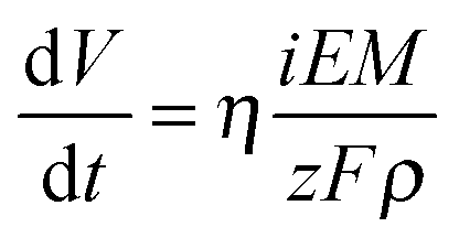
Anodic films were grown to 20 V at 10 mV s−1 on all investigated alloys. In Fig. 1a we report the growth curve in relation to anodizing the Al–91 at% Ta alloy. As typical for valve metals, after an abrupt increase, the current density reaches an almost constant value, which is a function of the metallic substrate composition. The current density is sustained by the oxidation of metals, according to the following half cell reaction:| Me → Mez+ + ze− | (1) |
 | (2) |
 | (3) |
 | ||
| Fig. 1 (a) Current density vs. potential curves recorded during the potentiodynamic growth of anodic films on the Al–91 at% Ta alloy at 10 mV s−1 in 0.1 M ABE. (b) X-Ray reflectivity spectrum in relation to the 20 V anodic film grown on Al–91 at% Ta. Fitting parameters: density = 8.5 g cm−3, thickness = 37 nm, roughness = 0.33 nm. | ||
In Fig. 1b we report the XRR spectrum in relation to the anodic film of Fig. 1a. The resulting angle-dependent curve, which is correlated to the changes in the electron density in the sample, was fitted with a triple layer model (SiO2/alloy/oxide). The fitting procedure allowed estimating a film thickness very close to that estimated from the anodizing ratio (see Table 1), and a density which is very close to that reported for pure anodic Ta2O53 with roughness in the order of few Å. The roughness factor resulted between 0.3 and 0.5 nm for the investigated samples.
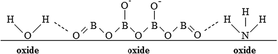
The oxide thickness increases due to the chemical reaction between Ta5+, Al3+, and O2−. Mobile cationic species are produced at the metal/oxide interface and migrate outward toward the oxide/electrolyte interface. Mobile anionic species are produced at the oxide/electrolyte interface and migrate inward. In aqueous solutions, where water molecules might be expected to adhere to the film with negatively charged oxygen atoms adjacent to the oxide surface, mobile anionic species are mainly O2− and OH− ions derived from water de-protonation.14,15 The OH− ions, once incorporated, are converted to O2− ions and protons, with H+ migrating out of the film under the high electric field. If large oxyanions are present in the anodizing bath (e.g. biborate), hydrogen bonds can be formed between H of water molecules and O of such oxyanions (see Scheme 1) with a consequent weakening of O–H covalent bonds in H2O and, thus, easier de-protonation. However, it has been proved that other anionic species, Ay−, of the anodizing bath can also be incorporated during the anodizing process, leading to the formation of oxides containing foreign species.16 Their distribution along the film thickness is a function of the relative migration rate of Ay− with respect to O2−/OH− ions. More specifically, incorporation of several inorganic17 and organic18,19 anions has been reported during anodizing Al, while incorporation of several ions has been proved during anodizing Ta.20 Recently, it has also been demonstrated that N incorporation occurs during anodizing of tantalum in ammonium biborate solutions, provided that the electrolyte pH is higher than the pH of zero charge (pHpzc) of the oxide. In the latter case the oxide surface is negatively charged, thus allowing NH4+ ions to approach the oxide/electrolyte interface and be de-protonated generating NH3−xx− moieties that are incorporated into the anodic film with the consequent formation of an oxynitride.10 In Fig. 2 we report GDOES elemental depth profiles in relation to anodic films grown to 20 V in 0.1 M ABE on Al–10 at% Ta, Al–42 at% Ta and Al–81 at% Ta alloys. The N signal is weak but present across the whole film thickness, thus confirming that nitrogen incorporation also occurs during anodizing Al–Ta alloys. In ref. 21 and 22 pHpzc values of ∼9.5 and 2.9 are reported for alumina and tantala, respectively. Therefore, we expect that the higher is the Al content in the oxide, the lower is the extent of the incorporation phenomena (see Fig. 2).
 | ||
| Scheme 1 | ||
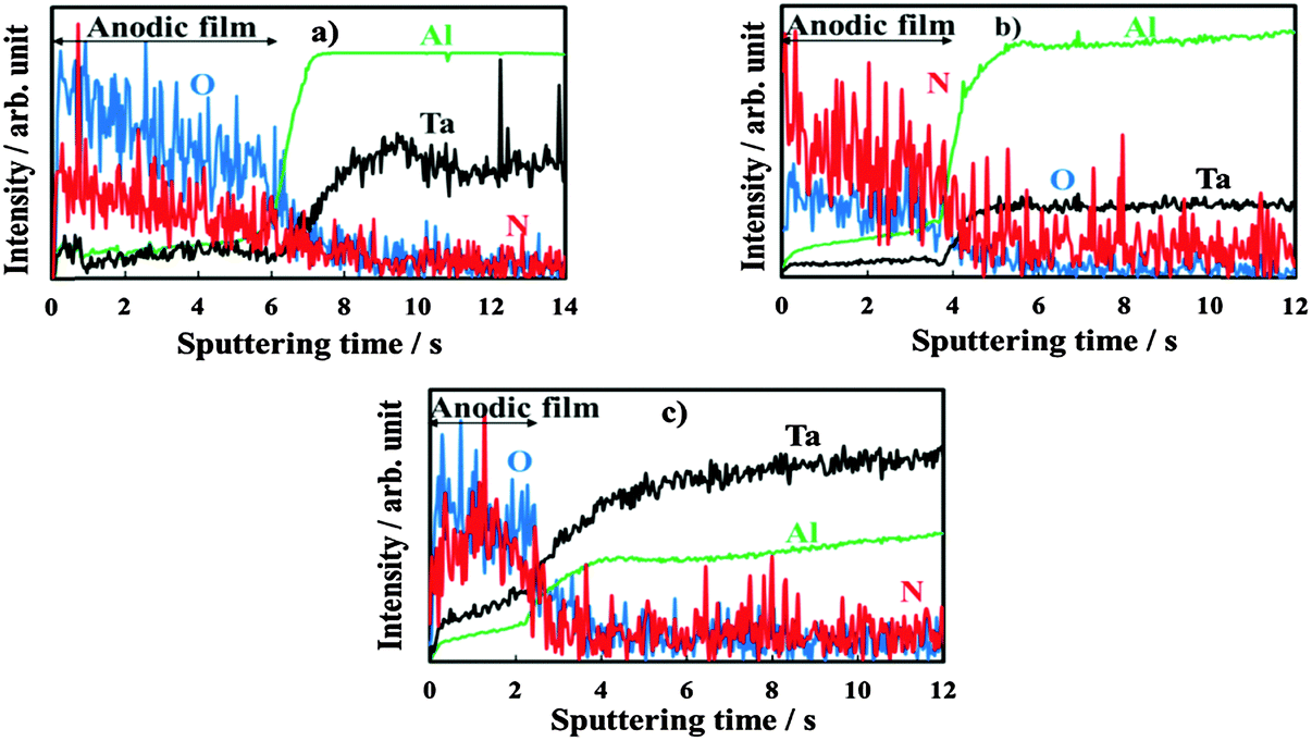 | ||
| Fig. 2 GDOES depth profiles of the anodic films grown to 20 V on (a) Al–10 at% Ta, (b) Al–42 at% Ta and (c) Al–81 at% Ta alloys in 0.1 M ABE. | ||
The formation of NH3−xx− moieties is assisted by weakening the N–H bond as depicted in Scheme 1 since, due to the large electronegativity of nitrogen, the formation of hydrogen bonds between H of ammonia and O of oxyanions (i.e. –NH⋯O) can also occur. As it occurs for OH−, NH3−xx− can lose protons and finally be incorporated into the anodic films as N3− ions. N–H dissociation energy in ammonia (388 kJ mol−1) is lower than O–H dissociation energy in water (463 kJ mol−1). Moreover, ionic radii of NH2− and N3− (0.173 nm and 0.171, respectively, according to ref. 23 and 25) are close to those of O2− and OH− (0.140 nm and 0.153 nm, respectively), and even lower than those of oxyanions, whose incorporation has been proved in previous studies (e.g. 0.238 nm for PO43− and 0.230 nm for SO42−, see ref. 20). Thus, it is likely that an oxynitride can be formed during the anodizing process without significant structural problems, considering that the films are amorphous and that according to the literature the only effect of nitridation of crystalline tantalum oxide is an expansion of the lattice, due to the smaller ionic radius of O2− (0.140 nm) with respect to N3− (0.171 nm).24 Such an expansion is also reported to occur for N-doped Ta2O5 and in spite of this, a crystalline stable phase is formed.
Impedance measurements
In order to obtain information on the dielectric properties of the investigated oxides, we recorded electrochemical impedance spectra and differential capacitance curves. In Fig. 3a–c we report the EIS spectra, recorded in 0.25 M Na2HPO4 at UE = 5 V (Hg/HgO) (i.e. at potentials more anodic than the corresponding flat band potential, see below), in a Modified Bode representation in relation to the anodic films grown on Al–42 at% Ta, Al–62 at% Ta and Al–91 at% Ta alloys, respectively, in 0.1 M ABE and borate buffer to 20 V. As shown in Fig. 3, no significant differences are found in EIS spectra due to the anodizing electrolyte. The high |Z| and a phase angle very close to 90° confirm the formation of blocking oxides. Spectra can be simulated by the electrical circuit reported in Fig. 3d, where Rel is the electrolyte resistance (employed to get the Modified Bode representation), Rox is the anodic film resistance and Qox is a constant phase element (CPE) introduced to model the oxide capacitance.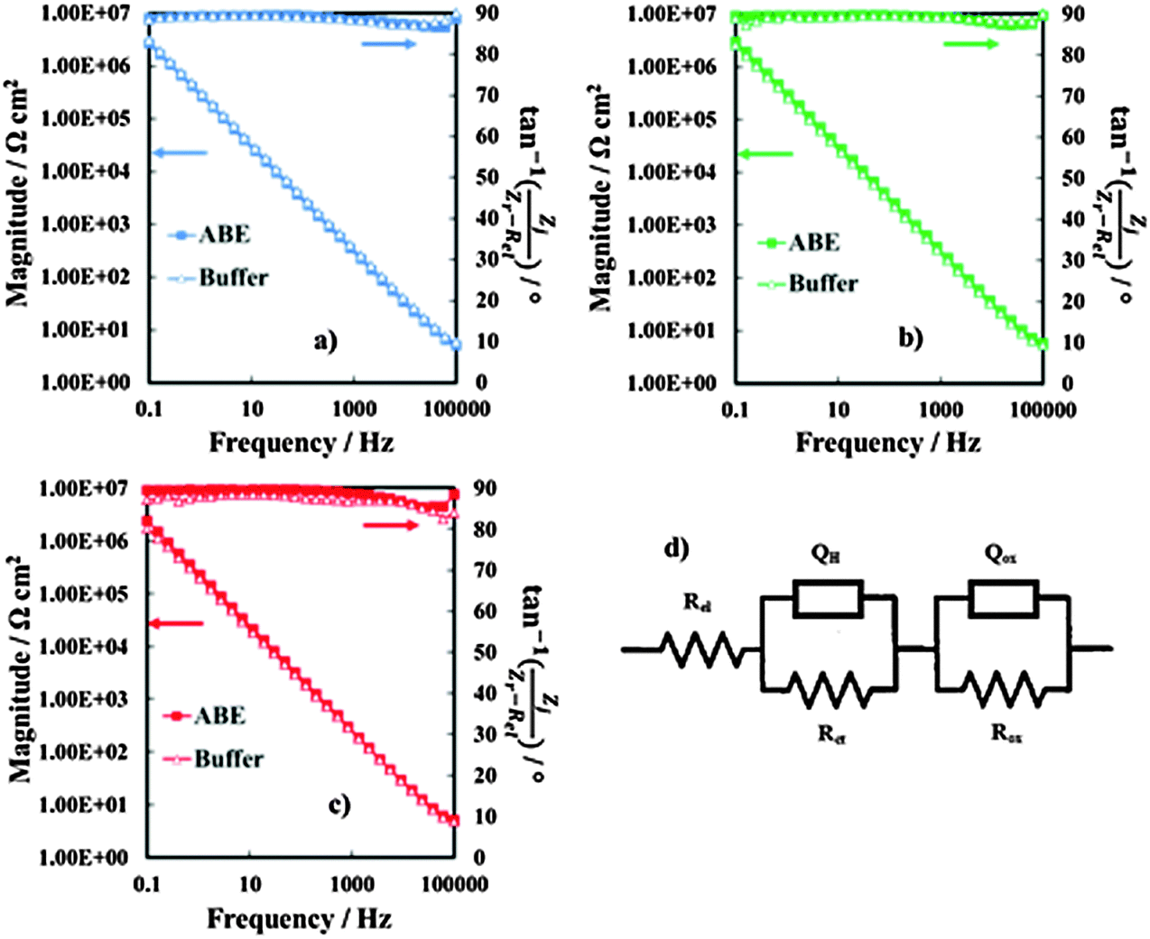 | ||
| Fig. 3 EIS spectra in relation to anodic films grown on (a) Al–42 at% Ta, (b) Al–62 at% Ta and (c) Al–91 at% Ta alloys in ABE and borate buffer, recorded by polarizing the film at 5 V vs. Hg/HgO. (d) Electrical equivalent circuit employed to model metal/oxide/electrolyte interfaces. | ||
Another RQ parallel was inserted to model the electrochemical reaction, where Rct is the charge-transfer resistance and QH the non-ideal Helmholtz double layer capacitance. This equivalent circuit very well fits the experimental data in relation to the all anodic films grown in 0.1 M ABE, with the fitting parameters reported in Table 2. The very high Rox and α values very close to 1 suggest that the oxides behave like ideal capacitors. It is interesting to mention that very high Rct values were estimated, as expected for blocking the interface, and QH allowed estimating the double layer capacitance very close to 20 μF cm−2, the value reported in the literature for aqueous solutions.26
| Base alloy | R el/Ω cm2 | R ct/Ω cm2 | Q H/S sα cm−2 | α | R ox /Ω cm2 | Q ox/S sα cm−2 | α |
|---|---|---|---|---|---|---|---|
| Al | 14 | 1 × 10⁴ | 2.1 × 10⁻⁵ | 0.82 | 1 × 10⁵ | 4.3 × 10⁻⁷ | 1 |
| Al–10 at% Ta | 15 | 1 × 10⁶ | 2.3 × 10⁻⁵ | 0.85 | 1 × 10⁸ | 4.4 × 10⁻⁷ | 0.99 |
| Al–18 at% Ta | 14 | 1 × 10⁶ | 2.1 × 10⁻⁵ | 0.80 | 1 × 10⁸ | 5.4 × 10⁻⁷ | 1 |
| Al–20 at% Ta | 39 | 1 × 10⁶ | 2.4 × 10⁻⁵ | 0.87 | 1 × 10⁹ | 4.2 × 10⁻⁷ | 0.99 |
| Al–30 at% Ta | 26 | 1 × 10⁶ | 2.5 × 10⁻⁵ | 0.88 | 9 × 10⁹ | 4.4 × 10⁻⁷ | 0.99 |
| Al–42 at% Ta | 20 | 1 × 10⁶ | 2.2 × 10⁻⁵ | 0.88 | 1 × 10⁸ | 6.2 × 10⁻⁷ | 0.99 |
| Al–62 at% Ta | 24 | 1 × 10⁶ | 2.2 × 10⁻⁵ | 0.85 | 1 × 10⁸ | 5.4 × 10⁻⁷ | 0.99 |
| Al–81 at% Ta | 23 | 1 × 10⁶ | 2.0 × 10⁻⁵ | 0.82 | 1 × 10⁸ | 7.8 × 10⁻⁷ | 1 |
| Al–91 at% Ta | 27 | 4 × 10⁶ | 2.2 × 10⁻⁵ | 0.95 | 1 × 10⁹ | 6.9 × 10⁻⁷ | 0.99 |
| Ta | 39 | 1 × 10⁶ | 2.2 × 10⁻⁵ | 0.88 | 1 × 10⁸ | 8.5 × 10⁻⁷ | 1 |
In Fig. 4 we report the differential capacitance measurements, recorded at f = 1 kHz, for all the investigated films. It is evident that the capacitance is almost potential independent of and slightly dependent on the frequency, as expected for amorphous insulating materials.26 A comparison with the capacitance of 20 V anodic films on Al–Ta alloys grown in borate buffer solution shows that no appreciable differences are evident on the overall impedance (Fig. 5a–c). This suggests that the presence of N in the oxide causes the formation of deep localized states, thus at the energy level so far from the conduction band mobility edge they cannot contribute to the measured capacitance in the range of investigated frequencies. This is in agreement with previous experimental findings on the effect of nitrogen incorporation during anodizing Ta and Ti,10,11 which is reported to induce the formation of localized states close to the valence band mobility edge.
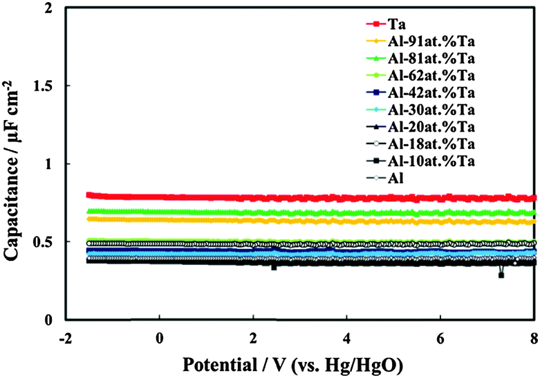 | ||
| Fig. 4 Measured series capacitance in relation to all oxides grown up to 20 V vs. Hg/HgO in ABE. A.c. signal frequency: 1 kHz. | ||
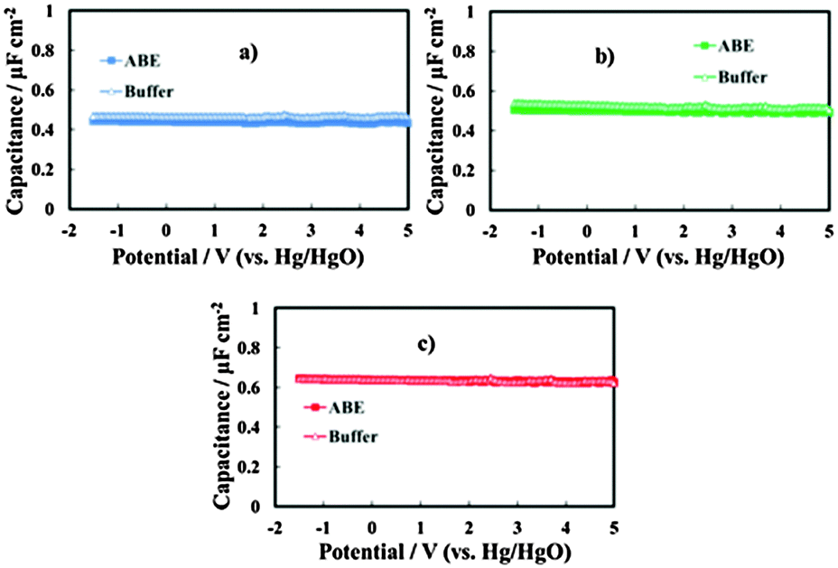 | ||
| Fig. 5 Measured series capacitance in relation to the anodic films grown on (a) Al–42 at% Ta, (b) Al–62 at% Ta and (c) Al–91 at% Ta alloys in ABE and borate buffer. A.c. signal frequency: 1 kHz. | ||
Provided that the equivalent circuit of Fig. 3d simulates well the impedance of the overall metal/oxide/electrolyte interface, it is easy to extract the oxide capacitance from CM. Assuming that Cox can be described by a parallel plate capacitor model:
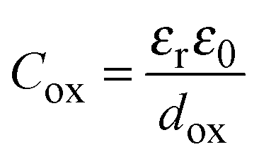 | (4) |
| Base alloy | Dielectric constant |
|---|---|
| Al | 9 |
| Al–10 at% Ta | 10 |
| Al–18 at% Ta | 14 |
| Al–20 at% Ta | 12 |
| Al–30 at% Ta | 13 |
| Al–42 at% Ta | 14 |
| Al–62 at% Ta | 16 |
| Al–81 at% Ta | 24 |
| Al–91 at% Ta | 23 |
| Ta | 29 |
Photoelectrochemical measurements
In order to study the influence of N incorporation on the solid state properties of the oxides, photoelectrochemical measurements were carried out. Anodic photocurrent spectra (normalized for the maximum value of Iph), in relation to the anodic film grown to 20 V on the Al–62 at% Ta alloy in both solutions recorded by polarizing the electrodes at 5 V (Hg/HgO), are reported in Fig. 6a. An evident red-shift in the optical absorption threshold is present for the anodic film grown in 0.1 M ABE, while no photocurrent is detected for λ ≥ 310 nm in the spectrum in relation to the oxide grown in borate buffer. From photocurrent spectra, it is possible to estimate the optical band gap value of the investigated anodic films according to the following equation:| (Iphhν)n ∝ (hν − Eg) | (5) |
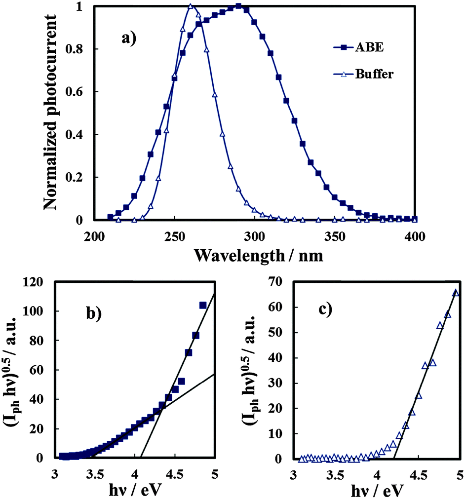 | ||
| Fig. 6 Anodic photocurrent spectra (a) in relation to anodic films grown on the Al–62 at% Ta alloy in ABE and borate buffer, recorded by polarizing the electrodes at 5 V vs. Hg/HgO. The band gap estimate by assuming non-direct optical transitions in relation to the same anodic films grown in ABE (b) and borate buffer (c). | ||
It is important to mention that due to the amorphous structure of the investigated oxides, the presence of allowed localized states inside the gap is predicted according to several models of density of states distribution,12 thus it is more appropriate to define Eg in eqn (5) as the mobility gap of the layer. An Eg of 4.2 eV has been estimated for the anodic film grown in buffer, as shown in Fig. 6c, which is slightly lower than that estimated for thinner oxides (i.e. formation voltage = 10 V).27 For the oxide grown in the ammonium-containing solution (Fig. 6b) by extrapolating the (Iphhν)0.5vs. hν plot to zero it was possible to estimate an Eg of ∼4.1 eV but a long photocurrent tail is also present ending at 3.4 eV.
The latter is due to optical transitions involving the allowed states in the mobility gap of the oxide, generated by N incorporation.
The same photoelectrochemical behaviour was shown by anodic films grown on Al–Ta alloys with a Ta content ≥42 at%, (see Fig. 7), while for the oxide grown on Al–20 at% Ta there is no evidence of photocurrent at energy lower than the Eg of the oxide. We would like to mention that no anodic photocurrent was measured with anodic films grown on Al–Ta alloys with a lower Ta content.
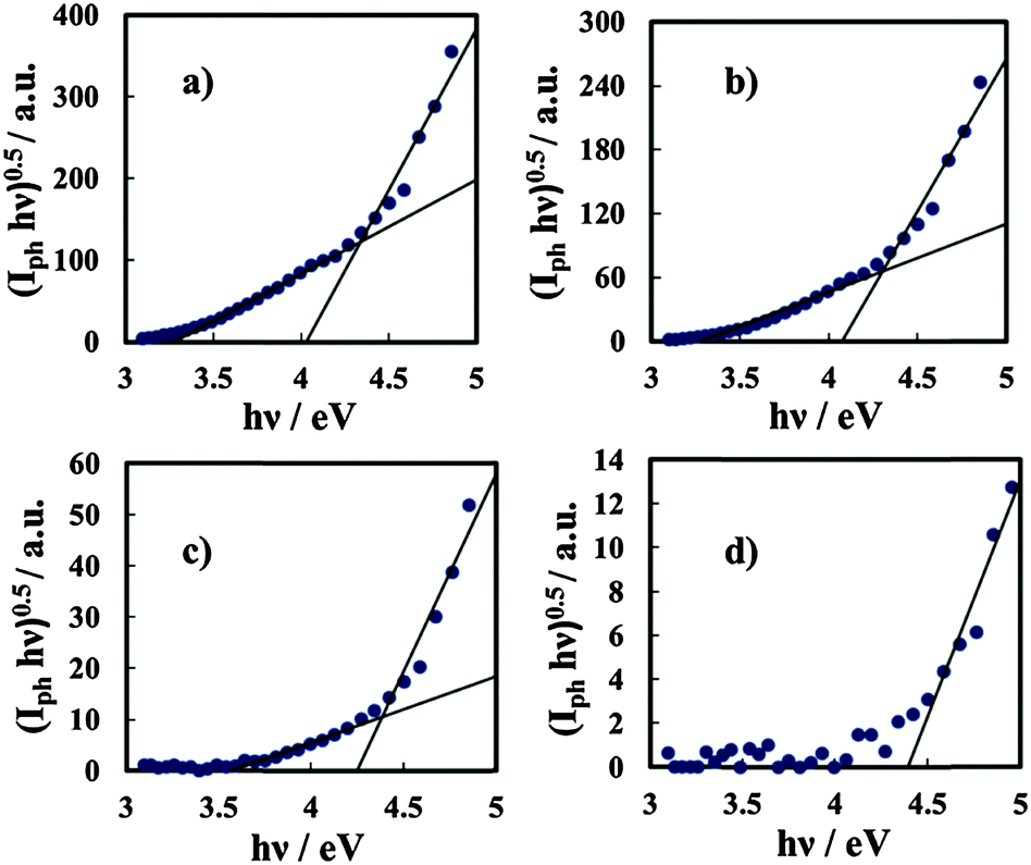 | ||
| Fig. 7 Band gap estimation by assuming non-direct optical transitions in relation to anodic films grown to 20 V on (a) Al–91 at% Ta, (b) Al–81 at% Ta, (c) Al–42 at% Ta, and (d) Al–20 at% Ta alloys in ABE. | ||
We have also studied the dependence of the measured photocurrent on the applied potential, i.e. on the electric field strength across the films. In Fig. 8a we show the Iphvs. UE curves (photocharacteristics) for the anodic films grown on Al–62 at% Ta to 20 V in both ABE and borate buffer, recorded at λ = 270 nm (hν = 4.58 eV). As it will be discussed better in the next section, the shape of Iphvs. UE curves suggests the occurrence of recombination phenomena for both films grown in ABE and borate buffer. As expected for insulating films, by scanning the electrode potential toward the cathodic direction, a clear inversion of the photocurrent sign was revealed, as confirmed by a sharp change in the photocurrent phase angle (not reported).
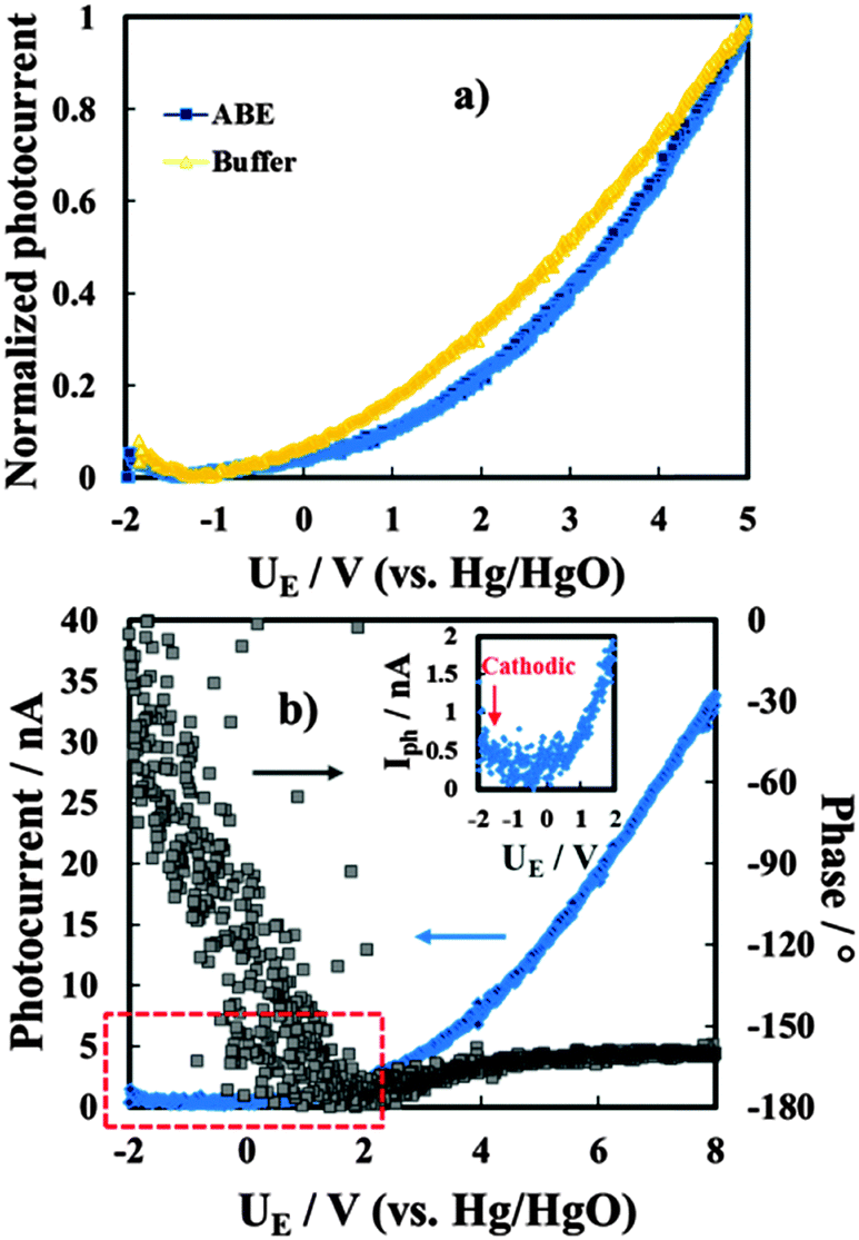 | ||
| Fig. 8 (a) Photocurrent vs. potential curves in relation to 20 V anodic films grown on the Al–62 at% Ta alloy in ABE and borate buffer recorded in 0.1 M ABE at λ = 270 nm. (b) Photocurrent vs. potential curve in relation to the oxide grown on the Al–62 at% Ta alloy in ABE at λ = 330 nm. Potential scan rate: 10 mV s−1. | ||
In the case of the insulating material both anodic and cathodic photocurrents can be measured when the polarizing potential is more anodic and more cathodic than the flat band potential, UFB, of the oxide, respectively.
In order to estimate UFB for the investigated layers, current vs. time measurements were carried out under constant irradiating wavelengths and manually chopping the irradiation. Fig. 9 shows current transients in relation to the anodic film grown on the Al–91 at% Ta alloy in ABE at two different polarizing potentials. Under strong anodic polarization, i.e. at 8 V (Hg/HgO) (Fig. 9a), soon after irradiation the current reaches an almost stationary value for all the investigated wavelengths (up to λ = 360 nm).
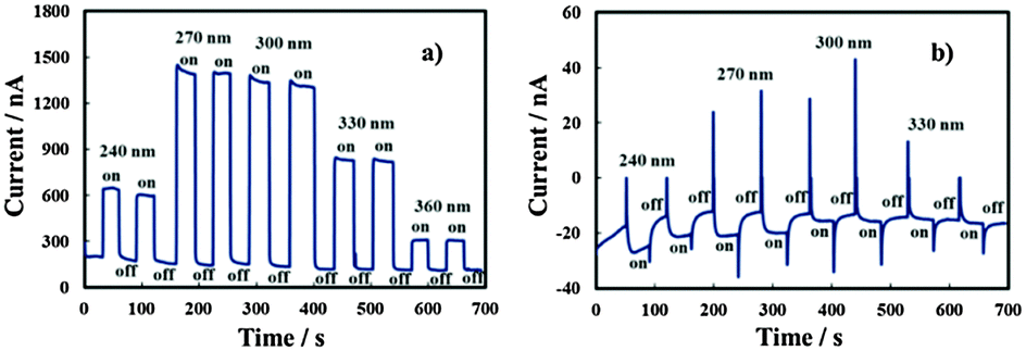 | ||
| Fig. 9 Total current circulating under irradiation (on) and in the dark (off) in the oxide grown on the Al–91 at% Ta alloy in ABE, by polarizing the electrode at 8 V (a) and −0.8 V (b) vs. Hg/HgO at different wavelengths. | ||
At UE = −0.8 V (Hg/HgO) (Fig. 9b), in spite of the presence of anodic photocurrent spikes soon after irradiation, stationary photocurrent is cathodic, thus suggesting UFB > −0.8 V (Hg/HgO). At this electrode potential, the electric field is not high enough to avoid the photocarrier recombination preventing cathodic photocurrent detection at λ = 360 nm, i.e. at photon energy lower than the mobility gap.
U FB values estimated from current–time transients for anodic films grown on alloys with the Ta content ≥62 at% are reported in Table 4. For anodic films grown in 0.1 M ABE with a Ta content ≥62 at%, it was possible to record photocharacteristics under illumination with photons corresponding to hν lower than their mobility gap. In Fig. 8b we show Iphvs. UE at λ = 330 nm (hν = 3.75 eV) for the anodic film grown on Al–62 at% Ta to 20 V in ABE.
| Base alloy | U fb/V (vs. Hg/HgO) |
|---|---|
| Al–62 at% Ta | −0.70 |
| Al–81 at% Ta | −0.75 |
| Al–91 at% Ta | −0.70 |
| Ta | −0.65 |
I ph decreases during the potential scan toward the cathodic direction and for UE < UFB cathodic photocurrent is measured, as evidenced in the magnified area of the plot. Thus, photocurrent spectra were recorded at a potential lower than UFB (i.e. at −1.5 V vs. Hg/HgO), as shown in Fig. 10a for oxides grown on the Al–62 at% Ta alloy in both ABE and borate buffer solutions. As already found for several insulating oxides28–33 as well as for thinner films grown in an ammonium free electrolyte on Al–Ta alloys,27 a long photocurrent tail appears that has been explained by electron injection processes from the alloy Fermi level to the oxide conduction band (see Fig. 10d).
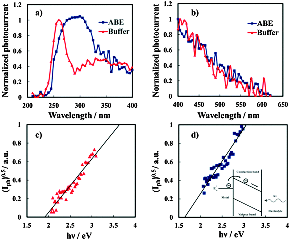 | ||
| Fig. 10 (a) Cathodic photocurrent spectra in relation to the oxides grown on the Al–62 at% Ta alloy in ABE and borate buffer recorded at −1.5 V vs. Hg/HgO as an electrode potential. (b) Long wavelength region of the photocurrent spectra, recorded by using a UV filter. Fowler plots in relation to the oxide grown in buffer (c) and ABE (d). Inset: Internal photoemission of electrons from the metal Fermi level. | ||
The threshold energy, Eth, associated with this process can be estimated according to Fowler's law:28
| (Iph)0.5 ∝ (hν − Eth) | (6) |
Discussion
In the framework of Butler–Gartner model, for crystalline insulating films, a linear dependence of the measured photocurrent on the applied potential is expected in the absence of trapping phenomena, which can modify the electric field distribution across the layer.34However, for both anodic films grown in ABE and buffer, such dependence is not linear thereby supporting the presence of recombination phenomena. For amorphous materials the lack of a long range order induces the formation of allowed localized states close to the mobility edge of the oxide, in agreement with the Mott and Davis model.35 Thus, together with surface and bulk recombination phenomena expected for both crystalline and amorphous materials, we have to account for the occurrence of geminate recombination phenomena which reduce the efficiency of free carrier generation for amorphous anodic films on Al–Ta alloys. Geminate recombination occurs generally in any material where the photogenerated carriers display very low mobility.
The mobility of carriers in the localized states (below the conduction band and above the valence band edges) is much lower than in the extended states, so the probability of initial recombination effects in amorphous materials is quite high.
In fact, during the thermalization time, the electron–hole pairs do not cover a distance long enough to prevent recombination due to their mutual coulombic attraction. Owing to this insufficient separation, a certain fraction of the photogenerated carriers recombine before the transport process can separate them permanently.36,37
To explain the dependence of photocurrent on both the applied potential and the irradiating wavelength, we recall Onsager's theory,38 originally developed for weak electrolytes, and then applied by Pai and Enck to the initial recombination process (geminate recombination) of electron–hole pairs in amorphous selenium.39 This was achieved by deriving a mathematical expression for the efficiency of photogeneration, ηg, taking into account the tri-dimensional aspect of the generation and the effect of the electric field on the initial separation of the photocarriers:
 | (7) |
 | (8) |
| LD = (μhτh + μeτe)E | (9) |
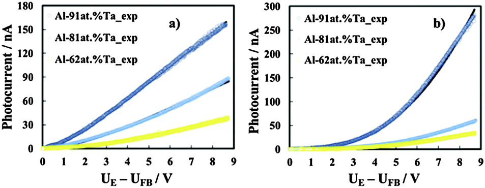 | ||
| Fig. 11 Photocurrent vs. band bending in relation to anodic films grown to 20 V on Al–91 at% Ta, Al–81 at% Ta, and Al–62 at% Ta alloys in ABE, recorded at λ = 240 nm (a) and λ = 330 nm (b). Continuous lines are plotted according to eqn (8) with the fitting parameters of Table 5. | ||
The reflection coefficient has been calculated by using a three-layer model (i.e. solution/oxide/metal) under normal light incidence and by including the effects of multiple reflections,40 with optical constants for solution, metal and oxide taken from ref. 41 and 42. During the fitting procedure we used the flat band potentials estimated from current time transients (see Table 4) and oxides' thickness calculated from the anodizing ratio estimated in ref. 3 and 4 by direct inspection of transmission electron micrographs of the ultramicrotomed section (see Table 1).
The best fitting parameters are summarized in Table 5. It is interesting to mention that r0 is inversely proportional to the wavelength, and that very low μτ values were derived from the best fitting procedure. This suggests that for λ corresponding to both supra- and sub-band gap values, photocarriers are generated in localized states. Due to the amorphous nature of the investigated anodic films, we expect that close to the conduction and valence band mobility edges, lattice disorder and/or the presence of not stoichiometric oxides induce the formation of localized states, which can extend up to 0.2 eV below CB and above VB edges.30 For hν < Eg we can conclude that the allowed localized states are also present inside the mobility gap and μτ even lower than that estimated for the higher irradiating wavelength suggests that they are strongly localized.
| Base alloy | Wavelength/nm | μτ/cm2 V−1 | r 0/Å |
|---|---|---|---|
| Al–62 at% Ta | 240 | 6.7 × 10⁻¹⁵ | 10 |
| 270 | 3.7 × 10⁻¹⁵ | 7.5 | |
| 300 | 9.2 × 10⁻¹⁶ | 7 | |
| 330 | 4.8 × 10⁻¹⁶ | 6 | |
| Al–81 at% Ta | 240 | 1.3 × 10⁻¹⁴ | 10 |
| 270 | 1.0 × 10⁻¹⁴ | 6 | |
| 300 | 3.7 × 10⁻¹⁵ | 4.5 | |
| 330 | 1.9 × 10⁻¹⁵ | 4 | |
| Al–91 at% Ta | 240 | 2.3 × 10⁻¹⁴ | 14 |
| 270 | 2.1 × 10⁻¹⁴ | 7 | |
| 300 | 1.0 × 10⁻¹⁴ | 5 | |
| 330 | 9.0 × 10⁻¹⁵ | 4 | |
| Ta | 240 | 2.4 × 10⁻¹⁴ | 17.5 |
| 270 | 1.9 × 10⁻¹⁴ | 6 | |
| 300 | 9.0 × 10⁻¹⁵ | 4 | |
| 330 | 7.7 × 10⁻¹⁵ | 3 | |
If we recall that Fowler threshold energies for films grown in borate buffer and films grown in ABE are almost coincident and that N incorporation does not contribute significantly to the measured impedance, we can suggest that anodizing in ABE leads to the formation of anodic films whose density of states can be described according to the sketch of Fig. 12.
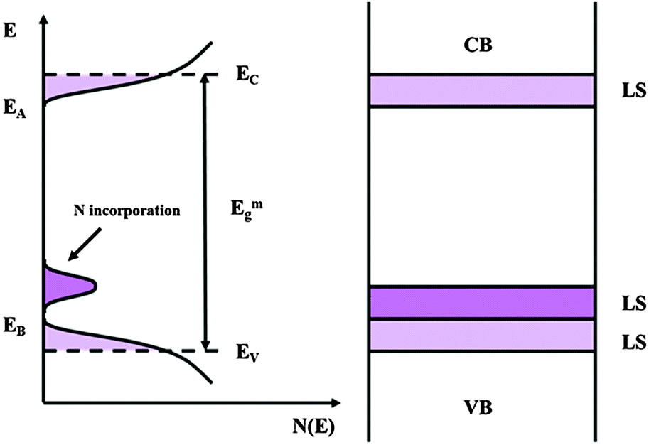 | ||
| Fig. 12 Electronic structure of amorphous semiconducting oxides following the Mott–Davis model with allowed localized states in the mobility gap. LS: localized states. | ||
N incorporation induces the formation of allowed localized states close to the valence band mobility edge of the oxides, and that the energy distance of such states from the conduction band mobility edge is roughly correlated to the red-shift of the light absorption threshold of the anodic spectra.
Conclusions
Anodic films were grown to 20 V on sputtering-deposited Al–Ta alloys of several compositions in 0.1 M ABE and borate buffer solutions. According to GDOES compositional depth profiles, anodizing in ABE leads to the formation of N containing oxide layers with nitrogen distributed across the whole film thickness. The presence of N does not change appreciably the impedance of the oxides, as suggested by the comparison between the impedance spectra and the differential capacitance curves in relation to anodic films grown in ammonium-free and ammonium-containing solutions. In contrast, N incorporation significantly changes the photoelectrochemical behaviour of the anodic films grown on Al–Ta alloys with the Al content ≥20 at%. A red-shift of the light absorption threshold of the investigated layers was evidenced, which is attributed to the optical transition involving allowed states inside the mobility gap of the films. The dependence of photocurrent on photon energy and the electric field strength in the framework of Pai–Enck model for geminate recombination suggested that incorporation of nitrogen induces the formation of allowed localized states. Such states are close to the valence band mobility edge, since they do not contribute to the measured impedance up to a very low frequency of the a.c. signal (0.1 Hz) and since they do not affect the Fowler threshold for the internal electron photoemission phenomena.Notes and references
- G. Scaduto, M. Santamaria, P. Bocchetta and F. Di Quarto, Thin Solid Films, 2014, 550, 128 CrossRef CAS.
- S. Ezhilvalavan and T. Y. Tseng, J. Mater. Sci.: Mater. Electron., 1999, 10, 9 CrossRef CAS.
- H. Habazaki, K. Shimizu, P. Skeldon, G. E. Thompson and G. C. Wood, Proc. R. Soc. A, 1997, 453, 1593 CrossRef CAS.
- G. Alcalá, S. Mato, P. Skeldon, G. E. Thompson, P. Bailey, T. C. Q. Noakes, H. Habazaki and K. Shimizu, Corros. Sci., 2003, 45, 1803 CrossRef.
- G. Alcalá, P. Skeldon, G. E. Thompson, A. B. Mann, H. Habazaki and K. Shimizu, Nanotechnology, 2002, 13, 451 CrossRef.
- S. J. Garcia-Vergara, I. S. Molchan, F. Zhou, H. Habazaki, D. Kowalski, P. Skeldon and G. E. Thompson, Surf. Interface Anal., 2011, 43, 893 CrossRef CAS.
- F. Zhou, D. J. Leclere, S. J. Garcia-Vergara, T. Hashimoto, I. S. Molchan, H. Habazaki, P. Skeldon and G. E. Thompson, J. Electrochem. Soc., 2010, 157, C437 CrossRef CAS.
- H. Habazaki, K. Shimizu, S. Nagata, P. Skeldon, G. E. Thompson and G. C. Wood, Corros. Sci., 2002, 44, 1047 CrossRef CAS.
- S. Ono, K. Kuramochi and H. Asoh, Corros. Sci., 2009, 51, 1513 CrossRef CAS.
- F. Di Franco, M. Santamaria, F. Di Quarto, E. Tsuji and H. Habazaki, Electrochim. Acta, 2012, 59, 382 CrossRef CAS.
- S. Miraghaei, M. Santamaria and F. Di Quarto, Electrochim. Acta, 2014, 134, 150 CrossRef CAS.
- (a) F. Di Quarto, F. La Mantia and M. Santamaria, in Modern Aspects of Electrochemistry, No. 46: Progress in Corrosion Science and Engineering I, ed. S.-I. Pyun and J.-W. Lee, Springer, New York, 2009, ch. 4, pp. 231–316 Search PubMed; (b) F. La Mantia, M. Santamaria, F. Di Quarto and H. Habazaki, J. Electrochem. Soc., 2010, 157, C258 CrossRef CAS.
- M. Pourbaix, Atlas of electrochemical equilibria in aqueous solutions, Pergamon Press, Oxford, UK, 1966 Search PubMed.
- Oxides and Oxide Films, ed. J. W. Diggle, Marcel Dekker, Inc., New York, 1973 Search PubMed.
- A. J. Brock and G. C. Wood, Electrochim. Acta, 1967, 12, 395 CrossRef.
- H. Habazaki, K. Fushimi, K. Shimizu, P. Skeldon and G. E. Thompson, Electrochem. Commun., 2007, 9, 1222 CrossRef CAS.
- G. C. Wood, P. Skeldon, G. E. Thompson and K. Shimizu, J. Electrochem. Soc., 1996, 143, 74 CrossRef CAS.
- F. Di Quarto, S. Piazza, A. Splendore and C. Sunseri, Proceedings of the Symposium on Oxide Films on Metals and Alloys, The Electrochemical Society, Inc., Pennington, 1992 Search PubMed.
- K. Shimizu, H. Habazaki, P. Skeldon, G. E. Thompson and G. C. Wood, Electrochim. Acta, 2001, 46, 4379 CrossRef CAS.
- K. Shimizu, K. Kobayashi, G. E. Thompson, P. Skeldon and G. C. Wood, Philos. Mag. B, 1996, 73, 461 CrossRef CAS.
- E. McCafferty, Electrochim. Acta, 2010, 55, 1630 CrossRef CAS.
- E. McCafferty, J. Electrochem. Soc., 1999, 146, 2863 CrossRef CAS.
- A. F. Wells, Structural Inorganic Chemistry, Clarendon Press, Oxford, UK, 1975 Search PubMed.
- A. Dabirian and R. Van de Krol, Chem. Mater., 2015, 27, 708 CrossRef CAS.
- P. W. Atkins, The Elements of Physical Chemistry, Oxford University Press, Oxford, UK, 1996 Search PubMed.
- (a) F. Di Franco, M. Santamaria, F. Di Quarto, F. La Mantia, C. M. Rangel and A. I. De Sá, ECS J. Solid State Sci. Technol., 2013, 11, N205 CrossRef; (b) F. Di Franco, G. Zampardi, M. Santamaria, F. Di Quarto and H. Habazaki, J. Electrochem. Soc., 2012, 159, C33 CrossRef CAS; (c) F. La Mantia, H. Habazaki, M. Santamaria and F. Di Quarto, Russ. J. Electrochem., 2010, 46, 1306 CrossRef.
- A. Zaffora, F. Di Franco, M. Santamaria, H. Habazaki and F. Di Quarto, Electrochim. Acta, 2015, 180, 666 CrossRef CAS.
- M. Santamaria, F. Di Quarto and H. Habazaki, Electrochim. Acta, 2008, 53, 2272 CrossRef CAS.
- F. Di Quarto, M. Santamaria, P. Skeldon and G. E. Thompson, Electrochim. Acta, 2003, 48, 1143 CrossRef CAS.
- M. Santamaria, F. Di Quarto, P. Skeldon and G. E. Thompson, J. Electrochem. Soc., 2006, 153, B518 CrossRef CAS.
- M. Santamaria, F. Di Quarto, S. Zanna and P. Marcus, Electrochim. Acta, 2011, 56, 10533 CrossRef CAS.
- M. Santamaria, F. Di Quarto, S. Zanna and P. Marcus, Electrochim. Acta, 2007, 53, 1315 CrossRef.
- M. Santamaria, F. Di Franco, F. Di Quarto, P. Skeldon and G. E. Thompson, J. Phys. Chem. C, 2013, 117, 4201 CAS.
- F. Di Quarto, F. Di Franco, C. Monarca, M. Santamaria and H. Habazaki, Electrochim. Acta, 2013, 110, 517 CrossRef CAS.
- N. F. Mott and E. A. Davis, Electronic Processes in Non-crystalline Materials, Clarendon Press, Oxford, UK, 2nd edn, 1979 Search PubMed.
- M. Santamaria, F. Di Quarto and H. Habazaki, Corros. Sci., 2008, 50, 2012 CrossRef CAS.
- F. Di Quarto, S. Piazza, M. Santamaria and C. Sunseri, in Handbook of Thin Film Materials, ed. H. S. Nalwa, Academic Press, New York, 2002, vol. 2, ch. 8, pp. 373–414 Search PubMed.
- (a) L. Onsager, J. Chem. Phys., 1934, 2, 599 CrossRef CAS; (b) L. Onsager, Phys. Rev., 1938, 54, 554 CrossRef CAS.
- D. M. Pai and R. C. Enck, Phys. Rev. B: Solid State, 1975, 11, 5163 CrossRef CAS.
- O. S. Heavens, Optical Properties of Thin Solid Films, Dover Publications, New York, 1965 Search PubMed.
- CRC Handbook of Chemistry and Physics, ed. D. R. Lide, CRC Press/Taylor and Francis, Boca Raton, 90th edn, 2010 Search PubMed.
- S. Adachi, The Handbook on Optical Constants of Metals, World Scientific, 2012 Search PubMed.
Footnote |
| † Electronic supplementary information (ESI) available. See DOI: 10.1039/c5cp04347f |
| This journal is © the Owner Societies 2016 |