
 Open Access Article
 This Open Access Article is licensed under a
 Creative Commons Attribution 3.0 Unported Licence
Grain rotation and lattice deformation during perovskite spray coating and annealing probed in situ by GI-WAXS†
S.
Lilliu
 *a,
J.
Griffin
a,
A. T.
Barrows
a,
M.
Alsari
b,
B.
Curzadd
c,
T. G.
Dane
d,
O.
Bikondoa
e,
J. E.
Macdonald
f and
D. G.
Lidzey
a
*a,
J.
Griffin
a,
A. T.
Barrows
a,
M.
Alsari
b,
B.
Curzadd
c,
T. G.
Dane
d,
O.
Bikondoa
e,
J. E.
Macdonald
f and
D. G.
Lidzey
a
aDepartment of Physics and Astronomy, University of Sheffield, Sheffield, S3 7RH, UK. E-mail: samuele_lilliu@hotmail.it; s.lilliu@sheffield.ac.uk; d.g.lidzey@sheffield.ac.uk
bCavendish Laboratory, University of Cambridge, CB30HE Cambridge, UK
cDepartment of Mechanical Engineering, Technische Universität München, 85748 München, Germany
dEuropean Synchrotron Radiation Facility, BP 220, F-38043 Grenoble, France
eDepartment of Physics, University of Warwick, CV4 7AL Coventry, UK
fSchool of Physics and Astronomy, Cardiff University, CF24 3AA Cardiff, UK
First published on 2nd June 2016
Abstract
We report for the first time on grain rotation in CH3NH3PbI3 perovskite films for ∼12% efficient planar solar cells and present a new method for investigating their texture evolution during thermal annealing. Our technique is based on in situ 2D grazing incidence wide-angle X-ray scattering (GI-WAXS) and employs a 10 keV wide-focussed X-ray beam to simultaneously probe a large number of grains. The ability to track the texture dynamics from a statistically relevant number of spots diffracting from single grains during thermal annealing and in grazing incidence geometry can have applications understanding the processing dynamics of a range of new materials.
Introduction
Solution-processed mixed lead halide perovskites are promising candidates for opto-electronic devices.1–7 In devices such as planar heterojunction solar cells, the perovskite layer can be deposited from a precursor solution of methylammonium iodide (MAI, MA = CH3NH3) and PbCl2 (3![[thin space (1/6-em)]](https://www.rsc.org/images/entities/char_2009.gif) :1 mol) in dimethylformamide (DMF).5,8 Thermal annealing above 80 °C enables the conversion of the as-deposited polycrystalline precursor film to a polycrystalline MAPbI3 perovskite, which is composed of platelet-like grains or crystallites separated by grain boundaries.9,10 Recent results suggest that perovskite opto-electronic properties can be optimized by favouring the formation of large grains and, thus, minimizing grain boundaries.11–14 Although grains can be visualized by transmission electron microscopy (TEM) and scanning electron microscopy (SEM), these measurements cannot be integrated with in situ solution deposition nor with in situ annealing under ambient conditions. Complex synchrotron 2D diffraction techniques based on hard X-rays, highly focussed beams, and transmission geometry, such as 3DXRD,15,16 are also unsuitable. In fact, they can only illuminate a limited number of grains (limited number of diffraction spots on the same image),17 are not fast enough to investigate the structural changes that occur during the annealing of MAPbI3, and induce excessive beam damage. Here we show that a statistically relevant characterisation of the slow dynamics of precursor and perovskite crystallites can be achieved with a simple setup. By employing standard synchrotron beamline optics, a beam spot size of ∼500 × 100 μm2 and a 2D detector, we measured thousands of highly resolved diffraction spots from single crystallites by in situ grazing incidence wide-angle scattering (GI-WAXS). This allowed us to follow grain rotation and lattice deformation within a MAPbI3 precursor and perovskite in real-time as the sample was annealed.
:1 mol) in dimethylformamide (DMF).5,8 Thermal annealing above 80 °C enables the conversion of the as-deposited polycrystalline precursor film to a polycrystalline MAPbI3 perovskite, which is composed of platelet-like grains or crystallites separated by grain boundaries.9,10 Recent results suggest that perovskite opto-electronic properties can be optimized by favouring the formation of large grains and, thus, minimizing grain boundaries.11–14 Although grains can be visualized by transmission electron microscopy (TEM) and scanning electron microscopy (SEM), these measurements cannot be integrated with in situ solution deposition nor with in situ annealing under ambient conditions. Complex synchrotron 2D diffraction techniques based on hard X-rays, highly focussed beams, and transmission geometry, such as 3DXRD,15,16 are also unsuitable. In fact, they can only illuminate a limited number of grains (limited number of diffraction spots on the same image),17 are not fast enough to investigate the structural changes that occur during the annealing of MAPbI3, and induce excessive beam damage. Here we show that a statistically relevant characterisation of the slow dynamics of precursor and perovskite crystallites can be achieved with a simple setup. By employing standard synchrotron beamline optics, a beam spot size of ∼500 × 100 μm2 and a 2D detector, we measured thousands of highly resolved diffraction spots from single crystallites by in situ grazing incidence wide-angle scattering (GI-WAXS). This allowed us to follow grain rotation and lattice deformation within a MAPbI3 precursor and perovskite in real-time as the sample was annealed.
Results and discussion
Measurements were performed at the XMaS beamline (ESRF) with a chamber equipped with a spray coater and an annealing stage. The MAI:PbCl2 (3:1 mol in DMF) precursor solution was spray coated in situ on a 1 cm2 Si/SiO2 substrate placed on a preheated (60 °C) annealing stage for a period of 10 minutes.5 Annealing was then performed under the same conditions on a preheated (110 °C) annealing stage for 94 min. During both the initial deposition process and the subsequent anneal, diffraction images were collected above the critical angle (αi = 0.3°, corresponding to a penetration depth of ∼150 nm).
Fig. 1 shows 2D GI-WAXS images of the spray coated precursor and perovskite phases with azimuthally integrated line profiles,10 illustrating the structural evolution that takes place during deposition and annealing. The full sequence of images recorded during deposition and annealing is shown in Videos 1 and 2 (ESI†) respectively.
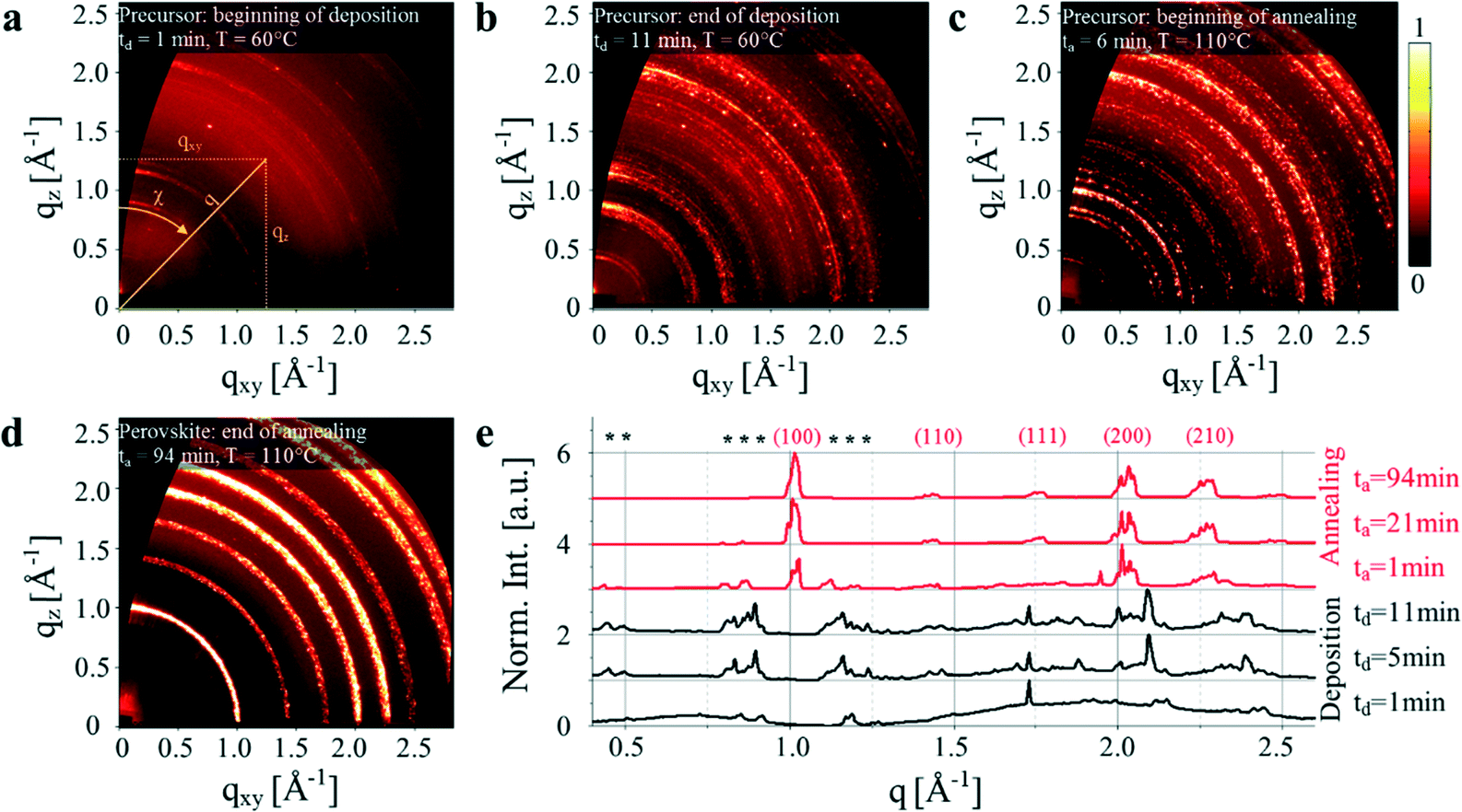 | ||
| Fig. 1 GI-WAXS images (a–d) showing the isothermal evolution of MAI:PCl2 (3:1 mol in DMF) following in situ spray coating at 60 °C on a Si/SiO2 substrate followed by in situ thermal annealing at 110 °C. td and tA indicate deposition and annealing time, respectively. e, azimuthally integrated line profiles at different instants showing the structural evolution. Precursor peaks are indicated with black symbols (*), perovskite peaks are indexed in red. | ||
Here images are represented in reduced scattering vector rectangular coordinates qz and qxy, where 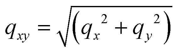 and qx, qy, qz are the scattering vector components. We also employ scattering vector polar coordinates q and χ, where q is the distance and χ is the azimuthal angle (see inset in a). The polycrystalline film evolves during deposition and annealing over a number of stages.10 Following the deposition of the precursor solution, the evaporation of solvent leads to the formation of a precursor polycrystal; a process accompanied by a simultaneous transition of the precursor to a perovskite together with perovskite crystallization.10 After extended annealing, such perovskites undergo degradation. Specifically, following the first moments after deposition, two broad peaks are visible over the scattering vector range q = [0.5−1] and [1.5−2.5] Å−1 that originate from the presence of the casting solvent (see Fig. 1e, deposition time td = 1 min). As the solvent evaporates, the precursor crystals nucleate and crystallise (Fig. 1b).10 At the beginning of the anneal (Fig. 1c) the precursor peaks are still visible, however at annealing time ta = 94 min (Fig. 1d) these features are no longer evident and have been replaced by peaks characteristic of the perovskite. As the measurements reported here were performed at 60 °C (deposition) and 110 °C (anneal), we index the perovskite features according to its previously reported cubic structure.5,21–24 Interestingly, it can be seen that the diffraction rings are composed of a large number of individual diffraction spots, resulting from diffraction by single crystallites. From the sequence of images shown in Videos 1 and 2 (ESI†), it can be seen that while most of these spots are stationary, hundreds of them move azimuthally during the deposition and the annealing process, indicating that the corresponding diffracting crystallites undergo rotation or reorientation.
Note that further GI-WAXS measurements performed on films spin coated from the precursor solutions described here, and annealed under different atmosphere and different annealing temperatures were used to explore the dependence of grain rotation on film preparation conditions (see Videos 3–11, ESI†). We observed grain rotation in perovskite films spin coated under conditions that are similar to the ones followed during solar cell fabrication, in which we typically achieve ∼12% power conversion efficiency (see Fig. S1 and Table S1, ESI†). Our GI-WAXS measurements suggest that the amount of rotating diffraction spots visible on the diffraction patterns increase with increasing amount of humidity or, equivalently, a higher level of precursor film hydration (see Fig. S2, ESI†). Indeed, the density of rotating spots observed in the spray coated films is enhanced compared to spin coated films as spray coated films are often slightly coarser and more porous.
To understand the grain rotation process in more detail, we have implemented a spot tracking routine to follow several of the moving diffraction spots. Here, we extract a series of ‘tracks’ that quantify the scattering vector of each spot along with its time coordinates. Videos 12 and 13 (ESI†) show 32 and 601 tracks detected during the spray coating and annealing phases respectively. We find that diffraction spots appear, move and then disappear, and thus the number of detected tracks varies as a function of time (the diffraction spots that move continuously are reorienting by rotation around an axis approximately parallel to the incident beam, while the diffraction spots that appear and disappear rapidly are rotating around other axes). As the precursor film dries, the number of tracks increase monotonically, indicating that the number of moving precursor grains increases as the solvent evaporates (see Fig. S3, ESI†). Note that one of the limitations of our method is that we are unable to associate different diffraction spots from different Miller planes belonging to the same crystallite. This would require acquiring multiple diffraction patterns at different ω sample orientations (with the rotation axis perpendicular to the substrate) with a fine Δω step size during the in situ annealing, as in 3DXRD.18,19 However, while this measurement could be possible with a fast detector, it would not be compatible with our experimental setup and with a grazing incidence geometry, and would be certainly complicated by the fact that the diffraction spots move during annealing.
Fig. 2a and b show tracks detected during the anneal and then assigned to either the precursor or perovskite phase according to their location in the diffraction pattern. As shown in Fig. 2c, the number of precursor tracks reaches a maximum at ta ≈ 6 min and then decreases monotonically to zero, whereas the number of perovskite tracks reaches a quasi-constant value within 30 min after the start of the annealing.
 | ||
| Fig. 2 Real-time observation of precursor and perovskite crystallite rotation. a, Detected precursor tracks at 6 min since the beginning of the annealing. b, Detected perovskite tracks at the end of the annealing (94 min). c, Number of detected tracks vs. time. d, Sequence of images showing a precursor spot rotation. e, Scattering vector polar coordinates of the track shown in d. f, Sequence of images showing a perovskite track rotation near (210). g, Scattering vector polar coordinates of the track shown in f. | ||
The fact that we see two populations of tracks that have different dynamics suggest that the motion of such tracks is not activated by the X-ray beam.16 Our measurements thus indicate that precursor grains are formed within the first 6 min of the experiment and subsequently undergo thermally activated conversion to the perovskite in time-scales between 6 and 70 min.
Fig. 2d–f show exemplary precursor and perovskite tracks, with their scattering vector polar coordinates plotted in Fig. 2e–g, respectively. Here, the azimuthally elongated shape is due to a combination of the spot moving during the acquisition of a single image and possibly the grain itself changing shape. The precursor track (Fig. 2d and e) shows a monotonic negative azimuthal displacement, which indicates a continuous counterclockwise rotation of the precursor grain. The distance displacement is less regular (corresponding to a lattice contraction followed by an expansion) and is weakly correlated with the azimuthal displacement.
In contrast, the perovskite track (Fig. 2f and g) located on the (210) ring undergoes a continuous positive azimuthal displacement that is negatively correlated to its distance displacement. It appears therefore that in this case, a clockwise rotation is accompanied by a tiny lattice expansion. We find that this movement ceases at 26 minutes after the beginning of the annealing however this track does not disappear from the images.
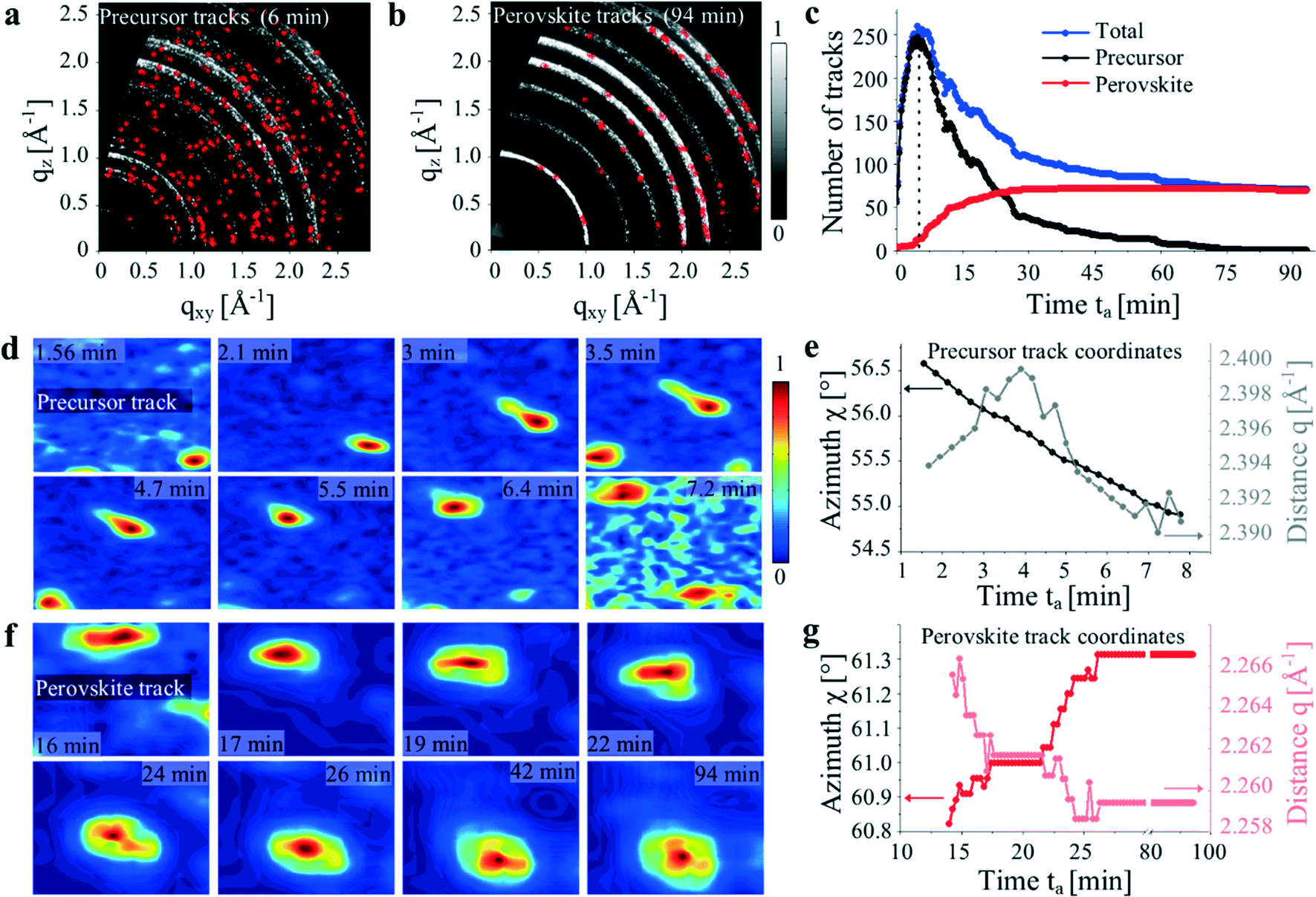
We now turn our attention to the collective behaviour of the 601 grains that move during the annealing process. Fig. 3a and b shows azimuth (Δχ) and distance (Δq) displacement vs. annealing time for all the tracks.
 | ||
| Fig. 3 Precursor (black) and perovskite (red) tracks extracted from the annealing dataset and clustered. a, Azimuth displacement Δχ vs. time for 529 precursor tracks (red) and 72 perovskite tracks (black). b, Distance displacement Δq vs. time for 529 precursor tracks and 72 perovskite tracks. c–f, Δq vs. Δχ precursor and perovskite curves clustered into four groups with two self-organizing maps (SOM). Cluster 1 is the dataset representing grains rotating clockwise and contracting. Cluster 2 represents grains rotating counterclockwise and contracting. Cluster 3 represents grains rotating counterclockwise and expanding. Cluster 4 represents grains rotating clockwise and expanding. | ||
Typical Δχ curves display a trend described by A × (1 − e−t/Δt), where A is the maximum value of the azimuth displacement, t is the time, and Δt is a characteristic time constant. We find that grains rotate both clockwise (Δχ > 0) and counterclockwise (Δχ < 0) with around 58% of precursor and perovskite grains preferentially rotating counterclockwise (see Fig. S4, ESI†). The maximum value of Δχ is greater for the precursor tracks than for the perovskite tracks.
As shown in Fig. S5 (ESI†), most of the precursor tracks start moving at ta,start ∼ 7.0 min and then stop and disappear at ta,end ∼ 15 min. Perovskite spots appear ∼5 min later, move more slowly (see ta,rise), and can be detected over the entire annealing process. The mean instantaneous velocity (Δχ/t) is roughly the same for tracks moving clockwise and counterclockwise (Fig. S6, ESI†).
Finally, the mean value of χ per track is distributed uniformly over the angle range 30° to 70° (Fig. S7, ESI†), indicating that the rotating grains are evenly distributed in the diffraction patterns. In the exemplary tracks shown in Fig. 2e–g it can be seen that the χ and q profiles can be positively or negatively correlated. A statistical analysis presented in Fig. S8 to S10 (ESI†) of the cross correlation coefficient between Δχ and Δq shows that the total number of positively correlated tracks is ∼54% and that most of the Δχ and Δq profiles are highly correlated.
We further classify precursor and perovskite tracks by training two self-organizing maps (SOMs) in MATLAB (see Fig. S11 and S12, ESI†).20Fig. 3d shows the results from the SOMs clustering. The Δq vs. Δχ tracks are classified by the Cartesian quadrant where they spend most of their time. We also show a schematic of the crystal behaviour in the insets of each cluster or quadrant. The percentage of clustered tracks is shown in the insets of each quadrant and reveals that 38% and 42% of precursor and perovskite grains respectively rotate counterclockwise and expand.
The apparent rotation of perovskite grains during annealing can be understood as resulting from the chemistry of the conversion precursor to the perovskite which has been described by the reaction PbI2 + 3CH3NH3I → CH3NH3PbI3 + 2CH3NH3Cl.9 During this process, the evaporation of solvents (DMF and water) and the sublimation of CH3NH3Cl from the bulk can occur through gaps in the film and via grain boundaries between the grains of both precursor and perovskite phases. During this process grain nucleation and growth will occur at the expense of surrounding grains. Consequently, the crystallite grains will be subject to a strain causing their rotation and compression or expansion, with both processes evidenced here.
To explore this further, we have performed SEM scans on representative perovskite films annealed ex situ for different periods of time (see Fig. S13–S15, ESI†). We find that un-annealed precursor films and films annealed for a short period of time display clear grains and grain boundaries. However, in samples annealed for 90 min, grains are smaller and appear fused together, and grain boundaries are less evident. Even though these measurements are not performed in situ during the anneal, this suggests that the grain rotation described above is accompanied by grain fragmentation. The overall effect of this process is highlighted in Fig. 4 and Video 14 (ESI†) by a sequence of images collected in situ on the same film area at different points during annealing by optical microscopy performed in reflection mode. It can be seen that the film undergoes a colour change due to the precursor to perovskite conversion. Notably, it also becomes more compact and shrinks during annealing, as shown by the increasing fraction of blue areas that correspond to the Si/SiO2 substrate.
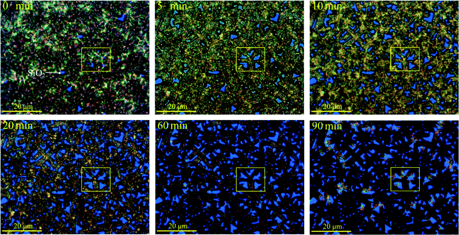 | ||
| Fig. 4 Spray coated film probed in situ during the anneal at 110 °C under an optical microscope. The measurements were performed with a 32× magnification lens. | ||
Conclusions
We have presented an investigation of the evolution of texture during the thermal annealing of mixed lead halide perovskites using in situ 2D synchrotron GI-WAXS. For this class of polycrystalline materials, the use of a 10 keV wide-focussed X-ray beam allows a large number of grains to be probed simultaneously. To explore this complex phenomenon, we have presented an efficient way to classify the behaviour of many hundreds of tracks using a self-organising map. The statistical picture that emerges indicates that individual precursor and perovskite grains undergo rotation and lattice compression or expansion during annealing; a process likely driven by strain within the film as a result of the chemical conversion process. Characterising and controlling the dynamics of crystal formation is essential in the development of perovskite films having improved flatness and order, as such characteristics are generally associated with improved device efficiency. The techniques demonstrated here can be employed in the study of a large range of other polycrystalline materials having similar crystallisation dynamics.Experimental section
Materials
Si/SiO2 substrates were purchased from Ossila Ltd (UK), cleaned by sonication in isopropyl alcohol and deionized water, and dried with compressed nitrogen before use. Methylammonium iodide (MAI) powder was synthetized as per our previous works.8,21 Lead II chloride (PbCl2, 98% purity) was purchased from Sigma Aldrich (268690, Aldrich). Precursor solutions of MAI and PbCl2 (3:1 molar ratio) were dissolved in sequence into dimethylformamide (DMF) with a concentration of 664 mg ml−1, heated at 70 °C overnight to facilitate dissolution of solid material, cooled to room temperature, and then filtered through a 0.45 mm PTFE filter before use.8,21
Experimental setup
Technical details on the XMaS (ESRF) beamline setup are reported on the beamline website http://www.xmas.ac.uk. The radiation coming from a bending magnet (critical energy Ec = 9.8 keV) was monochromatised using a fixed-exit, water-cooled, double crystal Si(111) monochromator, placed at 25 m from the source. A Rh-coated toroidal mirror was used to focus the monochromatic beam horizontally and vertically. The beam flux was ∼5 × 10¹⁰ photons s−1 at the sample position. The original beam spot size without slits was 500 (horizontal) × 400 (vertical) μm2 at the sample position. We employed a set of slits immediately before the sample to have a better defined footprint in the vertical direction. The final beam spot size with slits was 500 (horizontal) × 100 (vertical) μm2. Note that the horizontal beam profile had a Gaussian shape with a FWHM of 500 μm. Note that the vertical beam profile had a top hat shape of width 100 μm as it was vertically clipped by the slits. We thus calculate a beam footprint of 500 (horizontal) × 1910 (vertical) μm2. A MAR 165 CDD detector with 2048 × 2048 pixel active area and 80 μm pixel size was placed at 203 mm from the sample, detecting 10 keV monochromatic X-rays. The distance between the sample and the detector was calibrated as in previous reports by tracking the direct beam position at different azimuth (2θh) and elevation detector (2θv) coordinates.21–23 A custom-made annealing chamber (see Fig. 5) was manufactured via 3D printing. We used an EOS P110 3D printer (EOS GmbH, Germany) for the nylon plastic parts, and an EOS M270 3D-printer for the aluminium parts. Both printers build parts layer by layer, using a bed of powder that was melted with a laser. The P110 heated the build chamber to within 10 °C of the plastic's melting temperature, and provided the rest of the energy to fuse the layers with a 30 W CO2 laser. The M270 uses a 200 W fiber laser to directly sinter the aluminium powder. The chamber contained a heating stage that incorporated a cooling spiral that was connected to a chiller and a cartridge heater that was controlled via an Eurotherm temperature controller. The Si/SiO2 substrate was kept in place on the heating stage through a small cavity connected to a vacuum pump. The annealing chamber was connected to a metal pedestal fixed on a cryostat mount (Huber 5012 mount). The cryostat mount fitted into the Huber 410 phi circle on the 11-axis Huber diffractometer. The spray coater employed for the preparation of the in situ samples was made of a 3D metal printed cavity with 2D array of 500 μm holes and was placed 5 cm from the heating stage inside the annealing chamber. For the deposition phase, the heating stage was set to 60 °C two hours before the actual deposition to avoid any thermal expansion during the measurements. The perovskite precursor solution was introduced in the spray coater metal cavity. Introducing a sample in the annealing chamber, sealing the chamber, flushing helium and starting the acquisition of diffraction images took ∼1 min. The perovskite solution was sprayed on the sample by flushing nitrogen through the metal cavity from a manual valve located at the synchrotron beamline control cabin. After deposition, the sample was kept on the hotplate for ∼10 min and stored in ambient conditions. For the annealing phase, the heating stage was set to 110 °C three hours before the actual annealing to avoid any thermal expansion during the measurements. The deposited spray coated film had a thickness of ∼1100 nm.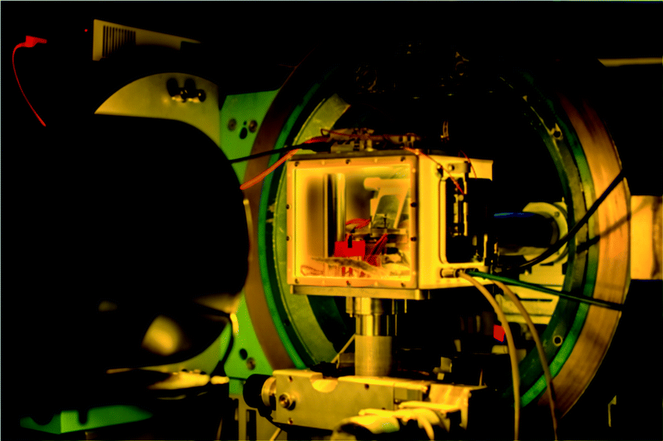 | ||
| Fig. 5 Custom-made annealing chamber used fort GI-WAXS measurements at the XMaS beamline (ESRF). See also ESI† and ref. 23. | ||
Image processing
Data processing was performed using a GI-XRD MATLAB software.24 The 390 images collected during the deposition and the annealing phases were remapped into scattering vector coordinates, as detailed in ref. 23. The scattering vector is defined as q = kf − ki = [qxqyqz], where ki is the incident wave vector and kf is scattered wave vector. Here, the scattering vector q is referred to the Euclidean norm of q. Images are represented in reduced scattering vector rectangular coordinates: qz and . We also refer to scattering vector polar coordinates: azimuth χ = π/2 − atan(qz/qxy) in degrees and distance
 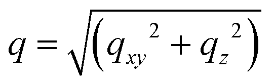 , which corresponds to the wavevector 2π/λ, where λ is the beam wavelength. Intensity in the diffraction patterns shown in Fig. 1 is normalized between 0 and 1. Azimuthally integrated line profiles are generated as shown in ref. 24 between χ = 15.5° and χ = 88.5°, thus excluding the missing image cake below χ = 15.5° due to the pixel to scattering vector coordinates conversion. Line profiles are displayed using a linear scale. The weak PbI2 peak due to perovskite degradation and near q = 0.9 Å–1 is only visible on a logarithmic scale.
Diffraction spot tracking
A spot-tracking program was written in MATLAB and integrated in the GI-XRD software. An original remapped image was treated with background removal and top hat filtering to enhance the local diffraction spots and facilitate 2D peak detection. An image processing MATLAB algorithm commonly used for tracking moving colloidal particles (J. Crocker's track.pro routine) was modified to work with the moving diffraction spots.25 A matrix containing the (x,y) coordinates of the detected spots in each image and time (or equivalently image) index was fed into the tracking routine. As an example, in the 60 images of the deposition phase, the number of detected spots was 155420. However only tracks lasting more than 11 images (i.e. ∼3 min) and with a maximum displacement higher than 10 pixels were selected. Large diffraction spots with displacement above 4 pixels were not considered. Diffraction spots with excessive overlap to other diffraction spots and stationary spots were also not included. For each track and each image corresponding to the track, we generated a region of interest (ROI) having the diffraction spot coordinates at its centre. The diffraction spot was fitted with a 2D Gaussian, which was then used as a shape-preserving filter to generate a new ROI, where only the diffraction spot is visible. The image was then converted to a black and white ROI and information on the diffraction spot shape extracted, such as area, eccentricity, orientation, etc. Videos of each single track were also generated (see ESI†). Videos were checked by hand and false tracks removed from the dataset. Under these conditions the number of tracks detected in the deposition image set and the annealing set was 32 and 601 respectively. We automatically analysed 980 and 32892 ROIs for the deposition and the annealing set respectively.
Track clustering
During the deposition phase we did not observe any ring from the perovskite structure. However, during the anneal we observed reflections from both the precursor and perovskite polycrystal. The tracks detected in the annealing phase have thus been classified into precursor and perovskite tracks. Tracks within the perovskite rings that lasted until 80 min were classified as perovskite tracks. The remaining tracks were classified as precursor tracks. As discussed in the text, a further classification was performed of the precursor and perovskite tracks using a self-organizing map (SOM) in MATLAB.20 A SOM is an artificial neural network made of a competitive layer that can classify a dataset of vectors into a number of classes equal to the number of neurons in the layer. A single input in a SOM is an N-dimensional vector, but cannot be an N × M matrix. In our case a generic i-th track was represented by a Ni × 3 matrix with Δqi = [Δq1iΔq2i⋯ΔqNi]T, Δχi = [Δχ1iΔχ2i⋯ΔχNi]T, and time ti = [t1it2i⋯tNi]T as the columns. Therefore, the input dimension had to be reduced from 3D to 1D, while preserving the track information. By resampling Δqi and Δχi so that the 601 tracks had the same N length, we represented the i-th track by an N × 2 matrix with Δq′i = [Δq′1iΔq′2i⋯Δq′N]T and Δχ′i = [Δχ′1iΔχ′2i⋯Δχ′N]T as the columns. A further dimensional reduction for the i-th track was obtained by constructing a 2N vector that contained alternating distance and azimuth displacement elements, i.e. [Δχ′1iΔq′1iΔχ′2iΔq′2i⋯Δχ′NΔq′N]T. This dimensional reduction preserved the information on the track behaviour and was used to train the SOMs. The networks were trained using an unsupervised learning algorithm to produce a 2D topology allowing the layer to form a two-dimensional representation of the dataset topology. The SOM trained for the 529 precursor tracks dataset is illustrated in Fig. S11 (ESI†). The network consisted of a layer of 4 × 4 = 16 neurons or clusters and was trained 5 times (1000 epochs) with the default algorithm (trainbu). When a track vector was inputted to the SOM, the SOM returned one of the 16 clusters. Tracks were further manually classified based on the Cartesian quadrant where they were located. Intuitively we could have used a simpler 2 × 2 SOM, however the clustering strategy reported here was more effective. In the case of the 72 perovskite tracks, the trained 2 × 2 SOM performed effectively, and the use of larger SOMs did not result in any improved performance (see Fig. S12, ESI†).Acknowledgements
This work was funded by the UK Engineering and Physical Sciences Research Council via grants EP/M025020/1 ‘High resolution mapping of performance and degradation mechanisms in printable photovoltaic devices’, EP/J017361/1 (Supersolar Solar Energy Hub) and the E-Futures Doctoral Training Centre in Interdisciplinary Energy Research EP/G037477/1. This work was partially funded by ‘The President of the UAE's Distinguished Student Scholarship Program (DSS), granted by the Ministry of Presidential Affairs, UAE’ (M.A. PhD scholarship). XMaS is a mid-range facility supported by the Engineering and Physical Sciences Research Council (EPSRC). We are grateful to all the XMaS beamline team staff for their support. We thank Robert Masters for performing the SEM scans.References
- D. B. Mitzi, C. A. Feild, W. T. A. Harrison and A. M. Guloy, Nature, 1994, 369, 467–469 CrossRef CAS.
- A. Kojima, K. Teshima, Y. Shirai and T. Miyasaka, J. Am. Chem. Soc., 2009, 131, 6050–6051 CrossRef CAS PubMed.
- P. Gao, M. Gratzel and M. K. Nazeeruddin, Energy Environ. Sci., 2014, 7, 2448–2463 CAS.
- M. A. Green, K. Emery, Y. Hishikawa, W. Warta and E. D. Dunlop, Prog. Photovoltaics, 2015, 23, 805–812 Search PubMed.
- M. M. Lee, J. l. Teuscher, T. Miyasaka, T. N. Murakami and H. J. Snaith, Science, 2012, 338, 643–647 CrossRef CAS PubMed.
- Z.-K. Tan, R. S. Moghaddam, M. L. Lai, P. Docampo, R. Higler, F. Deschler, M. Price, A. Sadhanala, L. M. Pazos, D. Credgington, F. Hanusch, T. Bein, H. J. Snaith and R. H. Friend, Nat. Nanotechnol., 2014, 9, 687–692 CrossRef CAS PubMed.
- F. Deschler, M. Price, S. Pathak, L. E. Klintberg, D.-D. Jarausch, R. Higler, S. Hüttner, T. Leijtens, S. D. Stranks, H. J. Snaith, M. Atatüre, R. T. Phillips and R. H. Friend, J. Phys. Chem. Lett., 2014, 5, 1421–1426 CrossRef CAS PubMed.
- A. T. Barrows, A. J. Pearson, C. K. Kwak, A. D. F. Dunbar, A. R. Buckley and D. G. Lidzey, Energy Environ. Sci., 2014, 7, 2944–2950 CAS.
- A. Dualeh, N. Tétreault, T. Moehl, P. Gao, M. K. Nazeeruddin and M. Grätzel, Adv. Funct. Mater., 2014, 24, 3250–3258 CrossRef CAS.
- D. T. Moore, H. Sai, K. W. Tan, D.-M. Smilgies, W. Zhang, H. J. Snaith, U. Wiesner and L. A. Estroff, J. Am. Chem. Soc., 2015, 137, 2350–2358 CrossRef CAS PubMed.
- Z. Xiao, Q. Dong, C. Bi, Y. Shao, Y. Yuan and J. Huang, Adv. Mater., 2014, 26, 6503–6509 CrossRef CAS PubMed.
- B. S. Tosun and H. W. Hillhouse, J. Phys. Chem. Lett., 2015, 6, 2503–2508 CrossRef CAS PubMed.
- D. W. de Quilettes, S. M. Vorpahl, S. D. Stranks, H. Nagaoka, G. E. Eperon, M. E. Ziffer, H. J. Snaith and D. S. Ginger, Science, 2015, 348, 683–686 CrossRef CAS PubMed.
- A. Sharenko and M. F. Toney, J. Am. Chem. Soc., 2016, 138, 463–470 CrossRef CAS PubMed.
- L. Margulies, G. Winther and H. F. Poulsen, Science, 2001, 291, 2392–2394 CrossRef CAS PubMed.
- Z. Huang, M. Bartels, R. Xu, M. Osterhoff, S. Kalbfleisch, M. Sprung, A. Suzuki, Y. Takahashi, T. N. Blanton, T. Salditt and J. Miao, Nat. Mater., 2015, 14, 691–695 CrossRef CAS PubMed.
- R. Christian, B. Manfred and D. Richard, IOP Conf. Ser.: Mater. Sci. Eng., 2010, 14, 012013 CrossRef.
- H. F. Poulsen, S. F. Nielsen, E. M. Lauridsen, S. Schmidt, R. M. Suter, U. Lienert, L. Margulies, T. Lorentzen and D. Juul Jensen, J. Appl. Crystallogr., 2001, 34, 751–756 CrossRef CAS.
- H. Poulsen, Appl. Phys. A: Mater. Sci. Process., 2002, 74, 1673–1675 CrossRef.
- T. Kohonen, Biol Cybern, 1982, 43, 59–69 CrossRef.
- A. T. Barrows, S. Lilliu, A. J. Pearson, D. Babonneau, A. D. F. Dunbar and D. G. Lidzey, Adv. Funct. Mater., 2016 DOI:10.1002/adfm.201601309.
- S. Lilliu, M. Alsari, O. Bikondoa, J. E. Macdonald and M. S. Dahlem, Sci. Rep., 2014, 5, 1 Search PubMed.
- S. Lilliu and T. Dane, arXiv:1511.06224 [cond-mat.soft], 2015, vol. 1, p. 1.
- S. Lilliu, T. Agostinelli, E. Pires, M. Hampton, J. Nelson and J. E. Macdonald, Macromolecules, 2011, 44, 2725–2734 CrossRef CAS.
- J. C. Crocker and D. G. Grier, J. Colloid Interface Sci., 1996, 179, 298–310 CrossRef CAS.
Footnote |
| † Electronic supplementary information (ESI) available: Links to Videos 1–22; GI-WAXS and solar cell measurements on spin coated samples; SEM measurements on spray and spin coated samples; Fig. S1–S15; Table S1. See DOI: 10.1039/c6ce00965d |
| This journal is © The Royal Society of Chemistry 2016 |