
 Open Access Article
 This Open Access Article is licensed under a
 Creative Commons Attribution 3.0 Unported Licence
Droplet-induced dot, dot-in-hole, and hole structures in GaGe thin films grown by MOCVD on GaAs substrates†
Hongfei
Liu
*,
Yunjiang
Jin
and
Chengyuan
Yang
Institute of Materials Research and Engineering (IMRE), A*STAR (Agency for Science, Technology and Research), 2 Fusionopolis Way, Singapore 138634, Singapore. E-mail: liuhf@imre.a-star.edu.sg
First published on 5th May 2016
Abstract
We report observations and origins of Ga-rich GaGe droplets and the localized etching of Ge-rich GaGe thin films grown on GaAs (100) substrates by metalorganic chemical vapor deposition. Micron and sub-micron dots, dot-in-holes, and holes have been fabricated by controlling the partial pressures of the Ga and Ge precursors as well as the substrate temperatures. The dot-in-hole features can also be converted to empty holes via post-growth sonication in hot deionized water due to the low melting point of the Ga-rich dots. Enhanced Raman scattering (ERS) of the Ge–Ge lattice vibrational mode has been observed at the wall of the concentric dot-in-hole structures as well as in the empty holes. To interpret the ERS mechanism, we have carried out finite-difference time-domain (FDTD) simulations, which reveal an enhanced electrical field for the obtained structures as a result of interference between the incident and reflected waves at the surface of the thin films that, in turn, results in the observed ERS. These findings greatly enrich the conventional droplet epitaxy and etching techniques and widen their applications.
1. Introduction
The epitaxial growth of III–V arsenide/antimonide quantum dots (QDs) via converting pre-deposited metal droplets, e.g., Ga droplets on a ZnSe substrate,1 under arsenic and/or antimony flux, so-called droplet epitaxy (DEPI), was discovered two decades ago.1,2 This method, being different from the conventional Stranski–Krastanov growth mechanism where a lattice mismatch between the growing materials and the template/substrate is generally required and the grown structures are basically limited to QDs,3,4 provides additional freedom for fabricating quantum structures, e.g., quantum rings and concentric multiple quantum rings.5–10 The metal droplets, when heated without the presence of group V reaction species, induce backward melting of the template, which, followed by thermal evaporation of the remaining metal atoms of the droplets, leads to the formation of holes in the template. This process, so-called droplet etching (DETC) or drilling, has emerged and has been extensively studied in the past ten years.11–16 The combination of DEPI and DETC has created a facile nanotechnology for fabricating various functional structures towards practical applications in optical and optoelectronic devices.17–21A careful literature survey shows that although DEPI and DETC studies are dominated by molecular beam epitaxy (MBE), explorations of DEPI by using metalorganic chemical vapor deposition (MOCVD) have started soon after MBE;22,23 nevertheless, these studies are generally limited to III–V materials.2,5–22 In comparison, DEPI and DETC studies on hetero-substrates are much fewer in the literature although heterogeneous material integrations,1,23e.g., III–V-on-Si/Ge, are highly desired for electrical and optoelectronic applications such as bipolar transistors,24 tandem solar cells,25–27 broadband photodetectors,28etc.23,29–32 Recent developments in surface plasmonics and metamaterials have seen many new applications of combining metallic nanoparticles and semiconductors in various configurations to enhance light absorption and/or scattering.33–36 For this purpose, both unintentional surface V-shaped defects (i.e., V-pits) and intentionally patterned V-shaped holes in semiconductors have been employed for locating metal dots to enhance their surrounding optical near-field so as to couple into the active regions embedded in the semiconductor structures.35,37
Here, we demonstrate a novel mechanism for creating Ga droplets on GaGe thin films epitaxially grown by MOCVD on lattice-matched GaAs (100) substrates; by tuning the Ga composition (i.e., via adjusting the flow rate ratio of Ga/Ge precursors) and the growth temperature, dot, dot-in-hole, and hole structures are well created in the GaGe thin films due to the finite solubility of Ga atoms in the crystalline Ge matrix and vice versa.38–41 Enhanced Raman scattering (ERS) of the Ge–Ge lattice vibrational mode has been observed at the ring-like walls around the droplet-structured areas as well as in the holes. The mechanism for the observed droplet-induced structures is dedicatedly discussed based on growth kinetics. Three-dimensional finite-difference time-domain (FDTD) simulations have also been carried out to interpret the ERS mechanism. The grown structures are of great consequence in studies and application of the electrical and optoelectronic properties of GaGe thin films.
2. Experimental procedure
A horizontal low-pressure MOCVD reactor (Aixtron 200/4) was employed for the epitaxial growth of GaGe-on-GaAs and the general growth procedures can be found in our earlier publications.42,43 Trimethylgallium (TMGa), tertiary-butylarsine (TBAs), and germane (GeH4) were used as the Ga, Ge, and As precursors, respectively. Highly purified H2, through a heated palladium cell, was used as the carrier gas and the chamber pressure was set at 10 kPa during growth. For the GaGe thin film growth, the flow rates of the Ga and Ge precursors were set at 5.6 × 10⁻⁶ and 9.2 × 10⁻⁴ mol min−1, respectively. The GaAs (100) substrates were cleaned for 10 seconds in a diluted HF solution (10%), followed by a sequence of three 5 minute ultrasonication processes in acetone, isopropenyl acetylene, and deionized water.Before starting the GaGe growth, the GaAs substrate was heated to 600 °C and kept at this temperature for 5 minutes under TBAs flow, so that potential residual oxides can be completely removed. After heat treatment, a GaAs buffer layer about 100 nm thick is usually grown by feeding TMGa to obtain an atomically smooth surface. At the end of the buffer growth, feeding of TMGa was stopped and the substrate temperature was ramped to the target growth temperature TG (in the range of 550 to 630 °C). The growth of GaGe was started once TG was reached by stopping the supply of TBAs and feeding TMGa and GeH4. The nominal thickness of the GaGe thin films, controlled by the growth time that depends on TG, is 1.0 μm in this study.
The grown GaGe thin films were characterized by using various techniques including atomic force microscopy (AFM), scanning electron microscopy (SEM), energy-dispersive X-ray spectroscopy (EDX), high-resolution X-ray diffraction (HRXRD), room-temperature Raman scattering, Hall-effect measurement, etc. For the Raman scattering, a confocal micro-Raman system (Witec alpha 300) in a backscattering configuration was used, which has the advantage of being able to carry out high-resolution mappings. The 532 nm line of an argon-ion laser was used as the excitation source, for which the beam size on the sample surface can be focused to ∼0.9 μm diameter when a high-magnification objective lens is used (i.e., ×100).
3. Results and discussion
Fig. 1(a)–(c) present the AFM images recorded in 10 × 10 μm2 from GaGe thin films (∼1.0 μm thick) grown at TG = 550, 600, and 630 °C, respectively. Fig. 1(d) plots the densities of the surficial features as a function of the growth temperatures. The densities were accounted for by averaging several samples grown under the same conditions and by using various microscopic techniques such as SEM and optical photography depending on the densities (see, e.g., Fig. 3 and S1 in the ESI†). Dots, dot-in-holes, and holes are clearly seen in Fig. 1(a)–(c), respectively. The dots, either on the film surface or concentric in the holes, exhibit round boundaries at the bases (i.e., the triple line of droplets) while the holes have a square opening on the surface, surrounded by walls higher than the film surface at the areas away from the features. Fig. 2 shows more details of the surface structures. Shown in Fig. 2(a) are the line traces across the structures shown in Fig. 2(b)–(d). One sees that when TG is increased from 550 to 630 °C while keeping the other growth conditions constant, the observed structures gradually develop from dots through dot-in-holes to empty holes. Fig. 2(e)–(g) show that at a certain growth temperature (i.e., TG = 600 °C), an increase in the flow rate of TMGa from 5.6 × 10⁻⁶ to 8.4 × 10⁻⁶ mol min−1 while keeping that of GeH4 unchanged does not change the geometry of the dot-in-hole structures but increases their sizes. | ||
| Fig. 1 AFM images recorded in a tapping mode from GaGe thin films grown by MOCVD on GaAs (100) substrates at 550 °C (a), 600 °C (b), and 630 °C (c). The Arrhenius plot in (d) displays the feature densities on the surface as a function of growth temperatures, which yields a characteristic energy of 2.85 eV. | ||
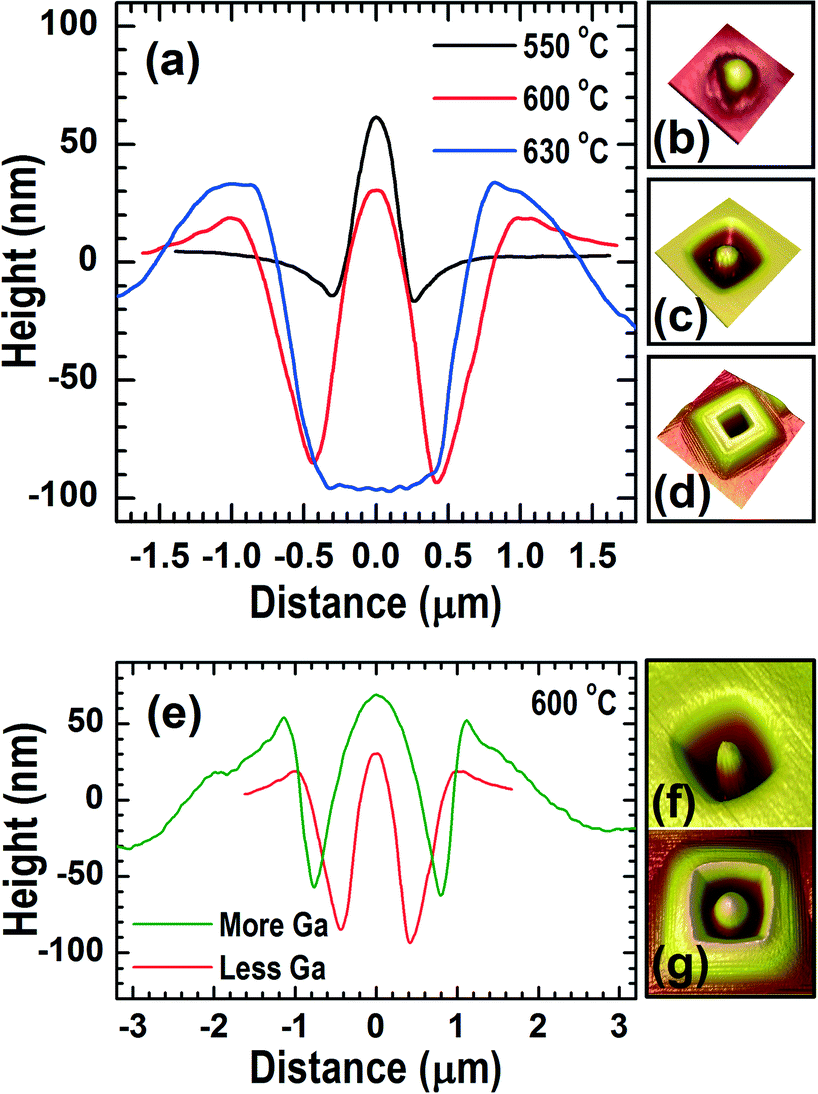 | ||
| Fig. 2 Height profiles (a) across the droplet-induced dots (grown at 550 °C), dot-in-holes (grown at 600 °C), and holes (grown at 630 °C) on the GaGe thin films. (b)–(d) are the AFM images for typical dot, dot-in-hole, and hole features, respectively. (e)–(g) show that the dot-in-hole structure is also tunable by controlling the partial pressure of the Ga precursor (TMGa). | ||
A careful observation of the AFM images reveals that the opening of the holes is aligned with their edges parallel to the [110] and [1−10] axes of the GaAs (100) substrate, indicating that the GaGe thin films are epitaxially grown on the substrate. The epitaxial growth of the GaGe thin films has further been confirmed by HRXRD and Raman scattering characterization (see ESI† Fig. S2). The small full-width at half-maximum (FWHM) values (≤18 arcsec) of the HRXRD Ge (004) rocking curves as well as the clear fringes of the θ–2θ scans are indicative of the high crystal quality of the GaGe thin films and a smooth interface of GaGe-on-GaAs. The downward shift (i.e., softening) of the Ge–Ge lattice vibrational mode to ∼291.2 cm−1 from that of bulk Ge at ∼298.2 cm−1 is mainly caused by an alloying of Ga atoms, which is commonly observed in semiconductor alloys.44–46 It should be noted that the lattice strain built in the GaGe thin films is in the range of εxx = −850 ppm as measured by reciprocal space mapping (see ESI† Fig. S3). This amount of strain would cause an upward shift (i.e., mode hardening) of less than 0.5 cm−1 for the Ge–Ge mode.44,45
The Arrhenius plot in Fig. 1(d) yields a density-related characteristic energy of EN = 2.85 eV, which is much larger than those of Ga droplets deposited on Si and GaAs substrates—in the range of 0.50–0.76 eV—but quite close to that of In droplets deposited on a GaAs substrate (2.21 eV).15,37 A root-mean-square roughness analysis at the areas away from the features reveals a surface roughness of 0.7–2.3 nm for the as-grown GaGe thin films while EDX analyses at these planar regions reveal that the Ga composition monotonically increases with growth temperature, which is 5.2, 5.6, and 5.8 at% for the GaGe thin films grown at TG = 550, 600, and 630 °C, respectively.43 An Arrhenius plot of the Ga compositions (see ESI† Fig. S4) yields an activation energy of 87 meV for Ga atoms to incorporate into the GaGe thin films. This value is much smaller than the density-related characteristic energy (i.e., EN = 2.85 eV) obtained from the Arrhenius plot in Fig. 1(d); it is also much smaller than the activation energy of evaporation from elemental Ga (2.9 eV).47 These comparisons indicate the presence of liquid Ga and/or Ga-rich GaGe liquid on the growing surface and the alloying process of GaGe thus occurs directly from the surficial liquid rather than controlled by surface diffusion during growth.47,48 On the other hand, the desorption rate of surficial Ga is faster at higher TG, i.e., with an activation energy of 2.9 eV.47 In this regard, the increased alloy compositions of Ga in the grown GaGe thin films must originate from a more significantly increased pyrolytic decomposition of TMGa than that of GeH4 at higher temperatures, which is consistent with the increased growth rates at higher temperatures in the studied temperature range.42,43,49
The formation of liquid Ga on the growing surface of GaGe, completely different from those of pure metal deposition in conventional DEPI and DETC techniques, is most likely due to atomic surface segregation and phase separation because of the low solubility of Ga in Ge and the finite solubility of Ge and Ga.38–41 Since the maximum solubility of Ga atoms in Ge is about 1.1 at%,40 a TMGa/GeH4 precursor ratio that produces more than 1.1 at% Ga on the growing surface could lead to a phase separation between Ga-rich and Ge-rich GaGe. The former is in liquid while the latter is in solid phase at the studied growth temperatures (550–630 °C). The liquid phase Ga-rich GaGe tends to segregate onto the growing surface while the Ge-rich GaGe contributes to the growth of the solid thin films.47,48,50 As a consequence, Ga-rich droplets stem from clustering and coalescence of the accumulating Ga-rich GaGe on the growing surface of the Ge-rich GaGe thin films.51,52 It is worth noting that the Ga compositions of 5.2–5.8 at% as probed by EDX in the epitaxial GaGe thin films are much larger than the solid solubility of Ga in Ge (1.1 at%).40 This is not surprising since the solid solubility was determined in a thermodynamic equilibrium state of the alloy while the thin films studied here were deposited in a metastable situation, which is far from the thermal equilibrium state. In light of this, the solubility characteristics of Ga in Ge, depending on the thin film processing techniques, could be higher in thin films than those in bulk.53–55 For example, a single phase homogeneous amorphous GaGe thin film with a Ga composition of 5 at% has been prepared by Nath et al.53 employing physical vapor deposition.
We have mentioned above that in comparison to the migration of Ga adatoms on Si substrates, the density-related characteristic energy of Ga-rich droplets on the surface of Ge-rich GaGe thin films is relative larger. This comparison clues us in that a pinning–depinning mechanism,51,52,56 kinetically controlled by the incorporation and desorption reaction species at the liquid/solid interfaces, dominates the surficial migration of the Ga-rich droplets. In this regard, the growth temperature also plays an important role in the Ga-rich droplet migration via tuning the desorption rate of atoms at the liquid/solid interface during film growth, which is similar to droplet-induced drilling/etching in the conventional DETC technique.11–16Fig. 3(a) and (b) present the top-view SEM images recorded from the GaGe thin film samples grown at TG = 550 and 600 °C, respectively. The migration and coalescence traces of the surface droplets are clearly seen on the surface of the GaGe thin film grown at TG = 550 °C, some of which have been indicated by the arrows in Fig. 3(a) while many others have been smeared or covered due to the steady-state growth of Ge-rich GaGe. Elemental analyses by EDX using linear scans across the dot and dot-in-hole structures as indicated in Fig. 3(a) and (b) are presented in Fig. 3(d) and (e), respectively. Likewise, a typical SEM image and elemental distributions recorded from the GaGe thin film grown at 600 °C but followed by an additional sonication process in deionized (DI) water at 80 °C for 30 minutes are presented in Fig. 3(c) and (f), respectively.
 | ||
| Fig. 3 Top-view SEM images recorded from the GaGe thin films grown at 550 °C (a), 600 °C (b), and 600 °C followed by an additional ultrasonication process in hot (80 °C) deionized water (c). (d)–(f) are the elemental distributions of Ga and Ge across the surface features collected by using an EDX spectrometer installed in the SEM chamber. Please note the droplet coalescence traces indicated by the arrows and the removal of the Ga-rich dots from the dot-in-hole structures by the ultrasonication process. | ||
The SEM images and elemental analyses in Fig. 3 provide clear-cut evidence that the dots are Ga-rich and the flat films are Ge-rich GaGe. The Ga-rich dots have a low melting point, at least lower than 80 °C, and are thus feasibly removed by post-growth sonication in hot water [see the SEM comparisons in Fig. 3(b) and (c) and the optical microscopic comparisons in ESI† Fig. S1(a) and (b) for details]. These results, together with the feature evolution as a function of growth temperatures observed by AFM, suggest that (i) at the initial growth stage, the migration velocity of the Ga-rich droplets increases with growth temperature, (ii) as the growth continues at a certain temperature, the droplets grow in size (partly via droplet coalescence) and tend to lose their mobility, and (iii) the onset of decomposition of Ge-rich GaGe occurs at the liquid/solid interface of the droplets and once they stopped running on the surface, the decomposition rate increases with growth temperature at this stage. Newly generated droplets at this stage are feasibly captured by the bigger ones before they are grown bigger because of their increased mobility at higher temperatures. The decomposition of Ge-rich GaGe at the droplet boundaries dissolves Ge into the droplet while the Ga atoms tend to be wicked away from the droplet by capillary actions,57 which further react with absorbed Ge species from the vapor to form the ring-like Ge-rich GaGe walls around the droplets (see Fig. 2). At higher growth temperatures, e.g., ≥600 °C, the increased decomposition at the base boundaries of the droplets and the wicking out of Ga atoms tend to lower the base of the droplets and give rise to the dot-in-hole structures [see Fig. 1(b), 2(c), (f), (g) and 3(b)]. This progress, together with the ever increasing desorption rates of Ga atoms from the Ga-rich droplets with temperature under the chosen growth conditions, eventually leads to complete evaporation of the droplets from the holes [see Fig. 1(c), 2(a) and (d)].
Micro-Raman mappings have further been carried out for the GaGe thin films addressing the effects of the Ga-rich dot structures. The mappings are targeted at the Ge–Ge lattice vibrational mode at about 290 cm−1; the typical Raman spectra are shown in ESI† Fig. S2(b). Presented in Fig. 4(a) and (c) are the peak intensity mappings for the GaGe thin films grown at 550 and 600 °C, respectively. For comparison, the peak intensity mapping of the film grown at 600 °C but followed by an additional ultrasonication process in hot DI water is presented in Fig. 4(e). Likewise, their frequency mappings are shown in Fig. 4(b), (d), and (f). The scale bars are 4.0 μm. The Raman mappings in Fig. 4(a) and (c) clearly show that the presence of the Ga-rich dots significantly weakened the Raman scattering intensities of the Ge–Ge mode for both the dot and the dot-in-hole structures. The Raman signals from the base boundaries of the dot structures are also weakened as compared with those from the flat film areas [see Fig. 4(a)]. The weakening in Raman scattering at the dot areas can be simply due to blockage of the laser beam by the Ga-rich dots from the Ge-rich GaGe underneath. The still detectable Raman signals from the dot areas (see ESI† Fig. S5) could be either due to incomplete blockage of the laser beam, because the beam size of ∼900 nm is quite close to the size of the dots, or due to precipitates and/or nucleation of Ge-rich GaGe at the base boundaries of the Ga-rich dots because of the wicked Ga. The latter case is quite possible since segregation of Ge atoms from Ga droplets to recrystallize at the base boundary (i.e., the triple line) of the Ga droplets has already been observed in earlier studies.58
 | ||
| Fig. 4 Micro-Raman mappings collected from the GaGe thin films grown at 550 °C (a and b), 600 °C (c and d), and 600 °C followed by an additional ultrasonication process in hot deionized water (e and f). The scale bars are 4 μm and the mappings on the left (right) column are the peak intensity (wavenumber) distributions of the Ge–Ge lattice vibrational mode; for the spectral details, please see Fig. S2(b) and S4 provided in the ESI.† | ||
In contrast to Raman scattering weakening at the dot areas, the Raman signals from the ring-like walls of the dot-in-hole structures are apparently enhanced as compared with those from the flat film areas [see Fig. 4(c)]. The most interesting observation was made after the removal of the Ga-rich dots from the holes, where the Raman signals are remarkably enhanced [see Fig. 4(e)]. The frequency mapping in Fig. 4(b) does not show any apparent contrast between the dot and flat areas; however, frequency contrasts are clearly seen in Fig. 4(d) and (f). A combination of Fig. 4(c)–(f) reveals that those areas with enhanced Raman intensity exhibit lower Raman frequencies (i.e., mode softening) and vice versa. Comparisons of typical Raman spectra from the dot/hole, boundary/wall, and flat areas are shown in ESI† Fig. S5. The correlation between the ERS and the mode softening clearly indicates that the Raman scattering enhancement at the walls of the dot-in-hole structures and the center of the empty holes is associated with both the GaGe materials and the local structures. To understand the ERS mechanism of the dot-in-hole and the hole structures, we have further carried out FDTD simulations.
For the FDTD simulations, because the optical parameters of Ge-rich and Ga-rich GaGe are not available, the refractive indices of Ge (4.90 + i2.40) and Ga (1.27 + i6.54) at the wavelength of 532 nm were, instead, used for the film and the dot, respectively.59,60 A light source with a normal incident plane wave at the wavelength of 532 nm, i.e., the same as that for the Raman scattering measurements, was set in front of the structures [see the schematic diagrams in ESI† Fig. S6(a) and (b)]. The magnitude of the plane wave was set to unity and the polarization was set in the horizontal direction, i.e., the X-axis. Fig. 5(a) and (b) show the magnitude distributions of the electrical field on the surface of the thin films with and without the metallic dot. Plotted in Fig. 5(c) and (d) are the field magnitudes on the surface across the dot-in-hole and the hole structures. The electrical field distributions clearly show a field enhancement at the wall of the dot-in-hole structure as well as in the hole without the Ga dot. The enhancement is due to the interference between the incident and reflected waves on the Ge surface, which can be seen from the cross-sectional field distributions shown in the ESI† [see Fig. S6(c) and (d)]. The constructive interference leads to a strong electrical field at the walls and inside the holes, which enhances the Raman scattering therein.
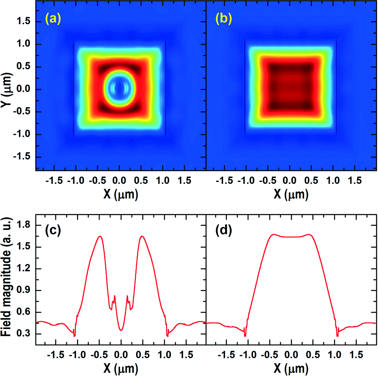 | ||
| Fig. 5 Distributions of the electrical field magnitude on the surface of a germanium hole structure with (a) and without (b) a gallium dot located at the hole center calculated by using a three-dimensional finite-difference time-domain (FDTD) simulation. (c) and (d) show the corresponding field magnitudes on the surface across the dot-in-hole and hole structures. The configurations and setup for the simulations are shown in ESI† Fig. S5. | ||
Four-probe van der Waals Hall-effect measurement at room temperature revealed a resistivity of 7.35 × 10⁻⁴ Ω cm for the as-grown GaGe thin film; likewise, the carrier (p-type) density and mobility are 2.82 × 1020 cm−3 and 30.1 cm2 V−1 s−1, respectively. From the p-type doping point of view, the Hall mobility of 30.1 cm2 V−1 s−1 at the doping level of 2.82 × 1020 cm−3 agrees well with those of p-type Ge at room temperature (i.e., μH = 35–105 Ω cm for N = 1020–1021 cm−3) reported by Golikova et al.;61 meanwhile, the resistivity of 7.35 × 10⁻⁴ Ω cm of our GaGe thin film is about two times larger than that derived from ρ = N−α/B with B = 1.11 × 10⁻⁹ Ω−1 cm−1 and α = 0.609 in the range of 1019 ≤ N ≤ 1020 reported by Cuttriss for p-type Ge at room temperature.62 These results indicate that the GaGe thin films still exhibit the typical doping behavior of p-type Ge at very high doping levels. On the other hand, the sheet resistance of the as-grown GaGe thin films is about 7–20 Ω sq−1, which is in the range of conductors such as ITO and much smaller than those of Ge reported in the literature.63 A comparison between the carrier concentration and the Ga composition (5.2 at%) of the GaGe thin film shows that about 0.64% of Ge lattice sites were occupied by Ga atoms that gave rise to the p-type doping; the remaining Ga atoms thus most likely occupy the interstitial and/or splitting complex positions in the GaGe thin film. It has to be noted that the presence of the Ga-rich dots on the film surface does not contribute any detectable electrical conductivity as verified by the unchanged transport properties measured through the Hall effect after removing the surface Ga-rich dots. This confirms that the individual dots are well separated by their surrounding GaGe alloys. The Ga-rich dots on the surface of p-type GaGe or Ge thin films could have potential applications in bonding for the integration of Ge and GaAs so as to avoid the atomic diffusion at the interface during the monolithic growth at elevated temperatures. The surface dots and dot-in-holes can also be converted into Ge-doped GaAs quantum dots or quantum rings via a heating process in an arsenic environment. Moreover, the p-type GaGe thin films can be further optimized for fabricating next generation Ge-based devices.
4. Conclusion
In conclusion, we have epitaxially synthesized Ge-rich GaGe thin films on GaAs (100) substrates by MOCVD with the Ga composition as high as 5.2–5.8 at%. At this composition range, the onset of Ga segregation occurs, leading to a phase separation between Ga-rich and Ge-rich GaGe on the growing surface. The Ga-rich GaGe is in a liquid phase, clustering into droplets that tend to migrate and coalesce on the surface, while the Ge-rich GaGe is in a solid phase that contributes to the film growth. The ever increasing size of the Ga-rich droplets along with the growth, due partly to droplet coalescence, slows down the mobility of the droplets and eventually stops their migration. The Arrhenius relationship of the growth-temperature-dependence of the droplet density yields a characteristic energy of 2.85 eV, which is much larger than the activation energy for the incorporation of Ga atoms into the GaGe thin film (87 meV) but quite close to that for Ga evaporation from the elemental source (2.9 eV). These comparisons provide evidence that the Ga incorporation is via directly alloying from the Ga-rich liquid and the droplet migration occurs through a pinning–unpinning mechanism on the film surface. Once the droplets stop migrating, the onset of GaGe decomposition occurs at the interface between the droplet and the Ge-rich GaGe film. The decomposition dissolves Ge into the droplet while the Ga atoms tend to be wicked away from the droplets; they further react with absorbed Ge species, forming the ring-like Ge-rich GaGe walls around the droplets; meanwhile, the base of the droplets is lowered, giving rise to the dot-in-hole structures. This progress is accelerated at higher temperatures, which, together with an increased Ga desorption rate from the droplets at higher temperatures, eventually leads to complete evaporation of the droplets from the holes. Micro-Raman mappings revealed an apparent Raman scattering enhancement in the holes and at the walls of the dot-in-hole structures. By carrying out three-dimensional finite-differential time-domain simulations, we have attributed this Raman scattering enhancement to a constructive interference between the incident and reflected waves on the surface of the Ge-rich GaGe thin films and thus a strong electrical field localized in the hole structures. The GaGe thin films exhibit highly doped p-type semiconductor characteristics that can be further optimized for next generation Ge-based devices.Acknowledgements
YJJ would like to thank Dr. Chia Ching Kean for support to the MOCVD growth. Mr. Li Chengguo is acknowledged for his help in SEM/EDX data collection.References
- T. Chikyow and N. Koguchi, MBE growth method for pyramid-shaped GaAs micro crystals on ZnSe (001) surface using Ga droplets, Jpn. J. Appl. Phys., Part 1, 1990, 29, L2093 CrossRef CAS.
- N. Koguchi, K. Ishige and S. Takahashi, New selective molecular-beam epitaxial growth method for direct formation of GaAs quantum dots, J. Vac. Sci. Technol., B: Microelectron. Nanometer Struct.--Process., Meas., Phenom., 1993, 11, 787 CrossRef CAS.
- I. N. Stranski and L. Krastanow, Zur Theorie der orientierten Ausscheidung von Ionenkristallen aufeinander, Abhandlungen der Mathematisch-Naturwissenschaftlichen Klasse IIb, Akademie der Wissenschaften Wien, 1938, vol. 146, p. 797 Search PubMed.
- A. Baskaran and P. Smereka, Mechanisms of Stranski-Krastanov growth, J. Appl. Phys., 2012, 111, 044321 CrossRef.
- T. Mano, T. Kuroda, S. Sanguinetti, T. Ochiai, T. Tateno, J. Kim, T. Noda, M. Kawabe, K. Sakoda, G. Kido and N. Koguchi, Self-assembly of concentric quantum double rings, Nano Lett., 2005, 5, 425 CrossRef CAS PubMed.
- S. Huang, Z. Niu, Z. Fang, H. Ni, Z. Gong and J. Xia, Complex quantum ring structures formed by droplet epitaxy, Appl. Phys. Lett., 2006, 89, 031921 CrossRef.
- X. L. Li and G. W. Yang, Growth mechanisms of quantum ring self-assembly upon droplet epitaxy, J. Phys. Chem. C, 2008, 112, 7693 CAS.
- C. Somaschini, S. Bietti, N. Koguchi and S. Sanguinetti, Fabrication of multiple concentric nanoring structures, Nano Lett., 2009, 9, 3419 CrossRef CAS PubMed.
- Z. B. Chen, W. Lei, B. Chen, Y. B. Wang, X. Z. Liao, H. H. Tan, J. Zou, S. P. Ringer and C. Jagadish, Elemental diffusion during the droplet epitaxy growth of In(Ga)As/GaAs(001) quantum dots by metal–organic chemical vapor deposition, Appl. Phys. Lett., 2014, 104, 022108 CrossRef.
- S. Bietti, J. Bocque, S. Adorno, T. Mano, J. G. Keizer, P. M. Koenraad and S. Sanguinetti, Precise shape engineering of epitaxial quantum dots by growth kinetics, Phys. Rev. B: Condens. Matter Mater. Phys., 2015, 92, 075425 CrossRef.
- Zh. M. Wang, B. L. Liang, K. A. Sablon and G. J. Salamo, Nanoholes fabricated by self-assembled gallium nanodrill on GaAs(100), Appl. Phys. Lett., 2007, 90, 113120 CrossRef.
- A. Stemmann, Ch. Heyn, T. Köppen, T. Kipp and W. Hansen, Local droplet etching of nanoholes and rings on GaAs and AlGaAs surfaces, Appl. Phys. Lett., 2008, 93, 123108 CrossRef.
- Ch. Heyn, A. Stemmann and W. Hansen, Dynamics of self-assembled droplet etching, Appl. Phys. Lett., 2009, 95, 173110 CrossRef.
- A. Stemmann, T. Köppen, M. Grave, S. Wildfang, S. Mendach, W. Hansen and Ch. Heyn, Local etching of nanoholes and quantum rings with InxGa1-x droplets, J. Appl. Phys., 2009, 106, 064315 CrossRef.
- C. Heyn, Kinetic model of local droplet etching, Phys. Rev. B: Condens. Matter Mater. Phys., 2011, 83, 165302 CrossRef.
- X. Li, J. Wu, Zh. M. Wang, B. Liang, J. Lee, E. S. Kime and G. J. Salamo, Origin of nanohole formation by etching based on droplet epitaxy, Nanoscale, 2014, 6, 2675 RSC.
- P. Alonso-González, J. Martín-Sánchez, Y. González, B. Alén, D. Fuster and L. González, Formation of Lateral Low Density In(Ga)As Quantum Dot Pairs in GaAs Nanoholes, Cryst. Growth Des., 2009, 9, 2527 Search PubMed.
- C. Somaschini, S. Bietti, N. Koguchi and S. Sanguinetti, Coupled quantum dot-ring structures by droplet epitaxy, Nanotechnology, 2011, 22, 185602 CrossRef CAS PubMed.
- Ch. Heyn, M. Schmidt, S. Schwaiger, A. Stemmann, S. Mendach and W. Hansen, Air-gap heterostructures, Appl. Phys. Lett., 2011, 98, 033105 CrossRef.
- D. Sonnenberg, A. Küster, A. Graf, Ch. Heyn and W. Hansen, Vertically stacked quantum dot pairs fabricated by nanohole filling, Nanotechnology, 2014, 25, 215602 CrossRef CAS PubMed.
- J. Wu and Zh. M. Wang, Droplet epitaxy for advanced optoelectronic materials and devices, J. Phys. D: Appl. Phys., 2015, 48, 363001 CrossRef.
- T. Ueda, Q. Z. Gao, E. Yamaichi, C. Yamagishi and M. Akiyama, Growth of GaAs microcrystal by Ga droplet formation and successive As supply with low-pressure metalorganic chemical vapor deposition, J. Cryst. Growth, 1994, 145, 707 CrossRef CAS.
- Y. Hasegawa, T. Egawa, T. Jimbo and M. Umeno, AlGaAs/GaAs light-emitting diode on a Si substrate with a self-formed GaAs islands active region grown by droplet epitaxy, Appl. Phys. Lett., 1996, 68, 523 CrossRef CAS.
- O. Skibitzki, F. Hatami, Y. Yamamoto, P. Zaumseil, A. Trampert, M. A. Schubert, B. Tillack, W. T. Masselink and T. Schroeder, GaP collector development for SiGe heterojunction bipolar transistor performance increase: A heterostructure growth study, J. Appl. Phys., 2012, 111, 073515 CrossRef.
- J. Yang, Z. Peng, D. Cheong and R. Kleiman, Fabrication of high-efficiency III-V on silicon multijunction solar cells by direct metal interconnect, IEEE J. Photovo., 2014, 4, 1149 CrossRef.
- N. Jain and M. K. Hudait, III-V multijunction solar cell integration with silicon: present status, challenges and future outlook, Energy Harvesting and Systems, 2014, vol. 1, p. 121 Search PubMed.
- K. J. Schmiedera, A. Gerger, M. Diaz, Z. Pulwin, M. Curtin, L. Wang, C. Ebert, A. Lochtefeld, R. L. Opila and A. Barnett, GaAsP on SiGe/Si material quality improvements with in-situ stress sensor and resulting tandem device performance, Mater. Sci. Semicond. Process., 2015, 39, 614 CrossRef.
- E. H. Steenbergen, M. J. DiNezza, W. H. G. Dettlaff, S. H. Lim and Y.-H. Zhang, Optically-addressed two-terminal multicolor photodetector, Appl. Phys. Lett., 2010, 97, 161111 CrossRef.
- M. Paladugu, C. Merckling, R. Loo, O. Richard, H. Bender, J. Dekoster, W. Vandervorst, M. Caymax and M. Heyns, Site Selective Integration of III–V Materials on Si for Nanoscale Logic and Photonic Devices, Cryst. Growth Des., 2012, 12, 4696 CAS.
- H. Schmid, M. Borg, K. Moselund, L. Gignac, C. M. Breslin, J. Bruley, D. Cutaia and H. Riel, Template-assisted selective epitaxy of III-V nanoscale devices for co-planar heterogeneous integration with Si, Appl. Phys. Lett., 2015, 106, 233101 CrossRef.
- N. Li, K. Liu, V. J. Sorger and D. K. Sadana, Monolithic III-V on Silicon Plasmonic Nanolaser Structure for Optical Interconnects, Sci. Rep., 2015, 5, 14067 CrossRef CAS PubMed.
- A. G. Taboada, M. Meduňa, M. Salvalaglio, F. Isa, T. Kreiliger, C. V. Falub, E. Barthazy Meier, E. Müller, L. Miglio, G. Isella and H. von Känel, GaAs/Ge crystals grown on Si substrates patterned down to the micron scale, J. Appl. Phys., 2016, 119, 055301 CrossRef.
- H. F. Liu, A. Huang, S. Tripathy and S. J. Chua, Metal-nanoparticle-coating-induced enhancement and weakening of resonant Raman scattering in ZnO: effect of surface electric field, J. Raman Spectrosc., 2011, 42, 2179 CrossRef CAS.
- S. Tripathy, R. Marty, V. K. Lin, S. L. Teo, E. Ye, A. Arbouet, L. Saviot, C. Girard, M. Y. Han and A. Mlayah, Acousto-plasmonic and surface-enhanced Raman scattering properties of coupled gold nanospheres/nanodisk trimmers, Nano Lett., 2011, 11, 431 CrossRef CAS PubMed.
- C. Yang, A. A. Bettiol, Y. Shi, M. Bosman, H. R. Tan, W. P. Goh, J. H. Teng and E. J. Teo, Fast electrical modulation in a plasmonic-enhanced, V-pit-textured, light-emitting diode, Adv. Opt. Mater., 2015, 3, 1703 CrossRef CAS.
- A. Fadil, D. Iida, Y. Chen, J. Ma, Y. Ou, P. M. Petersen and H. Ou, Surface plasmon coupling dynamics in InGaN/GaN quantum-well structures and radiative efficiency improvement, Sci. Rep., 2014, 4, 6392 CrossRef CAS PubMed.
- M. Bollani, S. Bietti, C. Frigeri, D. Chrastina, K. Reyes, P. Smereka, J. M. Millunchick, G. M. Vanacore, M. Burghammer, A. Tagliaferri and S. Sanguinetti, Ordered arrays of embedded Ga nanoparticles on patterned silicon substrates, Nanotechnology, 2014, 25, 205301 CrossRef CAS PubMed.
- P. H. Keck and J. Broder, The solubility of silicon and germanium in gallium and indium, Phys. Rev., 1953, 90, 521 CrossRef CAS.
- F. A. Trumbore, E. M. Porbansky and A. A. Tartaglia, Solid solubilities of aluminum and gallium in germanium, Phys. Chem. Solids, 1959, 11, 239 CrossRef CAS.
- R. W. Olesinski and G. J. Abbaschian, The Ga-Ge (gallium-germanium) system, Bull. Alloy Phase Diagrams, 1985, 6, 258 CrossRef CAS.
- A. Kostov, D. Živković and Ž. Živković, Thermodynamic analysis of binary systems Ge-Ga and Ge-Sb, Thermochim. Acta, 1999, 338, 35 CrossRef CAS.
- Y. B. Cheng, C. K. Chia, Y. Chai and D. Z. Chi, High quality Ge epitaxy on GaAs (100) grown by metal–organic chemical vapor deposition, Thin Solid Films, 2012, 522, 340 CrossRef CAS.
- Y. J. Jin, C. K. Chia, H. F. Liu, L. M. Wong, J. W. Chai, D. Z. Chi and S. J. Wang, P-type Ge epitaxy on GaAs (100) substrate grown by MOCVD, Appl. Surf. Sci., 2016, 376, 236 CrossRef CAS.
- Z. Sui, H. H. Burke and I. P. Herman, Raman scattering in germanium-silicon alloys under hydrostatic pressure, Phys. Rev. B: Condens. Matter Mater. Phys., 1993, 48, 2162 CrossRef CAS.
- H. Chen, Y. K. Li, C. S. Peng, H. F. Liu, Y. L. Liu, Q. Huang and J. M. Zhou, Crosshatching on a SiGe film grown on a Si (001) substrate studied by Raman mapping and atomic force microscopy, Phys. Rev. B: Condens. Matter Mater. Phys., 2002, 65, 233303 CrossRef.
- H. F. Liu, N. Xiang, S. Tripathy and S. J. Chua, Raman scattering probe of anharmonic effects due to temperature and compositional disorder in GaNxAs1-x, J. Appl. Phys., 2006, 99, 103503 CrossRef.
- C. E. C. Wood, Gallium acceptor incorporation in molecular beam epitaxial germanium on GaAs, J. Appl. Phys., 1992, 72, 462 CrossRef CAS.
- V. P. Kesan, S. S. Iyer and J. M. Cotte, P-type doping of germanium grown by molecular beam epitaxy on Ge (100) substrates, Appl. Phys. Lett., 1991, 59, 852 CrossRef CAS.
- H. Kräutle, P. Roentgen and H. Beneking, Epitaxial growth of Ge on GaAs substrates, J. Cryst. Growth, 1983, 65, 439 CrossRef.
- D. Comedi, F. Fajardo and I. Chambouleyron, Properties of gallium-doped hydrogenated amorphous germanium, Phys. Rev. B: Condens. Matter Mater. Phys., 1995, 55, 4974 CrossRef.
- C. X. Zheng, W. X. Tang and D. E. Jesson, Asymmetric coalescence of reactively wetting droplets, Appl. Phys. Lett., 2012, 100, 071903 CrossRef.
- J. Tersoff, D. E. Jesson and W. X. Tang, Running Droplets of Gallium from Evaporation of Gallium Arsenide, Science, 2009, 324, 236 CrossRef CAS PubMed.
- P. Nath, V. Dutta and K. L. Chopra, Amorphous and polycrystalline Ge-metal films prepared by physical vapour deposition, Thin Solid Films, 1979, 64, 65 CrossRef CAS.
- V. Heera, A. Mücklich, M. Posselt, M. Voelskow, C. Wündisch, B. Schmidt, R. Skrotzki, K. H. Heinig, T. Herrmannsdörfer and W. Skorupa, Heavily Ga-doped germanium layers produced by ion implantation and flash lamp annealing: Structure and electrical activation, J. Appl. Phys., 2010, 107, 053508 CrossRef.
- V. Heera, J. Fiedler, M. Naumann, R. Skrotzki, S. Kölling, L. Wilde, T. Herrmannsdörfer, W. Skorupa, J. Wosnitza and M. Helm, Depth-resolved transport measurements and atom-probe tomography of heterogeneous, superconducting Ge:Ga films, Supercond. Sci. Technol., 2014, 27, 055025 CrossRef.
- F. Leroy, Y. Saito, F. Cheynis, E. Bussmann, O. Pierre-Louis and P. Müller, Nonequilibrium diffusion of reactive solid islands, Phys. Rev. B: Condens. Matter Mater. Phys., 2014, 89, 235406 CrossRef.
- K. Reyes, P. Smereka, D. Nothern, J. M. Millunchick, S. Bietti, C. Somaschini, S. Sanguinetti and C. Frigeri, Unified model of droplet epitaxy for compound semiconductor nanostructures: Experiments and theory, Phys. Rev. B: Condens. Matter Mater. Phys., 2013, 87, 165406 CrossRef.
- J. P. Monchoux, D. Chatain and P. Wynblatt, A study of gallium drops on germanium(111), Appl. Surf. Sci., 2004, 228, 357 CrossRef CAS.
- G. E. Jellison Jr., Optical functions of GaAs, GaP, and Ge determined by two-channel polarization modulation ellipsometry, Opt. Mater., 1992, 1, 151 CrossRef.
- R. Sh. Teshev and A. A. Shebzukhov, Electronic characteristics and dispersion of optical constants of liquid gallium in the 0.4–2.5-μm spectral region, Opt. Spectrosc., 1988, 65, 693 Search PubMed.
- O. A. Golikova, B. Ya. Moizhez and L. S. Stilbans, Hole mobility of germanium as a function of concentration and temperature, Soviet Physics – Solid State, 1962, 3, 2259 Search PubMed.
- D. B. Cuttriss, Relation between surface concentration and average conductivity in diffused layers in germanium, Bell Syst. Tech. J., 1960, 40, 509 CrossRef.
- A. Satta, E. Simoen, T. Janssens, T. Clarysse, B. De Jaeger, A. Benedetti, I. Hoflijk, B. Brijs, M. Meuris and W. Vandervorst, Shallow Junction Ion Implantation in Ge and Associated Defect Control, J. Electrochem. Soc., 2006, 153, G229 CrossRef CAS.
Footnote |
| † Electronic supplementary information (ESI) available: Photographs of GaGe grown at 600 °C before and after sonication in hot water (Fig. S1), HRXRD θ–2θ (004) curves and Raman spectra (Fig. S2), HRXRD reciprocal space mappings (Fig. S3), a plot and its linear fit of Ga concentrations as a function of 1000/TG (Fig. S4), Raman spectra (Fig. S5), and the setup and electrical field distribution of FDTD simulations (Fig. S6). See DOI: 10.1039/c6ce00778c |
| This journal is © The Royal Society of Chemistry 2016 |