
 Open Access Article
 This Open Access Article is licensed under a
 Creative Commons Attribution 3.0 Unported Licence
Three dimensional ZnO nanotube arrays and their optical tuning through formation of type-II heterostructures
Lei
Wang
ab,
Xing
Huang
*ac,
Jing
Xia
ab,
Dandan
Zhu
ab,
Xuanze
Li
ab and
Xiangmin
Meng
*a
aKey Laboratory of Photochemical Conversion and Optoelectronic Materials, Technical Institute of Physics and Chemistry, Chinese Academy of Sciences, Beijing, 100190, PR China. E-mail: mengxiangmin@mail.ipc.ac.cn
bUniversity of Chinese Academy of Sciences, Beijing, 100039, PR China
cDepartment of Inorganic Chemistry, Fritz Haber Institute of the Max Planck Society, Faradayweg 4-6, 14195 Berlin, Germany. E-mail: xinghuang@fhi-berlin.mpg.de
First published on 9th March 2016
Abstract
In this paper, we report on the first successful attempt of chemical vapor deposition (CVD) synthesis of well-aligned single-crystalline ZnO nanotube arrays on Mo wire mesh. According to detailed morphology and composition analyses, a rational growth model is proposed to illustrate the growth process of the hollow ZnO nanotubes. Metastable Zn-rich ZnOx nanorods formed in the early stage are believed to play a vital role towards the formation of nanotube configuration. In addition, we also successfully fabricate ZnO/ZnS and ZnO/CdS core/shell nanotube arrays by simply depositing ZnS and CdS on the pre-fabricated ZnO nanotubes. Despite the existence of a large lattice mismatch, the grown ZnS and CdS layers are somewhat single-crystalline and show an epitaxial orientation relationship with the inner ZnO, that is, [0001]ZnS or CdS//[0001]ZnO and (10-10)ZnS or CdS//(10-10)ZnO. Further, room temperature cathodoluminescence (CL) characterization indicates that after surface decoration, the formed ZnO-based heterostructures show distinguished optical properties. Quenching of 67.2% and 99.7% of ZnO near-band-gap (NBE) emission is observed on ZnO/CdS and ZnO/ZnS, respectively. Efficient charge separation resulting from type-II band configuration is considered to be responsible for the variation of optical properties. Our method may represent a powerful synthesis platform for creation of ZnO nanotubes and ZnO-based hollow heterostructures with tunable properties.
Introduction
During the past two decades, one dimensional (1D) semiconductor nanomaterials, including nanorods,1 nanowires,2 nanobelts,3 nanotubes,4 and so forth, have aroused considerable research interest due to their unique geometry shape with a high surface-to-volume ratio and exceptional physicochemical properties.5–7 Among these nanostructures, 1D ZnO nanomaterials,8–10 especially ZnO nanotubes, have attracted particular attention because of their excellent photonic and electric properties.11–17 The high porosity and large surface area of ZnO nanotubes can largely satisfy the need for high efficiency and activity in numerous applications, such as, bio-/gas sensors,18 solar cells19 and photocatalysts.20 As a consequence, design and fabrication of high quality ZnO tubular structures, particularly those formed in a three dimensional (3D) manner that can contribute to higher carrier transport and optical absorption efficiency, are highly desirable.Despite those advantages, ZnO also suffers from some intrinsic drawbacks such as its tendency to undergo photocorrosion and its large bandgap, which would reduce its photoefficiency and photostability, as well as its efficiency for visible light absorption.21–25 In order to improve the properties of ZnO-based devices, plenty of strategies, including doping,26 surface coating27 and surface passivation28 have been conducted to manipulate the properties of ZnO nanomaterials. Among such, surface engineering to form core/shell architectures is of particular interest because of its convenience for band-alignment design and feasibility for carrier separation.29,30 ZnS and CdS, being important II–VI semiconductors, have been widely utilized for the decoration of ZnO.31–36 Since the conduction band and valence band of ZnS and CdS are both energetically above the respective bands of ZnO, combining them will form so-called type-II heterostructures.37 Both experimental and theoretical studies have demonstrated that ZnO-based type-II heterostructures can show superior properties due to their largely decreased recombination rate resulting from type-II band configuration.38–41 Nevertheless, with previous reports mainly focusing on the investigation of rod-like ZnO-based core–shell heterostructures,33–35 tubular core/shell heterostructures, such as ZnO/ZnS and ZnO/CdS core/shell nanotubes with an epitaxial orientation relationship, are rarely studied.
Herein, we demonstrate the first CVD synthesis of 3D single-crystalline ZnO nanotube arrays grown on Mo wire mesh. The growth mechanism of the hollow ZnO tubes is discussed in detail. Moreover, through a two-step thermal deposition process, ZnO/ZnS and ZnO/CdS nanotube arrays are also successfully fabricated. Structural analysis indicates that the grown ZnS and CdS are single-crystalline and have an epitaxial orientation relationship with the inner ZnO, i.e., [0001]ZnS or CdS//[0001]ZnO and (10-10)ZnS or CdS//(10-10)ZnO. Further, optical property measurement reveals that the decoration of ZnS and CdS can strongly change the optical properties of ZnO. Greatly reduced ZnO NBE emission is observed on the heterostructures.
Experimental
The syntheses of ZnO nanotube arrays, ZnO/ZnS nanotube arrays and ZnO/CdS nanotube arrays were carried out in a high-temperature tube furnace with two heating zones through a thermal deposition method. The distance between the zones is about 50 cm. The diameter of the quartz tube is 3 cm.Synthesis of ZnO nanotube arrays
Zn powder and molybdenum mesh were used as the source and the substrate, respectively. Firstly, 2.0 g of zinc powder (analytical grade) was put in a ceramic boat (8 cm in length and 1 cm in width) which was then placed at the high temperature zone of the tube. Another boat with a piece of ultrasonically cleaned molybdenum mesh on the top was placed next to the zinc powder downstream along the tube. Afterwards, the system was evacuated and a constant air flow of 40 sccm (standard cubic centimeters per minute) was introduced into the tube. The pressure in the tube was maintained at 100 Pa. Then, the Zn source was elevated up to 650 °C at a rate of 20 °C min−1 and held for 1 h. After the tube was naturally cooled down to room temperature, ZnO nanotube arrays were formed on the molybdenum mesh.Synthesis of single-crystalline ZnO/ZnS nanotube arrays
Heteroepitaxial growth of a ZnS shell on one-dimensional ZnO nanostructures was performed with a method similarly to that described in our previous work.31 Briefly, ZnS powder and pre-fabricated ZnO nanotube arrays were placed at the high-temperature zone and the low-temperature zone, respectively. Afterwards, a constant Ar flow of 50 sccm was introduced into the tube and the pressure in the tube was maintained at about 500 Pa. The two zones of the tube were heated to 800 °C and 600 °C, respectively, and kept at those pre-set temperatures for 1 h. After the tube was naturally cooled to room temperature, single-crystalline ZnO/ZnS nanotube arrays were obtained on molybdenum mesh.Synthesis of single-crystalline ZnO/CdS nanotube arrays
CdS powder (analytical grade) was placed at the high-temperature zone of the quartz tube while the molybdenum mesh with the pre-fabricated ZnO nanotube arrays was located downstream with a distance of 30–40 cm away from the CdS powder. Then, Ar was flowed into the tube at a constant flow of 50 sccm and the pressure in the system was maintained at about 500 Pa. The high-temperature zone and the low-temperature zone were heated to 800 °C and 600 °C, respectively, and kept at those temperatures for 1 h. After the furnace was naturally cooled down to room temperature, single-crystalline ZnO/CdS nanotube arrays were obtained on molybdenum mesh.Characterization
Scanning electron microscopy (SEM) images were taken on a Hitachi S-4800 SEM operated at an accelerated voltage of 10 kV. The microstructure of the samples was investigated by using a JEM-2100F transmission electron microscope (TEM) operated at 200 kV. Elemental mapping analysis was performed on an aberration-corrected JEOL JEM-ARM200CF TEM operated at 200 kV. The microscope is equipped with a high angle Silicon Drift EDX detector with a solid angle of up to 0.98 steradians from a detection area of 100 mm2. Cathodoluminescence measurements were performed on a FEI Quanta 600F environmental SEM equipped with a Gatan monoCL3+ spectrometer.Results and discussion
Fig. 1 shows the experimental setup and the strategy for the fabrication of the ZnO, ZnO/ZnS and ZnO/CdS nanotube arrays. Specifically, the ZnO nanotube arrays are synthesized on Mo wire mesh by vaporization of Zn powder in the presence of air. Subsequent growth of ZnS and CdS on the prefabricated ZnO nanotubes by thermal vaporization of ZnS powder and CdS powder results in the formation of ZnO/ZnS and ZnO/CdS nanotube arrays, respectively. The inset illustrates the shape of a single nanotube obtained in different steps, correspondingly. More details can be found in the Experimental section.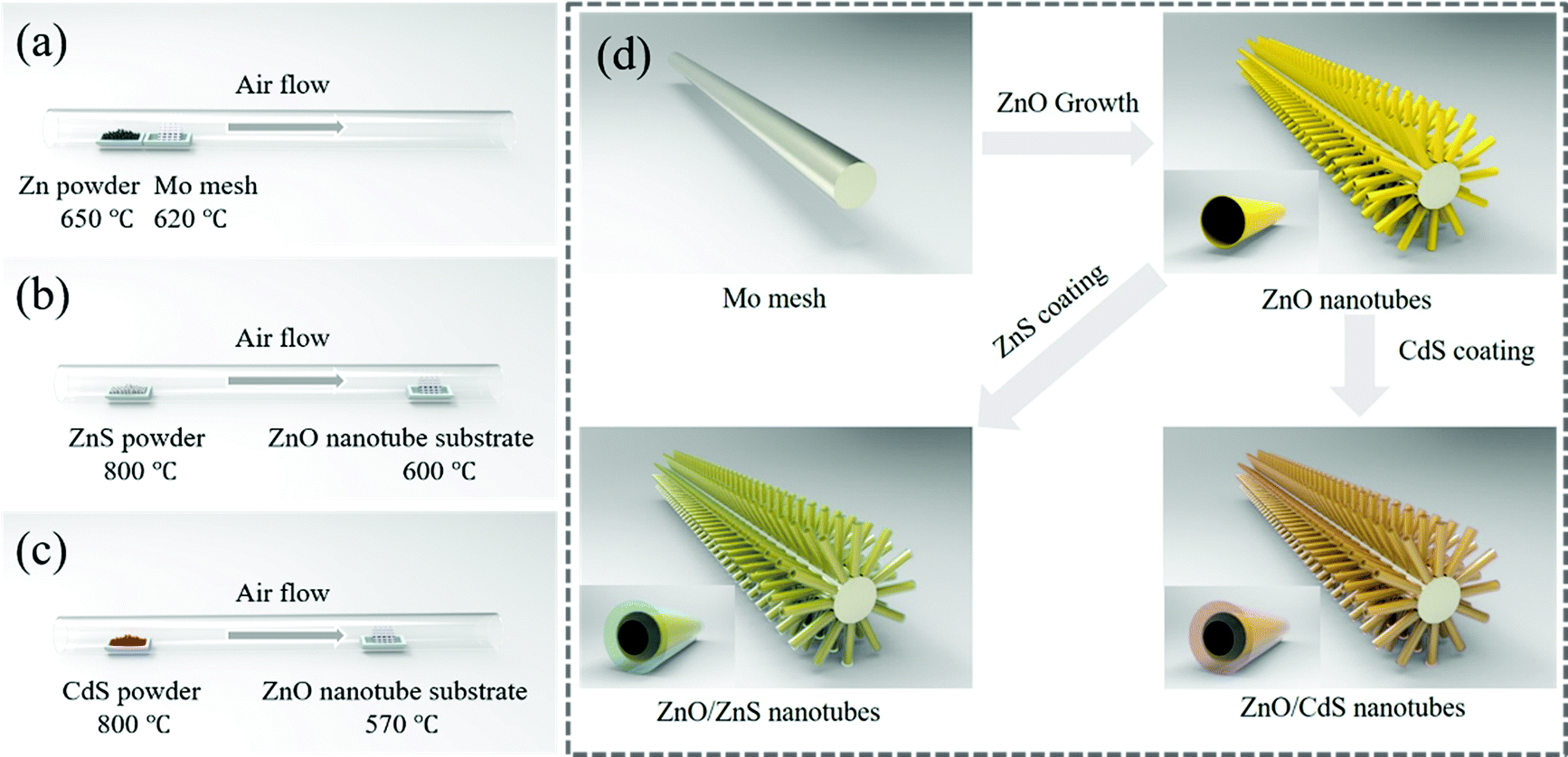 | ||
| Fig. 1 Experimental setup for the synthesis of (a) ZnO, (b) ZnO/ZnS and (c) ZnO/CdS nanotube arrays in a horizontal tube furnace; (d) schematic growth process of ZnO, ZnO/ZnS and ZnO/CdS nanotube arrays. | ||
Fig. 2a and b respectively show the low- and high-magnification SEM images of the obtained ZnO product. It presents a brush-like morphology with individual nanostructures grown radially along the surface of the Mo wire. Fig. 2c shows the SEM image of a single ZnO nanostructure. It is interesting to find that the object shows a tubular structure. The length of those nanotubes is about 5–10 μm with their outer diameter in the range of 150–200 nm, typically. It is also noteworthy that some of the nanotubes show a pentagonal cross section (Fig. 2c). Fig. 2d is the energy-dispersive X-ray spectrometry (EDX) spectrum of the sample. It only shows signals of Zn and O with an atomic ratio of about 1![[thin space (1/6-em)]](https://www.rsc.org/images/entities/char_2009.gif) :1, indicating the composition of ZnO. The atomic structure of the ZnO nanotube is further examined by transmission electron microscopy (TEM). Fig. 2e shows the TEM image of the nanotube. Due to its tubular structure, the side wall of the nanotube shows a relatively dark contrast in TEM imaging. Fig. 2f shows the HRTEM image of a nanotube. The lattice fringes with a measured interplanar distance of about 0.52 nm match well with the (0001) planes of wurtzite (WZ) ZnO. The inset of Fig. 2d shows the corresponding selected-area electron diffraction (SAED) pattern. The presence of well-aligned diffraction spots signifies the single-crystalline nature of the tube. The spots appear sharp and intense, which is an indication that the tube grows with good crystallinity.
:1, indicating the composition of ZnO. The atomic structure of the ZnO nanotube is further examined by transmission electron microscopy (TEM). Fig. 2e shows the TEM image of the nanotube. Due to its tubular structure, the side wall of the nanotube shows a relatively dark contrast in TEM imaging. Fig. 2f shows the HRTEM image of a nanotube. The lattice fringes with a measured interplanar distance of about 0.52 nm match well with the (0001) planes of wurtzite (WZ) ZnO. The inset of Fig. 2d shows the corresponding selected-area electron diffraction (SAED) pattern. The presence of well-aligned diffraction spots signifies the single-crystalline nature of the tube. The spots appear sharp and intense, which is an indication that the tube grows with good crystallinity.
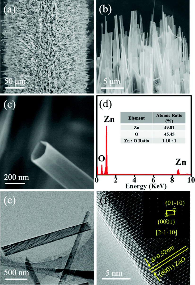 | ||
| Fig. 2 (a) Low- and (b) high-magnification SEM images of ZnO nanotube arrays grown on Mo mesh; (c) SEM image of a single ZnO nanotube; (d) EDX spectrum of ZnO nanotubes. The inset shows the atomic ratio of the sample; (e) TEM image of a single ZnO nanotube; (f) HRTEM image and the corresponding SAED pattern of the ZnO nanotube. | ||
As far as we know, growth of ZnO nanotube arrays through a CVD process is rarely reported. Considering their potential uses as building blocks in assembling novel optoelectronic devices, it is thus of crucial importance to clarify the growth mechanism of the ZnO nanotube arrays. We notice in the product that some nanotubes show a solid nanorod base, as shown in Fig. 3a. Such kinds are supposed to be in a transition stage towards the formation of ZnO nanotubes.42 EDX analysis reveals that the solid base is composed of nonstoichiometric metastable zinc-rich ZnOx (x < 1). It is well known that metastable ZnOx has a much lower melting point (419 °C) compared to stoichiometric ZnO.42 Therefore, we assume that the upper tubular part probably forms as a result of evaporation of the inner low-melting-point ZnOx during an increase in temperature. According to the above analysis, the growth mechanism of the ZnO nanotube arrays is proposed as follows. At the beginning, due to the relatively low temperature and insufficient supply of air, the vaporized Zn gas cannot be fully oxidized, resulting in the formation of metastable Zn rich ZnOx nanoparticles on the surface of Mo wire mesh. Due to the low chemical potential, those metastable ZnOx particles will keep adsorbing the incoming vapor and serve as the nucleus for subsequent growth of ZnOx nanorods. With an elevated temperature, two spontaneous processes are likely to occur which are the following: surface oxidation of the grown ZnOx nanorods to form a stable ZnO shell and decomposition of the inner metastable ZnOx to form a hollow structure. After those processes, an intermediate structure composed of segments of nanorods (at the base) and nanotubes (at the top) is formed. Once the tubular structures are formed, they will serve as the substrate for the homoepitaxial growth of the nanotubes along the longitudinal axis. The schematic formation process of the ZnO nanotube is illustrated in Fig. 3b. As we mentioned above that with most of the nanorods showing cylindrical shape, some tend to form pentagons. The reason for this is not clear yet. We consider that it is probably a joint result of kinetic and thermodynamic factors. It is also worth mentioning that utilization of Mo wire mesh with a high surface area and relatively rough surface gives rise to successful nucleation events compared to utilization of the commonly used Si wafer with a smooth surface,42 leading to the growth of nanostructures with a high density and good uniformity.
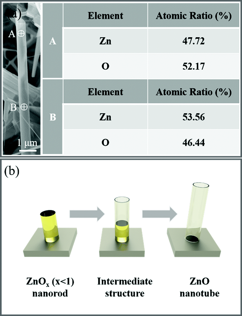 | ||
| Fig. 3 (a) EDX analysis at different sites of a nanotube. A depicts the nanotube part and B depicts the nanorod part; (b) schematic illustration of the growth process of ZnO nanotubes. | ||
Previous reports have shown the potential use of 1D ZnO nanostructures as functional components in optoelectronic and photovoltaic devices.8,9,11,12 However, the performance of such devices is largely limited by the short life time of photoexcited electrons and holes in ZnO nanostructures. Recently, both experimental and theoretical studies have demonstrated that by surface decoration of an additional semiconductor on ZnO to form type-II heterostructures, the performance of devices from those heterostructures can be significantly improved.27–29,38–41 The formation of a type-II band alignment can efficiently decrease the recombination rate of electrons and holes; correspondingly, their life time can be largely expanded.43,44 Motivated by this, ZnS and CdS, with proper band positions in reference to ZnO, were chosen as the deposition materials, aiming to form type-II heterostructures with pre-prepared ZnO nanotubes. Fig. 4a and b show the SEM and TEM images of a single ZnO nanotube after the deposition of ZnS. In comparison with the pristine ZnO nanotube showing a relatively smooth surface (Fig. 2c and e), the surface of the tube afterwards becomes slightly rougher. In addition, the wall thickness of the tube also shows a notable increase from 5–10 nm to 20–50 nm. These observations signify the possible growth of ZnS on the ZnO tubes. To confirm the composition of the product, we carried out EDX analysis coupled with SEM. As exhibited in Fig. 4c, the EDX spectrum reveals the presence of Zn, O and S elements in the sample with an atomic ratio of 1.1:1:0.1. The element mapping image vividly shows (Fig. 4d) that the O signal is mainly confined in the core region of the nanotube while the Zn and S signals are distributed throughout the entire nanotube. Structural analysis of the grown layer is also performed by TEM. The HRTEM image in Fig. 4e clearly resolves lattice fringes with a d-spacing of 0.62 nm, coinciding well with the (0001) planes of WZ ZnS. Of note, some lattice fringes in the ZnS layer are strongly distorted. This is because of the large lattice mismatch between ZnO and ZnS (20%) that causes strong stress during ZnS growth. Gradual release of the stress results in distortion of the crystal lattice in the grown ZnS layer. By introducing crystal imperfection, the single-crystalline nature of the epitaxial ZnS layer is preserved somehow. Fig. 4f shows the corresponding SAED pattern. Two sets of diffraction spots are revealed, which can be indexed to WZ ZnO and WZ ZnS, respectively, with a common zone axis of [2-1-10]. Interestingly, the two components within the heterostructure show an epitaxial relationship despite the large lattice mismatch, that is, [0001]ZnS//[0001]ZnO and (01-10)ZnS//(01-10)ZnO.
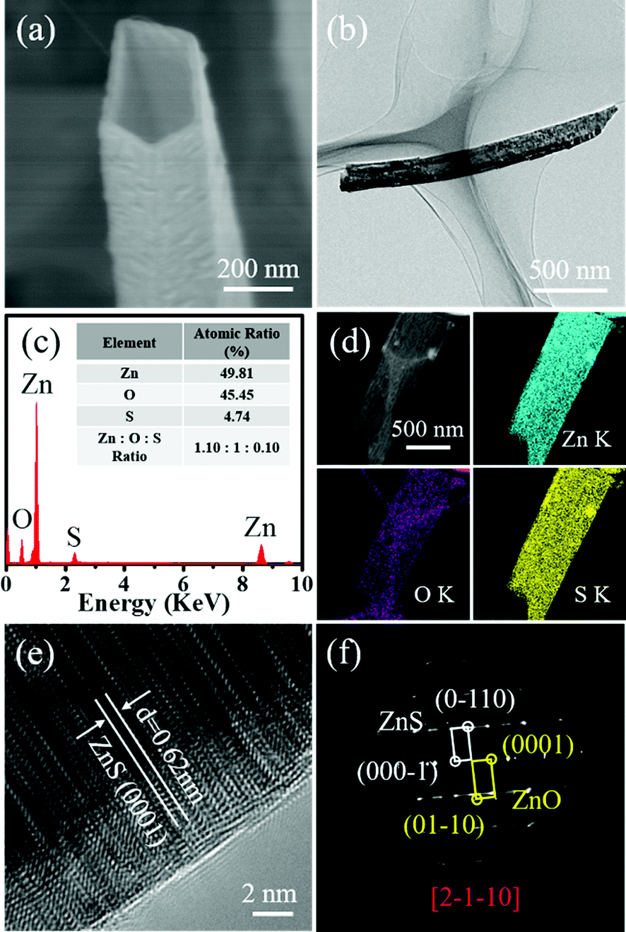 | ||
| Fig. 4 (a) SEM image and (b) TEM image of a single ZnO nanotube after coating of ZnS; (c) EDX spectrum of the nanotubes. The inset depicts the atomic ratio of the nanotubes; (d) Annular dark-field (ADF) image and the corresponding element mapping images; (e) HRTEM image of the nanotubes after deposition of ZnS; (f) The corresponding SAED pattern. | ||
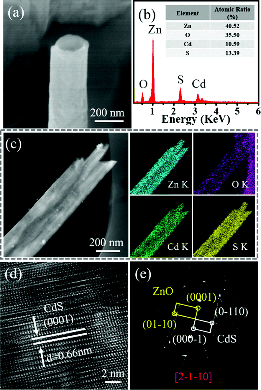
Similarly, the epitaxial method was also used to deposit CdS on the ZnO nanotube arrays. The SEM image of the product after CdS coating is shown in Fig. 5a. Clearly, the nanotube presents a relatively rougher surface and thicker wall compared with the ZnO nanotube, suggesting the possible growth of CdS on ZnO. The following composition analysis (Fig. 5b) as well as the elemental maps (Fig. 5c) solidly demonstrates the presence of CdS on ZnO. In order to study the atomic structure of the heterojunction, HRTEM and the corresponding SAED techniques were employed. Fig. 5d displays the HRTEM image of a nanotube, in which the lattice fringes with a measured distance of about 0.66 nm corresponds to the (0001) planes of WZ CdS. Similar to the previous case, lattice distortion was also observed in the CdS layer. Although the lattice mismatch between ZnO and CdS (27%) is even larger in this case, the grown CdS somewhat remains single-crystalline. The corresponding SAED pattern (Fig. 5e) shows superposition of two sets of diffraction spots from ZnO and CdS, which reveals an epitaxial relationship, i.e., [0001]CdS//[0001]ZnO and (01-10 )CdS//(01-10)ZnO. This is exactly the same as that indicated in the case of the ZnO/ZnS nanotubes. The identical epitaxial growth relationship is probably because of a common feature among ZnO, ZnS and CdS that they all exist in the WZ structure.
 | ||
| Fig. 5 (a) SEM image of a single ZnO nanotube after CdS coating; (b) EDX spectrum of the products; (c) ADF-STEM image and the corresponding elemental mapping images; (d) HRTEM image of the nanotube after deposition of CdS; (e) the corresponding SAED pattern. | ||
We have demonstrated above the successful surface modification of ZnO nanotubes with single-crystalline ZnS and CdS to form type-II heterostructures. In order to study the effect of surface engineering on the optical properties of the ZnO nanotubes, cathodoluminescence (CL) measurement was carried out on the samples at room temperature (Fig. 6). From the ZnO CL spectrum, two emission peaks are observed. The sharp and intense peak at ∼390 nm can be ascribed to the near band edge (NBE) emission of ZnO while the broad visible emission centered at ∼511 nm is commonly believed to relate to the defects of ZnO, such as oxygen vacancy and interstitial zinc.45 In comparison to the pure ZnO nanotube, however, the hybrids present strongly quenched CL emissions. Particularly for the NBE emission of ZnO, quenching of 67.2% and 99.7% is observed on ZnO/CdS and ZnO/ZnS, respectively.
 | ||
| Fig. 6 Cathodoluminescence spectra obtained from a single ZnO nanotube, ZnO/ZnS nanotube and ZnO/CdS nanotube. | ||
As charge transfer acts as an additional decay channel for charge carriers besides radiative recombination, we believe that pronounced reduction in CL emission is an indication of efficient charge separation ascribed from the type-II band alignment of the ZnO/ZnS and ZnO/CdS heterojunctions.44,46Fig. 7 illustrates the energy level diagrams of the ZnO/ZnS and ZnO/CdS heterostructures. As shown, the valence band and conduction band of ZnS and CdS are both energetically above the respective bands of ZnO, which is characteristic of type-II band alignment. Consequently, after the cathode-ray excitation and the charge transfer process, the electrons are mainly concentrated in the ZnO cores while the holes find their lowest energetic states in the ZnS and CdS shells.37 Thus, the overlap between the electron and hole wave function is small and the radiative recombination rate becomes significantly low, resulting in a great decrease in CL emission.
 | ||
| Fig. 7 Energy level diagrams of ZnO/ZnS and ZnO/CdS heterostructures as well as the charge transfer process under cathodoexcitation. | ||
Conclusions
In summary, we put forward a CVD method for fabricating single-crystalline ZnO nanotube arrays on the surface of Mo mesh. Based on detailed composition and morphology characterization, a rational mechanism for the growth of ZnO nanotube arrays is proposed. Subsequent growth of ZnS and CdS on the pre-fabricated ZnO nanotubes leads to the formation of ZnO/ZnS and ZnO/CdS heterostructures with a type-II band alignment. TEM analysis revealed that the ZnS and CdS are single-crystalline, which follow an epitaxial growth manner despite the large lattice mismatch between the grown components and ZnO. The epitaxial orientation relationship is identified as [0001]ZnS or CdS//[0001]ZnO and (10-10)ZnS or CdS//(10-10)ZnO. Room temperature CL spectra of the ZnO/ZnS nanotubes and ZnO/CdS nanotubes show dramatically reduced ZnO NBE emission and deep level emission compared with the bare ZnO nanotubes. Charge separation induced by type-II band alignment is believed to be responsible for the changes in optical properties. It is expected that the as-prepared nanotube arrays are highly promising candidates for optoelectronic and photocatalysis applications due to their single-crystalline nature, ordered alignment and efficient charge separation. This simple CVD technique may also be used to synthesize other semiconductor nanotube arrays and epitaxial heterostructures.Acknowledgements
We thank the “Strategy Priority Research Program” of Chinese Academy of Sciences (Grant No. XDA09040203) and 973 Project (2012CB932401) for financial support.Notes and references
- M. N. Newton, S. J. Leake, R. Harder and I. K. Robinson, Nat. Mater., 2010, 9, 279–279 CrossRef CAS PubMed.
- R. F. Service, Science, 2013, 339, 263–263 CrossRef CAS PubMed.
- L. F. Hu, J. Yan, Y. Kim, G. T. Fei, K. Watanabe, T. Sekiguchi, L. D. Zhang and X. S. Fang, Small, 2015, 11, 1531–1536 CrossRef CAS PubMed.
- K. P. Gong, F. Du, Z. H. Xia, M. Durstock and L. M. Dai, Science, 2009, 323, 760–764 CrossRef CAS PubMed.
- J. Jie, W. Zhang, I. Bello, C.-S. Lee and S.-T. Lee, Nano Today, 2010, 5, 313–336 CrossRef CAS.
- Y. N. Xia, P. D. Yang, Y. G. Sun, Y. Y. Wu, B. Mayers, B. Gates, Y. D. Yin, F. Kim and Y. Q. Yan, Adv. Mater., 2003, 15, 353–389 CrossRef CAS.
- T. Zhai, L. Li, X. Wang, X. S. Fang, Y. Bando and D. Golberg, Adv. Funct. Mater., 2010, 20, 4233–4248 CrossRef CAS.
- H.-Y. Shin, E.-L. Shim, Y.-J. Choi, J.-H. Park and S. Yoon, Nanoscale, 2014, 6, 14622–14626 RSC.
- S. Xu and Z. L. Wang, Nano Res., 2011, 4, 1013–1098 CrossRef CAS.
- X. Huang, J. Xia, C. Luan, M. Sun, X. Wang, G.-W. She, C.-S. Lee and X.-M. Meng, CrystEngComm, 2013, 15, 10604–10610 RSC.
- Y. J. Hong, H. S. Jung, J. Yoo, Y. J. Kim, C. H. Lee, M. Kim and G. C. Yi, Adv. Mater., 2009, 21, 222–226 CrossRef CAS.
- Y. J. Hong, J.-M. Jeon, M. Kim, S.-R. Jeon, K. H. Park and G.-C. Yi, New J. Phys., 2009, 11, 125021 CrossRef.
- L. Xu, Q. Liao, J. Zhang, X. Ai and D. Xu, J. Phys. Chem. C, 2007, 111, 4549–4552 CAS.
- C. C. Wu, D. S. Wuu, P. R. Lin, T. N. Chen and R. H. Horng, Cryst. Growth Des., 2009, 9, 4555–4561 CAS.
- S. L. Mensah, V. K. Kayastha, I. N. Ivanov, D. B. Geohegan and Y. K. Yap, Appl. Phys. Lett., 2007, 90, 113108 CrossRef.
- J. Yoo, Y. J. Hong, H. S. Jung, Y.-J. Kim, C.-H. Lee, J. Cho, Y.-J. Doh, L. S. Dang, K. H. Park and G.-C. Yi, Adv. Funct. Mater., 2009, 19, 1601–1608 CrossRef CAS.
- A. Prasad, S. Mensah, J. Wang, A. Pandey and Y. K. Yap, Materials Research Society Proceedings, 2007, 1057 Search PubMed.
- G. She, X. Huang, L. Jin, X. Qi, L. Mu and W. Shi, Small, 2014, 10, 4685–4692 CrossRef CAS PubMed.
- L. L. Yang, Z. Q. Zhang, J. H. Yang, Y. S. Yan, Y. F. Sun, J. Cao, M. Gao, M. B. Wei, J. H. Lang, F. Z. Liu and Z. Wang, J. Alloys Compd., 2012, 543, 58–64 CrossRef CAS.
- C. Q. Zhu, B. A. Lu, Q. Su, E. Q. Xie and W. Lan, Nanoscale, 2012, 4, 3060–3064 RSC.
- F.-X. Xiao, ACS Appl. Mater. Interfaces, 2012, 4, 7055–7063 CAS.
- Y. J. Wang, R. Shi, J. Lin and Y. F. Zhu, Energy Environ. Sci., 2011, 4, 2922–2929 CAS.
- Z. Chen, N. Zhang and Y. J. Xu, CrystEngComm, 2013, 15, 3022–3030 RSC.
- J. Schrier, D. O. Demchenko and L. W. Wang, Nano Lett., 2007, 7, 2377–2382 CrossRef CAS PubMed.
- A. Torabi and V. N. Staroverov, J. Phys. Chem. Lett., 2015, 6, 2075–2080 CrossRef CAS PubMed.
- S. Muthulingam, K. Bin Bae, R. Khan, I. H. Lee and P. Uthirakumar, RSC Adv., 2015, 5, 46247–46251 RSC.
- J. K. Kim, S. Bae, W. Kim, M. J. Jeong, S. H. Lee, C. L. Lee, W. K. Choi, J. Y. Hwang, J. H. Park and D. I. Son, Nano Energy, 2015, 13, 258–266 CrossRef CAS.
- A. Baranowska-Korczyc, K. Sobczak, P. Dluzewski, A. Reszka, B. J. Kowalski, L. Klopotowski, D. Elbaum and K. Fronc, Phys. Chem. Chem. Phys., 2015, 17, 24029–24037 RSC.
- S. C. Rai, K. Wang, Y. Ding, J. K. Marmon, M. Bhatt, Y. Zhang, W. L. Zhou and Z. L. Wang, ACS Nano, 2015, 9, 6419–6427 CrossRef CAS PubMed.
- Y. Zhang, H. L. Lu, T. Wang, Q. H. Ren, Y. Z. Gu, D. H. Li and D. W. Zhang, Nanoscale, 2015, 7, 15462–15468 RSC.
- X. Huang, M. Wang, M. G. Willinger, L. D. Shao, D. S. Su and X. M. Meng, ACS Nano, 2012, 6, 7333–7339 CrossRef CAS PubMed.
- X. D. Wang, P. X. Gao, J. Li, C. J. Summers and Z. L. Wang, Adv. Mater., 2002, 14, 1732–1735 CrossRef CAS.
- W. Tian, C. Zhang, T. Y. Zhai, S. L. Li, X. Wang, J. W. Liu, X. Jie, D. Q. Liu, M. Y. Liao, Y. Koide, D. Golberg and Y. Bando, Adv. Mater., 2014, 26, 3088–3093 CrossRef CAS PubMed.
- Z. K. Zheng, W. Xie, Z. S. Lim, L. You and J. L. Wang, Sci. Rep., 2014, 4, 6 Search PubMed.
- Q. Yang, Y. Li, Z. Hu, Z. Duan, P. Liang and J. Sun, N. Xu and J. Wu, Opt. Express, 2014, 22, 8617–8623 CrossRef CAS PubMed.
- X. W. Wang, L. C. Yin, G. Liu, L. Z. Wang, R. Saito, G. Q. Lu and H. M. Cheng, Energy Environ. Sci., 2011, 4, 3976–3979 CAS.
- S. S. Lo, T. Mirkovic, C.-H. Chuang, C. Burda and G. D. Scholes, Adv. Mater., 2011, 23, 180–197 CrossRef CAS PubMed.
- X. Huang, Y. Q. Yu, J. Xia, H. Fan, L. Wang, M. G. Willinger, X. P. Yang, Y. Jiang, T. R. Zhang and X. M. Meng, Nanoscale, 2015, 7, 5311–5319 RSC.
- J. Xu, X. Yang, H. K. Wang, X. Chen, C. Y. Luan, Z. X. Xu, Z. Z. Lu, V. A. L. Roy, W. J. Zhang and C. S. Lee, Nano Lett., 2011, 11, 4138–4143 CrossRef CAS PubMed.
- F. Schuster, B. Laumer, R. R. Zamani, C. Magen, J. R. Morante, J. Arbiol and M. Stutzmann, ACS Nano, 2014, 8, 4376–4384 CrossRef CAS PubMed.
- K. Bulashevich, I. Y. Evstratov and S. Y. Karpov, Phys. Status Solidi A, 2007, 204, 241–245 CrossRef CAS.
- Y. Xing, Z. Xi, X. Zhang, J. Song, R. Wang, J. Xu, Z. Xue and D. Yu, Solid State Commun., 2004, 129, 671–675 CrossRef CAS.
- R. Mahadevu, A. R. Yelameli, B. Panigrahy and A. Pandey, ACS Nano, 2013, 7, 11055–11063 CrossRef CAS PubMed.
- D. Gross, A. S. Susha, T. A. Klar, E. Da Como, A. L. Rogach and J. Feldmann, Nano Lett., 2008, 8, 1482–1485 CrossRef CAS PubMed.
- H. Zeng, G. Duan, Y. Li, S. Yang, X. Xu and W. Cai, Adv. Funct. Mater., 2010, 20, 561–572 CrossRef CAS.
- K. Wang, J. Chen, Z. Zeng, J. Tarr, W. Zhou, Y. Zhang, Y. Yan, C. Jiang, J. Pern and A. Mascarenhas, Appl. Phys. Lett., 2010, 96, 123105 CrossRef.
| This journal is © The Royal Society of Chemistry 2016 |