
 Open Access Article
 This Open Access Article is licensed under a
 Creative Commons Attribution 3.0 Unported Licence
Rapid vapour deposition and in situ melt crystallization for 1 min fabrication of 10 μm-thick crystalline silicon films with a lateral grain size of over 100 μm†
Y.
Yamasaki
,
K.
Hasegawa
,
T.
Osawa
and
S.
Noda
*
Department of Applied Chemistry, Waseda University, 3-4-1 Okubo, Shinjuku-ku, Tokyo 169-8555, Japan. E-mail: noda@waseda.jp
First published on 6th April 2016
Abstract
We developed a film deposition method which yielded continuous polycrystalline Si films with large lateral grain sizes of over 100 μm and thicknesses of ∼10 μm in 1 min on growth substrates other than silicon wafers in a single-step process. The silicon source is heated to ∼2000 °C, much higher than the melting point of Si, which enables a high deposition rate. Controlling the temperature of the growth substrate, initially above and later below the melting point of Si, allows the seamless lateral to vertical growth of crystalline silicon grains. Thermally and chemically stable substrates of quartz glass and alumina with a 0.1 μm-thick amorphous carbon layer were effective; liquid silicon wetted well by forming a thin SiC interlayer while substrates stayed stable. Such large-grain polycrystalline silicon films synthesized rapidly in 1 min may be used for low-cost, stable and flexible thin film photovoltaic cells.
Introduction
Crystalline silicon (Si) wafers and films are supporting our society as key parts of many electronic devices such as semiconductor integrated circuits (ICs), thin-film transistors in flat-panel displays (FPDs) and photovoltaic (PV) cells. The production processes of crystalline Si can be classified into two types; one is wafer production by wire-saw slicing of mono- or polycrystalline ingots made from molten Si,1 and the other is thin-film deposition on growth substrates by chemical vapour deposition (CVD) of Si precursor gases.2,3 Monocrystalline Si wafers, which are high-quality, high-performance and expensive, are indispensable for ICs. Polycrystalline Si wafers or films having larger in-plane grain sizes than the thicknesses, which we call large-grain Si hereafter, have been used as fundamental parts of large-area devices such as PV cells and FPDs.4,5The fabrication processes of large-grain Si films on substrates can be divided by the type of growth substrate: monocrystalline Si substrates and other substrates. Monocrystalline Si films can easily grow on monocrystalline Si substrates through homoepitaxy by CVD, physical vapour deposition, liquid-phase epitaxy and other methods. However, Si films need to be transferred to low-cost carrier substrates (e.g. plastic or glass) in a successive process for cost reduction.3,6,7 The growth substrate and the homoepitaxial film have the same crystal structure, orientation and chemical properties, and therefore it is difficult to separate the film from the growth substrate (i.e. Si wafer). Sacrificial heteroepitaxial interlayers such as CoSi2 have been reported,8 but the transfer process is complicated. Methods need to be established for easy separation of the films from growth substrates and reuse of growth substrates.
Growth substrates other than monocrystalline Si, such as SiO2, are attractive in the viewpoint of the separation of films and substrates. On most of such substrates, Si does not grow epitaxially. Si forms either amorphous films on substrates below its crystallization temperature9 or polycrystalline films on substrates above its crystallization temperature.10,11 In polycrystalline film growth, each nucleus has a different orientation and generally grows isotopically, comes in contact with other growing nuclei and forms continuous films. Then, each nucleus/grain grows in the out-of-plane direction, yielding polycrystalline films with a lateral grain size smaller than the thickness. To obtain polycrystalline films with large grains (i.e. lateral grain size larger than the film thickness), films are post-treated by laser or lamp annealing12–14 to cause lateral grain growth through melting and (re)crystallization processes. In particular, the zone melting recrystallization (ZMR) method can enlarge grains in several micrometre-thick films from the micrometre scale to the centimetre scale by sweeping a heater and thus producing several millimetre-wide molten zones at sweep rates of a few centimetres per minute.15 However, the ZMR process is accompanied with agglomeration of molten Si, the so-called balling-up effect, as a result of surface tension, and therefore Si films have to be covered with a SiO2 capping layer to prevent agglomeration.15,16 Among these processes, the excimer laser annealing process has been used for the production of FPDs.5 However, none of these methods have been practically used for the production of low-cost PV cells. The ribbon Si process, which coats and crystallizes molten Si on heat-resisting substrates, can be used to fabricate large-grain polycrystalline Si films of around 100 μm in thickness,17–19 but further thinning is difficult because of the surface tension of molten Si.
In this report, we propose and develop a new method called “rapid vapour deposition (RVD) of liquid Si and in situ melt crystallization”, which yields large-grain polycrystalline Si films directly on heat-resistant substrates other than monocrystalline Si in a single-step process. RVD is a vacuum deposition process realizing a high deposition rate of over 10 μm min−1 by heating a Si source in boats to Tboat ∼ 2000 °C, which is much higher than the melting point of Si, Tm = 1414 °C.20 During RVD, the substrate temperature Tsub is intentionally changed in a controlled manner; Tsub is set at >Tm for the first several seconds to deposit Si as a liquid film, and subsequently Tsub is decreased to <Tm to nucleate Si crystals and grow them laterally in the liquid film, and finally thickening the film to ∼10 μm by continuing the deposition of Si vapours. All these steps are completed seamlessly in one process within 1 min, yielding 10 μm-thick crystalline Si films with a lateral grain size of over 100 μm on a heat-resistant quartz-glass and alumina substrate with a 0.1 μm-thick amorphous carbon (a-C) adhesive layer.
Experimental
Quartz glass (SiO2; 15 mm square, 0.5 mm in thickness), monocrystalline (100) Si wafer with a 50 nm-thick thermal oxide layer (SiO2/Si; 20 mm square, 0.65 mm in thickness, Cz-p type, resistivity of 10–20 Ω cm), polycrystalline alumina (Al2O3; 15 mm square, 1 mm in thickness) (Nilaco AL-017518, Tokyo, Japan), or sapphire (c-plane, 20 mm square, 0.3 mm in thickness) (Kyocera, Kyoto, Japan) were used as substrates. The substrates were pre-treated by immersing them into a mixed solution of H2SO4 (95 wt%) and H2O2 (30 wt%) with a volume ratio of 3![[thin space (1/6-em)]](https://www.rsc.org/images/entities/char_2009.gif) :1 for 5 min, and then rinsing them with purified water. The pre-treated monocrystalline Si substrates were subsequently dipped in HF solution (5 wt%) for 1 min to partially remove the thermal oxide from half of their surface, and were then rinsed with purified water. A 0.1 μm-thick a-C layer was deposited on some substrates by direct current magnetron sputtering under 2.5 Pa Ar. For RVD, (100) Si wafer (3.5 × 30 mm2, 0.65 mm in thickness, Cz-p type, resistivity of 10–20 Ω cm) was used as the vapour deposition source after pre-treatment by immersion in HF solution (5 wt%) for 1 min and rinsing with purified water.
:1 for 5 min, and then rinsing them with purified water. The pre-treated monocrystalline Si substrates were subsequently dipped in HF solution (5 wt%) for 1 min to partially remove the thermal oxide from half of their surface, and were then rinsed with purified water. A 0.1 μm-thick a-C layer was deposited on some substrates by direct current magnetron sputtering under 2.5 Pa Ar. For RVD, (100) Si wafer (3.5 × 30 mm2, 0.65 mm in thickness, Cz-p type, resistivity of 10–20 Ω cm) was used as the vapour deposition source after pre-treatment by immersion in HF solution (5 wt%) for 1 min and rinsing with purified water.
Fig. 1 shows a digital image and a schematic of the internal structure of the RVD apparatus. The components were set from bottom to top as follows: two tungsten boats for the Si source, a substrate stage made of quartz glass, a W0.95Re0.05–W0.74Re0.26 thermocouple, a substrate heater made of a graphite sheet and four reflectors made of molybdenum sheets. After setting a substrate on the stage with its surface facing down and the Si source on the boats, the chamber was evacuated to <3 × 10⁻⁴ Pa using a turbomolecular pump with an oil rotary pump. The substrate heater was turned on to make the thermocouple reach a target temperature, and then RVD was carried out by resistive heating of the source boats to ∼2000 °C in several seconds. Si was deposited for 1 min, and after that, heating of the source boats was turned off to finish the deposition.
 | ||
| Fig. 1 Digital image (a) and schematic (b) of the inner structure of the RVD apparatus. | ||
The structure of the Si films was analysed by scanning electron microscopy (SEM; Hitachi S-4800, Tokyo, Japan) and X-ray diffraction (XRD; Rigaku RINT-TTR III, Tokyo, Japan) with a monochromatised CuKα X-ray source.
Results and discussion
The proposed model with typical results of the deposition method and comparison with conventional methods
Fig. 2 shows a schematic comparing the film growth processes by our deposition method and the conventional deposition method. In common methods such as vacuum deposition or CVD, a substrate is kept at a constant temperature with Tsub < Tm during deposition (Fig. 2b). On a substrate in which epitaxial growth does not occur (e.g. SiO2), Si atoms form small nuclei that grow in the out-of-plane direction and form columnar grains. Grains oriented in the fastest growth direction grow preferentially, often resulting in increasing surface roughness with film growth. However, in our method, Si is deposited on a substrate set at Tsub > Tm, condensing on the substrate to form a liquid film (Fig. 2a). Although Si re-evaporates from the liquid film, the Si source heated at Tboat ≈ 2000 °C ≫ Tm yields a much higher vapour pressure than the liquid film, realizing a deposition rate which is much larger than the re-evaporation rate and the deposition of the liquid film. Then, we lower the Tsub value to <Tm to nucleate Si crystallites from the liquid film, inducing lateral grain growth of planar grains in the liquid film, and thickening the film to ∼10 μm by continuing the vapour deposition. Through this growth model, we tried to obtain large-grain polycrystalline Si films in 1 min. | ||
| Fig. 2 Film growth processes proposed for our method (a) and known for the conventional vapour deposition method (b). | ||
Fig. 3 shows a typical Si film deposited on a 0.1 μm a-C/SiO2 substrate using our method. Fig. 3a shows the time profile of the temperature of the thermocouple, TTC; the deposition was started at 0 s with TTC > Tm, TTC was quickly decreased to TTC < Tm at 5–20 s by decreasing the input power for the substrate heater, TTC was kept almost constant for 20–60 s, and then heating of the boats was turned off at 60 s, resulting in a further decrease in TTC at 60–70 s. The thermocouple was not in contact with the substrate to avoid temperature distribution in the substrate, and therefore, TTC has some deviation from Tsub and is used as a reference. We made a reference experiment to measure Tsub using a 0.1 μm a-C/SiO2 substrate with a Pt–Pt0.87Rh0.13 thermocouple fixed at the centre of the substrate. We carried out the RVD process with the same time profile of input power for the tungsten boats and the carbon heater but without putting the Si source material in the boats. As shown in the ESI,† Fig. S1, Tsub proved to be 100–150 °C lower than TTC, and slightly above the melting point of Si (Tm = 1414 °C) when the RVD process was started. Tsub decreased below Tm by decreasing the heating power for the upper carbon heater at 5 s. The digital image of the sample in Fig. 3b shows that Si was deposited on the inner 13 mm square area of the 15 mm square substrate and showed a silver-grey colour with patterns coming from the 100 μm grains. The surface and cross-sectional SEM images of the Si film in Fig. 3c and d show that a Si film with a lateral grain size of over 100 μm and a thickness of 10 μm was actually obtained rapidly in 1 min by our deposition method. The out-of-plane XRD pattern of the Si film in Fig. 3e shows the diffraction peaks from a diamond structure without any preferred orientation. The intensity ratios were different from the powder pattern and changed with the measurement point because only a limited number of the large Si grains (over 100 μm) were detected in each XRD measurement.
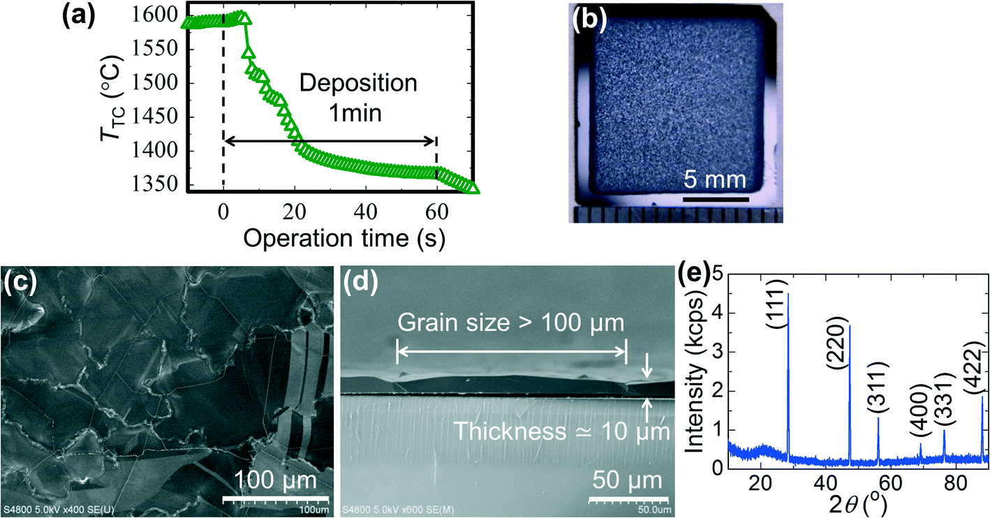 | ||
| Fig. 3 Representative results of the Si film deposited by our method. (a) Time profile of the temperature during deposition. (b) Digital image, (c) surface SEM image, (d) cross-sectional SEM image and (e) ω–2θ-scan XRD spectrum of a Si film deposited on the a-C/SiO2 substrate. | ||
We next show the growth behaviour of Si films at a temperature of TTC ∼ 1100 °C < Tm with a fixed substrate heater power. Fig. 4a shows a digital image of the sample deposited on the SiO2/Si(100) substrate with SiO2 removed by HF from half of its surface. The Si film deposited on SiO2 had a cloudy white surface whereas the Si film deposited on Si(100) had a mirror surface. The surface SEM images showed sub-micrometre-sized grains for the Si film on SiO2 (Fig. 4b) and a flat surface without any texture for the Si film on Si(100) (Fig. 4c). The cross-sectional SEM images showed columnar grains for the Si film on SiO2 (Fig. 4d) and a flat cross-section without any texture or boundary with the substrate for the Si film on Si(100) (Fig. 4e). The low-magnification cross-sectional SEM image near the boundary between SiO2/Si and Si showed a clear change in the Si film structure and rapid deposition of 16 μm in 1 min (Fig. 4f). The out-of-plane XRD spectrum of the Si film on SiO2/Si in Fig. 4g shows a prominent (400) peak coming from the Si(100) substrate with a forbidden (200) peak, which is characteristic of monocrystalline Si.21 In addition, (111), (220) and (331) peaks are observed, and therefore, the film is polycrystalline Si without any specific orientation in the out-of-plane direction. The Si film on Si(100) showed the same XRD spectra as the Si(100) substrate; the out-of-plane XRD spectrum showed only (400) and (200) peaks (Fig. 4h) and the Φ scan of the (022) diffraction showed a four fold symmetry (Fig. 4i). These results prove that the Si film grew by homoepitaxy on the Si(100) substrate. Our RVD method realized the rapid growth of Si films at 16 μm min−1 owing to the high Tboat ∼ 2000 °C, as a homoepitaxial film on the Si(100) surface, possibly owing to the high mobility of Si adatoms at the high substrate temperature, and as a columnar polycrystalline film on a SiO2 surface.
 | ||
| Fig. 4 Typical results of Si films deposited on Si(100) substrates at TTC ∼ 1100 °C (<Tmp). (a) Digital image of the surface of a Si film deposited on a SiO2/Si substrate with the thermal oxide layer being removed from half of its surface by HF. Surface (b, c) and cross-sectional (d, e) SEM images of the Si film deposited on SiO2/Si (b, d) and Si (c, e). (f) Cross-sectional SEM image of the Si film near the boundary between SiO2/Si and Si regions. (g–i) XRD spectra: ω–2θ scan (g) of a Si film deposited on a SiO2/Si(100) substrate and ω–2θ scan (h) and Φ scan (i) of a Si film deposited on Si(100). The symbol * denotes the forbidden (200) diffraction characteristic of monocrystalline Si.21 | ||
As mentioned above, compared with the conventional vapour deposition method at a constant substrate temperature below the melting point, our method can yield Si films with a significantly different structure with planar large grains by changing the substrate temperature, starting from TTC (∼Tsub) > Tm and decreasing to TTC (∼Tsub) < Tm during deposition. The conditions for large-grain polycrystalline Si films are discussed in detail below.
Effect of cooling rate on the grain sizes of the Si films deposited on a-C/SiO2 substrates
Si films were deposited on a-C/SiO2 substrates with different cooling rates. Deposition was started with TTC > Tm and continued at the fixed substrate heater power for 5 s, and then the heater power was decreased at three different rates (Fig. 5a). The digital images of the surface (Fig. 5b–d) showed shinier surfaces with coarser patterns for the samples deposited with slower cooling rates. The SEM images of the surface (Fig. 5e–g) showed polycrystalline films with lateral grain sizes changing with the cooling rates, from ∼50 μm by fast cooling to >100 μm by slow cooling. The grain size of the deposited Si films changed with the cooling rate, similar to the ordinal crystal growth from molten Si.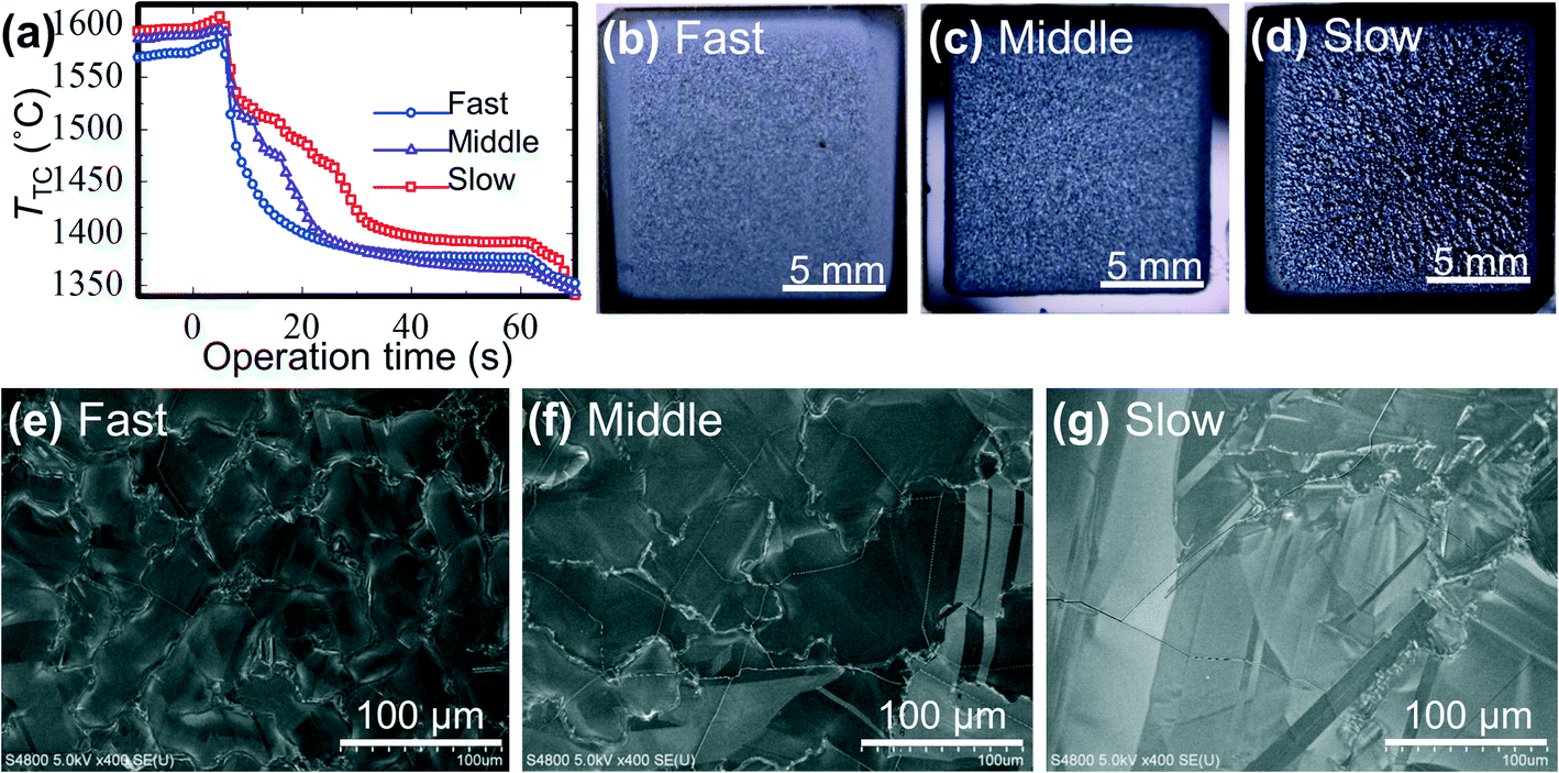 | ||
| Fig. 5 Si films deposited on a-C/SiO2 substrates at various cooling rates. (a) Time profiles of TTC for fast, middle and slow cooling. (b–d) Digital images and (e–g) SEM images of the surface of the Si films formed with different cooling rates. | ||
Si film growth on SiO2 substrates without the a-C layer
Fig. 6 shows a Si film deposited on the SiO2 substrate without the surface a-C layer. In the digital image (Fig. 6a), the part surrounded by red broken lines is the deposited area; however, a continuous Si film remained only on the grey-coloured central region of a 10 mm circle. A spherical particle with a diameter of ∼1 mm was found at the centre, which should have solidified from a Si droplet repelled from the SiO2 substrate. The SEM images of the surface and cross-section of the Si film at the central region showed a polycrystalline film with grain size as small as several micrometres (Fig. 6b and c). In the digital image (Fig. 6a), transparent SiO2 was exposed at the outer region. The surface and cross-sectional SEM images showed small spherical Si particles of ∼10 μm in diameter. Liquid Si should easily repel from and be discontinuous on the substrates with poor wettability.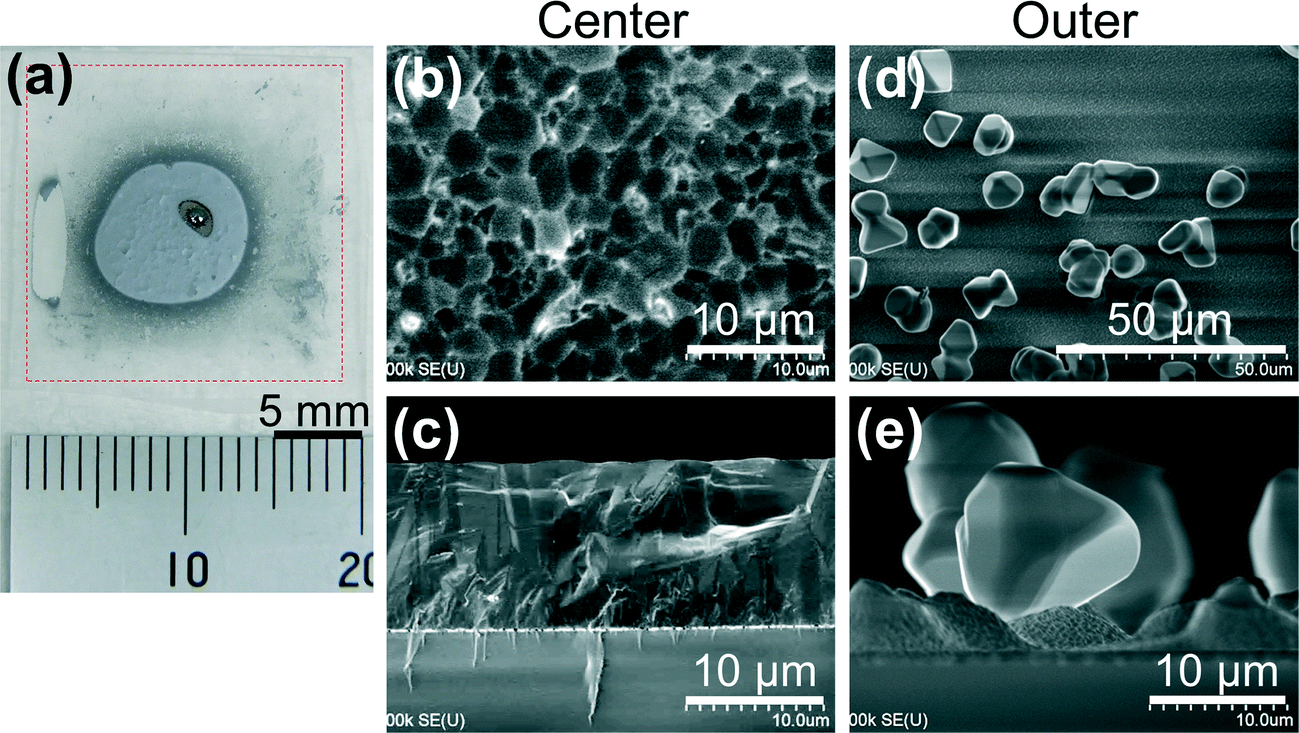 | ||
| Fig. 6 Si film deposited on a SiO2 substrate without the surface a-C layer. (a) Digital image of the surface. The square in red broken lines shows the Si deposition area. Surface (b, d) and cross-sectional (c, e) SEM images of the Si film at the central (b, c) and outer (d, e) regions. | ||
Conversely, the SiO2 substrates with a 0.1 μm-thick a-C surface layer yielded large-grain Si films uniformly over the deposited area as shown in Fig. 3 and 5. Next, we examined the very early stage of Si deposition on a-C/SiO2 to check the behaviour of Si on the a-C layer. We deposited Si for only 5 s, quickly cooled down the substrate, and then analysed the sample by SEM and XRD, as shown in Fig. 7. There are many droplet-like Si grains with smaller heights than the lateral dimensions and a much smaller wetting angle of ∼50° (Fig. 7c) than the SiO2 substrate without an a-C layer (Fig. 6e). The thin Si layer might have de-wetted during the cooling down process in this experiment of 5 s deposition. During actual deposition for 1 min, however, Si was depositing rapidly on the Si layer, and the thickening Si layer formed a continuous film without de-wetting on the substrate. Fig. 7d is the grazing-incidence XRD spectrum of this sample, which clearly shows the formation of β-SiC. Contact angles were previously reported for liquid Si on vitreous carbon (a-C) to be 40–50° at 1426 °C (ref. 22) and 36° at 1430 °C,23 which agree well with our observation (∼50°, Fig. 7c). A 0–100 nm a-C layer was previously applied to a microcrystalline alumina substrate to improve the wettability of Ni-63 at% Si alloy, where the formation of SiC was the key for the improved wettability.24 Thus, we conclude that a-C reacted with liquid Si and formed a β-SiC layer, on which liquid Si wetted well.
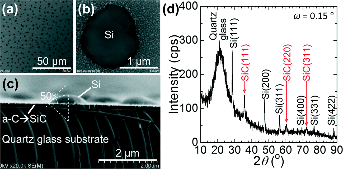 | ||
| Fig. 7 SEM images of a Si sample deposited on a-C/SiO2 for 5 s and cooled down immediately. Surface SEM images at low (a) and high (b) magnifications and a cross-sectional SEM image (c). Many hemispherical Si islands of a lateral size of approximately 1–2 μm were observed. (d) Grazing-incidence XRD spectrum taken with an incidence angle of ω = 0.15°. Three main peaks for β-SiC (ref. 25) were observed in addition to those for Si. | ||
As discussed above, Si formed continuous films with large grains on a-C because of the good wettability of Si with a-C. In contrast, Si had poor wettability with SiO2, yielding the repelled Si droplets and the discontinuous film of the solidified Si particles on the SiO2 substrate without an a-C layer. Because liquid Si reacts with an a-C layer to form SiC, it is important to have an a-C layer thin (0.1 μm) enough not to consume much Si by this reaction.
Effects of substrate materials: comparison of SiO2 and Al2O3 substrates
Residual stress between films and substrates can cause breaking and/or delamination of the films. In our method, a mismatch of the linear thermal expansion between the Si films and the substrates causes thermal stress during the cooling process. The linear thermal expansion of Si, fused SiO2, polycrystalline Al2O3, and a-axis Al2O3 at the temperature range of 20–1500 °C are estimated using previously reported equations26 and summarized in Fig. S2.† It clearly shows that fused SiO2 has the smallest value, Si has the medium value and Al2O3 has the largest value. Fig. 8 shows the Si films formed on a-C/SiO2 and a-C/Al2O3 substrates. Linear cracks can be seen on a-C/SiO2 at intervals of several tens of micrometres whereas no cracks were observed on a-C/Al2O3. Tensile stress worked on the Si film on a-C/SiO2 during cooling, resulting in crack formation. It should be important to choose appropriate substrates with thermal linear expansion similar to or somewhat larger than Si to obtain crack-free continuous Si films. | ||
| Fig. 8 Surface SEM images of the Si films deposited on SiO2 (quartz glass) (a–c), Al2O3 (polycrystalline alumina) (d–f) and Al2O3 (c-plane sapphire) (g–i) substrates having a 0.1 μm-thick a-C layer. Cracks were observed only in the Si film on the SiO2 substrate (a–c). | ||
Conclusions
We proposed a film deposition method, in which Si is rapidly deposited on a substrate heated above the melting point of Si and the substrate is subsequently cooled down below the melting point while maintaining rapid deposition. The method yielded continuous polycrystalline Si films with large lateral grain sizes of over 100 μm and thicknesses of ∼10 μm in 1 min in a single process on SiO2 and Al2O3 substrates with a 0.1 μm-thick a-C layer. To realize such films without using monocrystalline Si substrates, the choice of substrates is important. The substrates need to be thermally stable at temperatures above the Si melting point, chemically stable enough against liquid Si to be reusable, and in addition, need to have good wettability with liquid Si and to apply small/no tensile stress to the resulting Si films. An Al2O3 substrate with an a-C layer was a good combination, yielding crack-free continuous Si films with large grains owing to the good wettability of liquid Si with a-C via the reaction forming SiC and the larger thermal linear expansion of Al2O3 than Si (and thus compressive stress instead of tensile stress working on the resulting Si films).To practically produce Si films for real applications such as PV cells, how to avoid contamination to Si films at a high temperature and how to scale-up the process are the crucial issues. The maximum substrate temperature was slightly above the melting point of Si (Fig. S1†). This shows that our process has a similar temperature to but much shorter time than the ingot production process. Al is an effective dopant in making a back surface field in bulk Si PV cells27 and thus the Al2O3 substrate would be promising in avoiding the negative effects of contamination. For scale-up, we are planning a continuous process carrying growth substrates over a Si melt bath. It may be possible to directly convert Si melt in a crucible to Si films on Al2O3 with a takt time of ∼1 min, instead of making and slicing Si ingots into thick wafers in many hours/days. There is a long way to reach such goal, but this work should be the very important first step. As the next step, we are now working on a method to transfer large-grain Si films from a growth substrate to device substrates (glass and/or plastic) and reuse the growth substrate to achieve practical low-cost production of such Si films.
Acknowledgements
The authors thank Mr. Takahiro Goto at Materials Characterization Central Laboratory, Waseda University, for XRD analysis of the Si films. This work is financially supported in part by a Grant-in-Aid for Challenging Exploratory Research (15K14216) from the Japan Society for the Promotion of Science, Japan.References
- W. Koch, A. L. Endrös, D. Franke, C. Häßler, J. P. Kalejs and H. J. Möller, in Handbook of Photovoltaic Science and Engineering, ed. A. Luque and S. Hegedus, John Wiley & Sons, Ltd, Hoboken, 2003, ch. 6, pp. 218–254 Search PubMed.
- K. R. Catchpole, M. J. McCann, K. J. Weber and A. W. Blakers, Sol. Energy Mater. Sol. Cells, 2001, 68, 173 CrossRef CAS.
- M. J. McCann, K. R. Catchpole, K. J. Weber and A. W. Blakers, Sol. Energy Mater. Sol. Cells, 2001, 68, 135 CrossRef CAS.
- T. Saga, NPG Asia Mater., 2010, 2, 96 CrossRef.
- S. Uchikoga, Low-Temperature Polycrystalline Silicon Thin-Film Transistor Technologies for System-on-Glass Displays, MRS Bull., 2002, 27, 881 CrossRef CAS.
- R. B. Rendel, Jpn. J. Appl. Phys., 2001, 44, 4431 CrossRef.
- C. H. Lee, D. R. Kim and X. Zheng, ACS Nano, 2014, 8, 8746 CrossRef CAS PubMed.
- Y. Tsuji, M. Mizukami and S. Noda, Thin Solid Films, 2008, 516, 3989 CrossRef CAS.
- L. Qi, Z. Hu, W. Li, X. Qin, G. Du, W. Han and W. Shi, Mater. Sci. Semicond. Process., 2012, 15, 412 CrossRef CAS.
- Y. Kajikawa, S. Noda and H. Komiyama, Solid State Phenom., 2003, 93, 411 CrossRef CAS.
- Y. Kajikawa, T. Tsuchiya, S. Noda and H. Komiyama, Chem. Vap. Deposition, 2004, 10, 128 CrossRef CAS.
- T. Sameshima, S. Usui and M. Sekiya, IEEE Electron Device Lett., 1986, 7, 276 CrossRef.
- K. Sera, F. Okumura, H. Uchida, S. Itoh, S. Kaneko and K. Hotta, IEEE Trans. Electron Devices, 1989, 36, 2868 CrossRef CAS.
- H. Morikawa, Y. Kawama, Y. Matsuno, S. Hamamoto, K. Imada, T. Ishihara, K. Kojima and T. Ogama, Sol. Energy Mater. Sol. Cells, 2001, 65, 261 CrossRef CAS.
- T. Kieliba, PhD Thesis, University of Konstanz, 2006 Search PubMed.
- T. Kunz, M. T. Hessmann, R. Auer, A. Bochmann, S. Christiansen and C. J. Brabec, J. Cryst. Growth, 2012, 357, 20 CrossRef CAS.
- H. Lange and I. A. Schwirtlich, J. Cryst. Growth, 1990, 104, 108 CrossRef CAS.
- G. Hahn, S. Seren, M. Kaes, A. Schönecker, J. P. Kalejs, C. Dubé, A. Grenko and C. Belouet, in Proc. 4th WCPEC, Waikoloa, 2006, pp. 972–975 Search PubMed.
- B. Heilbronn, F. De Moro, E. Jolivet, E. Tupin, B. Chau, R. Varrot, B. Drevet, S. Bailly, D. Rey, H. Lignier, Y. Xi, T. Riberi-Béridot, N. Mangelinck-Noël, G. Reinhart and G. Regula, Cryst. Res. Technol., 2014, 114, 101 Search PubMed.
- J. Lee and S. Noda, RSC Adv., 2015, 5, 2938 RSC.
- P. Zaumseil, J. Appl. Crystallogr., 2015, 48, 528 CrossRef CAS PubMed.
- T. J. Whalen and A. T. Anderson, J. Am. Ceram. Soc., 1975, 58, 396 CrossRef CAS.
- O. Dezellus, S. Jacques, F. Hodaj and N. Eustathopoulos, J. Mater. Sci., 2005, 40, 2307 CrossRef CAS.
- A. Koltsov, A. Crisci, F. Hodaj and N. Eustathopoulos, J. Mater. Sci., 2010, 45, 2062 CrossRef CAS.
- R. J. Iwanowski, K. Fronc, W. Paszkowicz and M. Heinonen, J. Alloys Compd., 1999, 286, 143 CrossRef CAS.
- Y. S. Touloukian, R. K. Kirby, R. E. Taylor and T. Y. R. Lee, Thermophysical Properties of Matter-The TPRC Data Series. Volume 13. Thermal Expansion-Nonmetallic Solids, IFI Plenum, New York, 1977, p. 154, 176 and 358 Search PubMed.
- S. Narasimha, A. Rohatgi and A. W. Weeber, IEEE Trans. Electron Devices, 1999, 46, 1363 CrossRef CAS.
Footnote |
| † Electronic supplementary information (ESI) available. See DOI: 10.1039/c6ce00122j |
| This journal is © The Royal Society of Chemistry 2016 |