DOI:
10.1039/C5CE02439K
(Paper)
CrystEngComm, 2016,
18, 3347-3357
Precise control of configuration, size and density of self-assembled Au nanostructures on 4H-SiC (0001) by systematic variation of deposition amount, annealing temperature and duration†
Received
12th December 2015
, Accepted 10th April 2016
First published on 11th April 2016
Abstract
Precise control over the configuration, size and density of Au nanoparticles (NPs) has offered an efficient route to enhance and optimize the performance and usability of various NP-based applications. In this study we successfully demonstrate precise control of the configuration, size and density of self-assembled Au nanostructures on 4H-SiC (0001) via systematic variation of the deposition amount, annealing temperature and duration. Depending on the deposition amount at a fixed annealing temperature and duration, the self-assembled Au NPs are successfully fabricated based on the Volmer–Weber growth model, and the NPs nucleate as round dome shapes and evolve into hexagonal nano-crystals with facet formation along with the increased deposition amounts. For the variation of annealing temperature, the Au nanostructures radically develop into two distinct regimes: i.e. irregular Au nano-mounds (regime I) between 400 and 700 °C based on the diffusion limited agglomeration (DLA) model and round dome-shaped droplets (DPs) (regime II) between 750 and 1000 °C. The dwelling time, size and density evolution of the round dome-shaped Au DPs are discussed based on the Ostwald ripening theory.
I. Introduction
Au NPs possess an enlarged surface area-to-volume ratio and the existence of Au NPs can result in increased reaction area,1–3 distinctive contact interfaces4 and enhanced coupling.5 In addition, the collective oscillation of exited electrons at the surface of Au NPs leads to an enhanced electromagnetic field, known as the localized surface plasmon resonance,6,7 which can lead to increased light conversion efficiency.8,9 Furthermore, Au NPs can act as a catalyst10–12 as well as a nanoscale surface drilling medium for the fabrication of various nanostructures.13,14 As a result, precise control over the size, density and configuration of Au nanoparticles (NPs) has been found as a promising route to improve and/or optimize the performance of various NP-based applications. For example, due to their superior catalytic capacity, Au NPs can be utilized for the fabrication of nanowires (NWs), in which the crystallization of target vapors can occur at the liquid and solid interface based on the vapor–liquid–solid growth mechanism,10–12 thus the length, diameter,10 configurations,11 and even growth direction12 of NWs can be inherently determined by those of the Au NPs. For example, zigzag Si nanowires were fabricated with an extended length and diameter by utilizing Au NPs with a larger size.10 Meanwhile, the kinks resulting from the strain introduced by the Au NPs during crystallization can efficiently control the facet formation of the NWs,11 and the changes of the edge tension with various sizes of Au NPs can directly govern the growth orientation of the NWs.12 In addition, surface etching using NPs is often adapted to fabricate nanoscale holed templates for further nanostructure growth without the need for chemical solutions and strain formation: i.e. nano-hole formation on SiO2, Si3N4,13 and Si.14 Meanwhile, due to the large bandgap (∼3.23 eV), high thermal conductivity, temperature and current tolerance, and transparency over a broad frequency range, SiC has been widely adapted in high power field effect transistors, light-emitting diodes, resonators, and photodetectors.15–19 Recently, the guided growth of highly coherent, horizontal GaN NWs on SiC (0001) was successfully demonstrated.20 The capability of controlling the configuration, size and density of the Au NPs on SiC (0001) can provide a critical reference for the related applications, which, however, is still rarely reported to date. In our previous report,21 we demonstrated two distinct evolution processes of Au nanostructures that occurred with an annealing temperature variation on 4H-SiC (0001). The irregular nano-mounds at a relatively lower annealing temperature were followed by the formation of granules and hillocks, which was regarded as agglomeration of Au due to the limited diffusion. Au NPs were formed with sufficient thermal energy and the final shape of Au NPs can be controlled with the control of deposition amount. In contrast to our previous results, in this paper, we propose efficient approaches to control the configuration, size and density of self-assembled Au nanostructures on 4H-SiC (0001) by means of the variation of deposition amount, annealing temperature and dwelling time. With the variation of the deposition amount, self-assembled round dome-shaped Au NPs are successfully fabricated on 4H-SiC (0001) and gradually evolve into polyhedral nano-crystals with the increased deposition amounts based on the Volmer–Weber growth model. Au NPs very sensitively respond to the deposition amount variation, which results in the drastic size and density alteration along with the configuration transition. With the annealing temperature variation, the nucleation and evolution of self-assembled Au NPs show two distinctive regimes: irregular Au nano-mounds (regime I) and round dome-shaped Au droplets (regime II), and the evolution process is discussed based on the diffusion limited aggregation (DLA) model22,23 in conjunction with the thermodynamic diffusion theory. With the expended dwelling time, the evolution of the size and density of the Au NPs is discussed based on Ostwald ripening.24,25
II. Experimental
In this work, an as-received N-type 4H-SiC (0001) wafer was utilized as a substrate. The wafer was ∼250 μm thick with an off-axis of ±0.1° from Technology and Devices International (TDI, USA). Fig. S1† shows the Raman spectra of the bare SiC wafer excited with a CW diode-pumped solid-state (DPPS) laser with a wavelength of 532 ± 1 nm with an output power of 120 mW and the signal was acquired with a TE cooled CCD detector. Initially, samples were treated with a chemical clean in 49.0–51.0% hydrofluoric acid solution for 10 min to remove contaminants on the surface and were flushed with deionized water 3 times to clean up the remaining chemicals. For each growth, samples were carefully bonded to an Inconel sample holder with indium solder to ensure a good thermal conductivity since SiC would not get enough heat with the radiation due to its wide bandgap (∼3.23 eV). Subsequently, the samples were degassed at 700 °C for 30 min under a vacuum below 1 × 10⁻⁴ Torr to desorb water and other contaminants on the surface. After that, the substrates were within ±1 nm roughness, as shown in the AFM image in Fig. S1(c).†
For the deposition amount variation, the deposition amount was varied between 3 and 100 nm (3, 5, 7, 8, 9, 10, 25, 40, 70, 100 nm) in a plasma ion-coater below 1 × 10⁻¹ Torr. The deposition amount was controlled by varying the deposition time at a growth rate of 0.05 nm s−1 at the ionization current of 3 mA and the growth rate were calibrated by X-ray measurement. The surface morphologies of the samples after Au deposition are presented in Fig. S2,† and the corresponding values are summarized in Table S1.† The surface morphologies appeared relatively smooth within a modulation of several nanometers, indicating that the nanostructures only formed after annealing. Samples were systematically annealed by a halogen lamp and the substrate temperature (Tsub) was controlled by a computer-operated recipe at a ramping rate of 2 °C s−1 under 1 × 10⁻⁴ Torr. After reaching each target Tsub, a dwelling of 450 s was given to ensure the uniformity of the Au nanostructures. For the systematic experiment, the other two parameters such as annealing temperature and dwelling time were fixed at 800 °C for 450 s while varying dwelling time. For the annealing temperature variation, similarly, the deposition amount and dwelling time were fixed at 8 nm for 450 s and the temperatures were varied between 400 and 1000 °C. To investigate the dwelling time effect, the dwelling durations were varied between 150 and 3600 s while fixing the deposition amount and annealing temperature at 8 nm and 800 °C. With the termination of each growth, Tsub was immediately quenched down to ambient to minimize the Ostwald ripening.24,25
For small area characterization, atomic force microscopy (AFM) under non-contact (tapping) mode was utilized and scanning electron microscopy (SEM) was employed for large area analysis. The cantilevers (NSC16/AIBS, μmasch) for AFM scans were back-side coated with ∼30 nm Al to enhance the reflection by a factor of ∼2.5 and the spring constant and resonant frequency of the tips were ∼42 N m−1 and ∼330 kHz with a radius of curvature of less than 10 nm. To reduce the tip effect and improve the consistency of the analysis, the same type of tips from a single batch were used. For the analysis of the acquired data, XEI software (Park Systems) was utilized in terms of AFM top- and side-views, Fourier filter transform (FFT) power spectra, and cross-sectional surface line profiles. The FFT power spectrum shows the height distribution and directionality by converting the height information from the spatial domain to the frequency domain using the Fourier filter transform. The surface area ratio (SAR) was given by 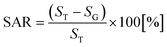 where SG is the geometric area (x × y), and ST is the topologic area (x × y × z). The elemental analysis was carried out with an energy-dispersive X-ray spectroscopy (EDS) system with the spectral mode (Thermo Fisher Noran System 7) under vacuum (over 2 × 10⁻⁴ Torr).
III. Results and discussion
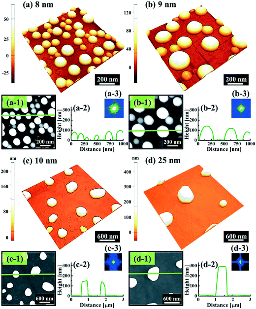
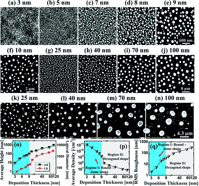
Fig. 1 and 2 show the evolution of self-assembled Au NPs by the variation of deposition amounts between 3 and 25 nm on 4H-SiC (0001). In general, at relatively low deposition amounts, round dome-shaped droplets (DPs) were fabricated and the size of the Au DPs was gradually expanded. With the increased deposition amounts, the dome-shaped DPs gradually evolved into larger hexagonal nano-crystals. Meanwhile, the density was significantly dropped. As is clearly shown in Fig. 1 and 2, self-assembled Au nanoparticles (3D islands) rather than films were fabricated at each deposition amount after annealing, which can be described based on the Volmer–Weber growth model. Given that the bonding energy between Au adatoms (EAu) is relatively stronger than that between Au adatoms and Si and C atoms (EI) (EAu > EI), the Au adatoms can spontaneously diffuse and form the nuclei at relatively low energy sites. With sufficient thermal energy at 800 °C, favorable diffusion can be expected and the Au nuclei can keep absorbing nearby adatoms with stronger bonding energy (EAu > EI) to form 3D islands until reaching an equilibrium, which can be similarly witnessed with Ag nanoparticles on SiC,26 and Au nanoparticles on MgB2.27 In the meantime, with the increased deposition amounts, additional Au atoms are available within the absorption boundary which in turn can result in the increased size of islands. Due to the merging tendency of larger islands, the density can be gradually reduced until a balance is reached in the thermodynamic system. More specifically, initially, with 3 nm Au deposition, small round dome-shaped DPs were fabricated with a highly packed density as shown in Fig. 1(a) and (a-2), and between 3 and 8 nm deposition amounts, a gradual size increase of the Au DPs with a sharp decrease in density was observed as is clearly shown in Fig. 1 and 2. At 9 nm, the shape of the Au NPs began to transform to polyhedral Au nano-crystals as evidenced by the slender facet formation on the AFM side-view in Fig. 2(b-1) and with additional depositions of 10 and 25 nm, the hexagonal shape much more evidently appeared as is clearly shown in Fig. 2(c) and (d). The self-assembled Au hexagonal nano-crystals on 4H-SiC (0001) with the Au deposition amounts of (a) 9.5, (b) 10 and (c) 25 nm can also be witnessed with the 3D side-view AFM images in Fig. S3.† The shape transformation of Au NPs can be guided by the underlying substrate crystal configuration depending on the growth conditions such that the final shape of the NPs under an equilibrium can balance the surface energy for a certain volume.28 Generally, when the surface energy is isotropic for a given volume, a spherical (dome) shape is preferred in order to minimize the surface energy. As the volume of nanostructures becomes larger and reaches the critical volume, the isotropic surface energy along various directions cannot be sustained, and the local breakage of the isotropy of the surface energy can lead to the formation of additional surfaces along the lower energy directions,23,28 such that, up to an 8 nm deposition amount, the resulting configuration was in the form of round dome shapes. However, above 9 nm, the Au NPs can absorb more Au adatoms with the increased deposition amount and the size increase by merging nearby droplets, and the surface energy of the Au NPs can become anisotropic, thus the resulting configuration can be hexagonal nano-crystals and truncation (or facet formation) can be obtained as is clearly seen in Fig. S3 and S4.† The surface morphology evolution of the Au NPs can also be witnessed with the Fourier filter transform (FFT) power spectra, as shown in Fig. 1(a-1)–(c-1) and 2(a-3)–(d-3). At 3 nm, a bright spot in the symmetric round shape occupied almost 90% of the area due to a broad distribution of droplet height. With the deposition amount increasing, the spot size drastically shrinks due to reduction in the height distribution and density reduction and finally becomes asymmetric because of the appearance of the polyhedron shape of Au nano-crystals. Fig. 3 shows the overall deposition amount variations between 3 and 100 nm, the evolution of self-assembled Au NPs on 4H-SiC (0001), and the summary of size, density and RRMS. The corresponding values are provided in Table S2.† Top-view and 3D side-view AFM images between 25 and 100 nm deposition amounts are provided in Fig. S5 and S6.† As discussed, above 9 nm, the formation of Au nano-crystals with clear facets occurred and kept evolving in larger crystals with the density reduction as shown in Fig. 3(e)–(j). In addition to the shape transition of the NPs, when the deposition amounts were systematically varied between 3 and 100 nm, the size of the Au nanostructures kept radically increasing by 105 times with the AH from ∼8.7 nm at 3 nm to ∼914.8 nm at 100 nm, and by 67 times with the LD from ∼45.6 to ∼3066.7 nm as a function of the deposition amount as shown in Fig. 3(o). The aspect ratio (AH![[thin space (1/6-em)]](https://www.rsc.org/images/entities/char_2009.gif) :LD) was ∼1:5 with 3 nm Au deposition and that with 100 nm Au deposition was ∼1:3, suggesting a preferential vertical growth. Correspondingly, the AD was rapidly decreased by ∼5 orders of magnitude from ∼1.18 × 10¹¹ to ∼7.6 × 106 cm−2 as a compensation of the size expansion as shown in Fig. 3(p). With the increased size of the NPs, RRMS was gradually increased from 2.1 to 304 nm between 3 and 100 nm as shown in Fig. 3(q). The elemental analyses of the corresponding samples are presented by the energy-dispersive X-ray spectroscopy (EDS) phase maps and spectra in Fig. 4. Fig. 4(a) shows the SEM image of the sample with 25 nm Au deposition and the combined phase map of Au and Si in Fig. 4(b) clearly matches with the SEM image. The separate maps of the Si and Au phases in Fig. 4(c) and (d) also clearly support the formation of Au NPs. The Au count line profiles and spectra on the locations with/without Au droplets are shown in Fig. 4(e)–(g), acquired from the lines and boxes in the inset of the SEM image. In Fig. 4(e), a high count of Au is clearly witnessed along the line profile (W) while only Si was observed with the profile (WO). Similarly, this is also observed with the existence of the Au Mα1 peak in the spectrum from the NP region in Fig. 4(f) while only Si Kα and C Kα are observed in Fig. 4(g). This clearly indicates that the fabrication of Au nanoparticles was based on the Volmer–Weber growth model without the formation of a wetting layer in between the Au NPs. The evolution of the Au Mα1 peak at 2.123 keV as a function of deposition amount is clearly observed in Fig. 4(h) from the deposition amounts variation from 3 to 100 nm, and the corresponding full range spectra are shown in Fig. S9.† For instance, the Au Mα1 count with 3 nm was ∼300 and gradually increased and reached ∼2400 with 100 nm. After the excitation of electrons to the N orbit, the electrons spontaneously release energy to relax to the M orbit, which results in the Mα1 peak, thus the increased deposition amount can directly enhance the count of the Au Mα1 peak. Fig. S7† presents the 3D side- and top-views of the EDS maps with 100 nm Au deposition and Fig. S8† shows the full range EDS spectra of the samples with (a) 3 and (b) 100 nm Au deposition amounts. In summary, the self-assembled Au NPs were successfully fabricated on 4H-SiC (0001) and the Au NPs very sensitively responded to the variation of the deposition amounts, which led to drastic evolution in the size and density, as well as the configuration being provided with EAu > EI.26,27 When the binding energy between adatoms is stronger, but not strong enough to maintain the 3D structure, the coalescence growth model can take dominance with the increased deposition amount, such that the layer formation of a Au film can follow immediately after a few nanometer depositions. For instance, Au NPs can be fabricated with less than 5 nm Au deposition on Si (111),29 glass,30 SiO2,31 and polymeric substrates (polystyrene and polymethylmethacrylate)32 but with further increased deposition amounts, the merging of Au nanostructures gradually occurred and they finally coalesced into
a layer based on the coalescence growth model. However, on SiC, the size of the self-assembled Au NPs was graduallyincreased with the facet formation even up to a 100 nm deposition amount. As another aspect, the Au NPs on 4H-SiC (0001) for a given deposition amount showed a relatively much smaller size distribution (i.e. at 3 nm, the AH is ∼8.7 nm and the LD is ∼45.6) with a highly packed density as compared with the counterparts on GaAs33–35 and Si,29,36 which can likely be due to the much higher diffusion barrier caused by the higher surface roughness of SiC.37
:LD) was ∼1:5 with 3 nm Au deposition and that with 100 nm Au deposition was ∼1:3, suggesting a preferential vertical growth. Correspondingly, the AD was rapidly decreased by ∼5 orders of magnitude from ∼1.18 × 10¹¹ to ∼7.6 × 106 cm−2 as a compensation of the size expansion as shown in Fig. 3(p). With the increased size of the NPs, RRMS was gradually increased from 2.1 to 304 nm between 3 and 100 nm as shown in Fig. 3(q). The elemental analyses of the corresponding samples are presented by the energy-dispersive X-ray spectroscopy (EDS) phase maps and spectra in Fig. 4. Fig. 4(a) shows the SEM image of the sample with 25 nm Au deposition and the combined phase map of Au and Si in Fig. 4(b) clearly matches with the SEM image. The separate maps of the Si and Au phases in Fig. 4(c) and (d) also clearly support the formation of Au NPs. The Au count line profiles and spectra on the locations with/without Au droplets are shown in Fig. 4(e)–(g), acquired from the lines and boxes in the inset of the SEM image. In Fig. 4(e), a high count of Au is clearly witnessed along the line profile (W) while only Si was observed with the profile (WO). Similarly, this is also observed with the existence of the Au Mα1 peak in the spectrum from the NP region in Fig. 4(f) while only Si Kα and C Kα are observed in Fig. 4(g). This clearly indicates that the fabrication of Au nanoparticles was based on the Volmer–Weber growth model without the formation of a wetting layer in between the Au NPs. The evolution of the Au Mα1 peak at 2.123 keV as a function of deposition amount is clearly observed in Fig. 4(h) from the deposition amounts variation from 3 to 100 nm, and the corresponding full range spectra are shown in Fig. S9.† For instance, the Au Mα1 count with 3 nm was ∼300 and gradually increased and reached ∼2400 with 100 nm. After the excitation of electrons to the N orbit, the electrons spontaneously release energy to relax to the M orbit, which results in the Mα1 peak, thus the increased deposition amount can directly enhance the count of the Au Mα1 peak. Fig. S7† presents the 3D side- and top-views of the EDS maps with 100 nm Au deposition and Fig. S8† shows the full range EDS spectra of the samples with (a) 3 and (b) 100 nm Au deposition amounts. In summary, the self-assembled Au NPs were successfully fabricated on 4H-SiC (0001) and the Au NPs very sensitively responded to the variation of the deposition amounts, which led to drastic evolution in the size and density, as well as the configuration being provided with EAu > EI.26,27 When the binding energy between adatoms is stronger, but not strong enough to maintain the 3D structure, the coalescence growth model can take dominance with the increased deposition amount, such that the layer formation of a Au film can follow immediately after a few nanometer depositions. For instance, Au NPs can be fabricated with less than 5 nm Au deposition on Si (111),29 glass,30 SiO2,31 and polymeric substrates (polystyrene and polymethylmethacrylate)32 but with further increased deposition amounts, the merging of Au nanostructures gradually occurred and they finally coalesced into
a layer based on the coalescence growth model. However, on SiC, the size of the self-assembled Au NPs was graduallyincreased with the facet formation even up to a 100 nm deposition amount. As another aspect, the Au NPs on 4H-SiC (0001) for a given deposition amount showed a relatively much smaller size distribution (i.e. at 3 nm, the AH is ∼8.7 nm and the LD is ∼45.6) with a highly packed density as compared with the counterparts on GaAs33–35 and Si,29,36 which can likely be due to the much higher diffusion barrier caused by the higher surface roughness of SiC.37
 |
| | Fig. 1 Self-assembled round dome-shaped Au droplets on 4H-SiC (0001) with a variation of Au deposition amounts between 3 and 7 nm. Au droplets were fabricated with a fixed annealing temperature of 800 °C and dwelling time of 450 s. (a)–(c) Atomic force microscopy (AFM) side-views of 1 × 1 μm2. (a-1)–(c-1) Two-dimensional (2D) Fourier filter transform (FFT) power spectra. (a-2)–(c-2) Corresponding AFM top-views of 1 × 1 μm2. (a-3)–(c-3) Corresponding cross-sectional line profiles. | |
 |
| | Fig. 2 Shape transition of the self-assembled Au nanoparticles on 4H-SiC (0001) by the variation of deposition amounts between 8 and 25 nm under identical growth conditions (800 °C, 450 s). AFM side-views of (a)–(b) 1 × 1 μm2 and (c)–(d) 3 × 3 μm2. AFM top-views of (a-1)–(b-1) 1 × 1 μm2 and (c-1)–(d-1) 3 × 3 μm2. (a-2)–(d-2) Cross-sectional line profiles acquired from the green lines drawn in (a-1)–(d-1). (a-3)–(b-3) 2D FFT power spectra. | |
 |
| | Fig. 3 Evolution of self-assembled Au nanostructures by the variation of deposition amounts between 3 and 100 nm on 4H-SiC (0001) annealed at 800 °C for 450 s. AFM top-views of (a)–(e) 3 × 3 μm2, (f) 10 × 10 μm2, and (g)–(j) 40 × 40 μm2. (k)–(n) SEM images of 21.5 (x) × 16.13 (y) μm2. (o)–(p) Plots of the average height (AH) and lateral diameter (LD), and average density (AD) of the Au NPs with error bars of ±5%. (q) Plot of the root mean squared roughness (RRMS) of the corresponding samples. | |
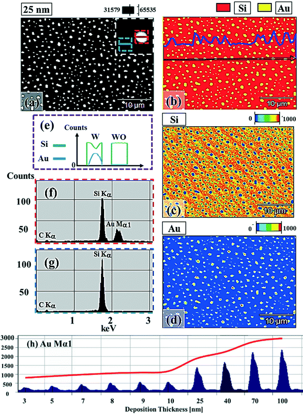 |
| | Fig. 4 Energy-dispersive X-ray spectroscopy (EDS) elemental characterization of the Au NPs. (a) Scanning electron microscopy (SEM) image of the sample with 25 nm thickness deposition. (b) EDS combined phase map of Si and Au. The line profile shows the Au component along the arrow. (c) Si phase map. (d) Au phase map. (e) EDS local line profiles of the element content of Si (green) and Au (blue), which are acquired from the lines with (W) and without (WO) the Au NPs marked with red (W) and blue (WO) lines in (a). (f)–(g) EDS spectra of the locations indicated with red (f) and blue (g) boxes. (h) Evolution of Au Mα1 peaks at 2.123 keV with the increased deposition amounts between 3 and 100 nm. | |
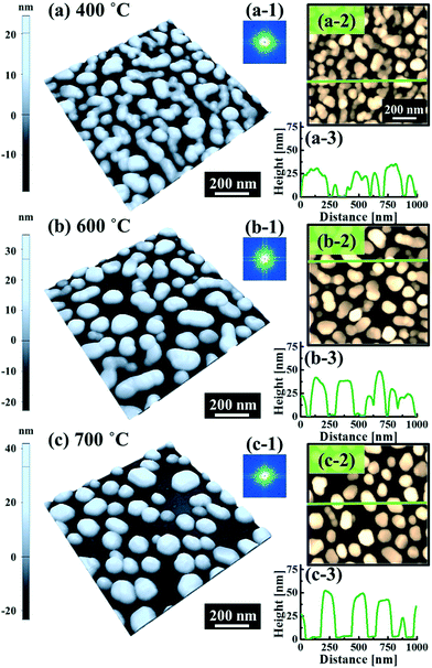
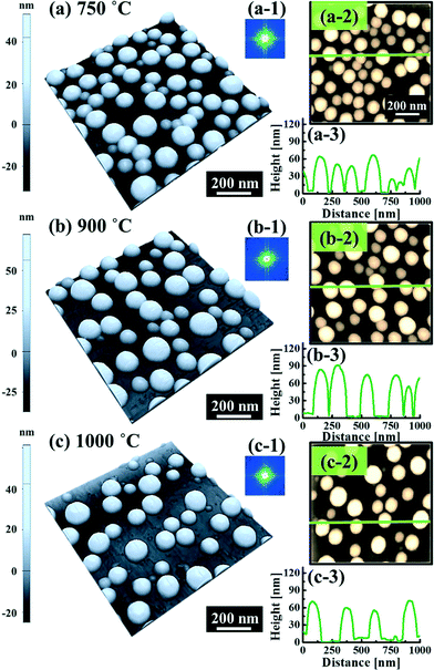
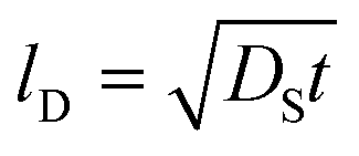
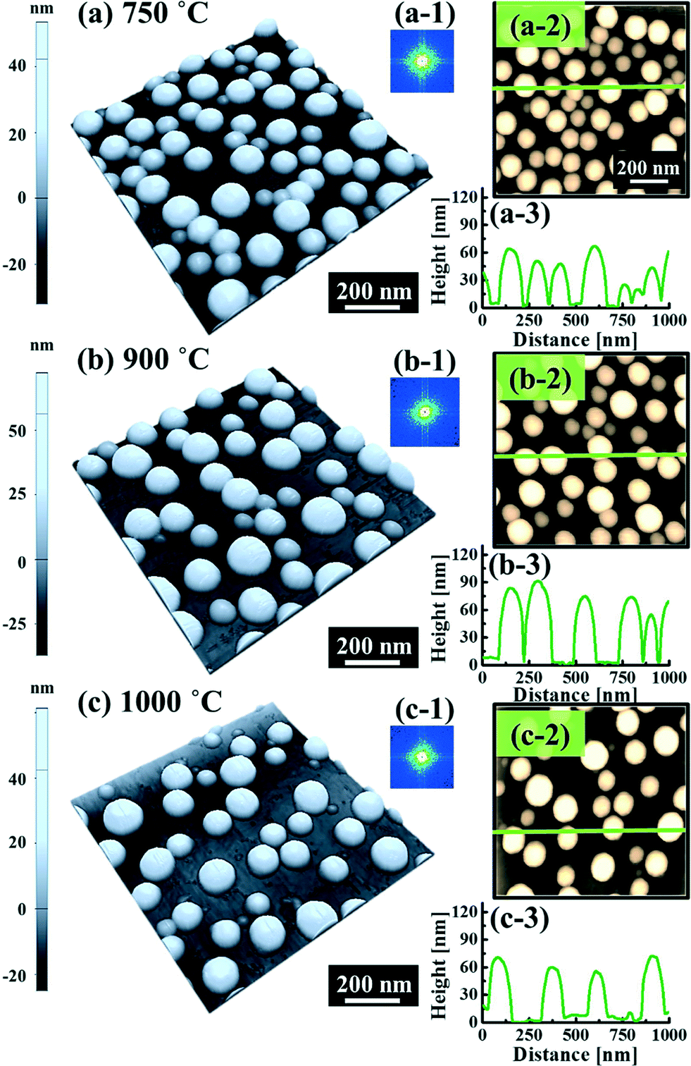
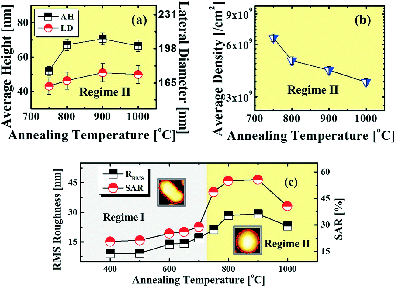
Fig. 5 and 6 show the configuration evolution of self-assembled Au nanostructures by the control of annealing temperatures between 400 and 1000 °C with a fixed deposition amount of 8 nm on 4H-SiC (0001). Generally, two distinctive configurations of Au nanostructures were observed with the systematic variation of annealing temperatures: Au nano-mounds between 400 and 700 °C (regime I) and round dome-shaped DPs between 750 and 1000 °C (regime II). A detailed evolution process of irregular Au nano-mounds with a smaller increment of annealing temperatures between 400 and 700 °C is shown with top- and side-view AFM images in Fig. S10–S11.† The formation of irregular Au nano-mounds can be described with the diffusion limited aggregation (DLA) growth model in conjunction with the thermodynamic diffusion theory.22,23 The diffusion length (lD) can be expressed as  , where DS is the surface diffusion coefficient and t is the residence time of Au atoms. Herein, DS can be given by
  and EA is the interface energy between Au and the substrate, and k is the Boltzmann constant.38 By combining both equations, the diffusion length (lD) can be expressed as a direct function of temperature such that the lD can be directly controlled by the variation of temperature. In the meantime, the vacancy of atoms in the Au film can occur at an elevated temperature, whose concentration can gradually increase along with the increased thermal energy. At a critical thermal energy or concentration of vacancy, it can turn into the formation of voids according to the DLA model.21,22,39 The voids can perforate the Au film and create punctures when the density of voids reaches a critical value, which gradually expands due to the enhanced Au adatom diffusion.40 Finally, the Au film branches into isolated Au mounds due to the Rayleigh instability41 which in turn results in the formation of isolated irregular Au mounds,22 such that, at 400 °C as is clearly seen in Fig. 5(a), the resulting geometry was connected Au wiggly branch structures with a height of ∼20 nm due to the limited diffusion. With the increased temperature up to 700 °C, the enhanced diffusion gradually led the separation of the Au wiggly structures into the isolated nano-mounds as described above which reached a height of ∼40 nm as is clearly shown in Fig. 5, S9 and S10.† The formation of irregular nano-mounds can also be observed with Co42 and Ni NPs.43 The morphological changes can also be described by the SAR and RRMS in Fig. 7(c) and both values in phase I were generally lower than those in phase II but were gradually increased along with the increased annealing temperature: 9–17 nm for RRMS and 20–30% for the SAR as shown in Fig. 7(c). As the AT was further increased to 750–1000 °C, self-assembled round dome-shaped Au droplets (DPs) were formed due to sufficient diffusion energy being provided with the stronger binding energy (EAu > EI) and generally, the size of the Au DPs was gradually increased while the density kept decreasing. The top-views and line profiles of the DPs are provided in Fig. 6 and S11.† The size and density are summarized in Fig. 7(a) and (b) and also specific values are listed in Table S3.† The enhanced diffusion can lead to an increased size of the DPs, and larger DPs with an increased absorption boundary tend to absorb or merge with nearby smaller DPs, thus the density decrease can occur until equilibrium is reached. For example, during the annealing temperature variations between 750 and 900 °C as shown in Fig. 7(a)–(b), the AH was increased by 1.4 times from 51.9 to 70.5 nm, and the LD was increased by 1.1 times from 161.9 to 174.8 nm, but the AD was decreased by 34.9% from 6.57 × 10⁹ to 4.28 × 109 cm−2. The size increase is also clearly observed in both the SAR and RRMS in Fig. 7(c). At 1000 °C, the size, SAR and RRMS of the DPs were sharply decreased, which can result from Au evaporation caused by the elevated temperature. As is well known, the melting point of the bulk of Au is 1064 °C, whereas the melting point of the Au NPs can be lower due to the variation of the Au vapor pressure saturation, as witnessed on MgO, SrTiO3, and Al2O3.44 In brief, along with the AT variation, the self-assembled Au nanostructures exhibited two distinctive configurations of irregular Au mounds (regime I) and round dome-shaped DPs (regime II). The irregular Au mounds were formed due to the diffusion limited aggregation at relatively low annealing temperatures between 400 and 700 °C, and between 750 and 900 °C, round dome-shaped DPs were fabricated due to the stronger binding energy (EAu > EI) and sufficient diffusion energy, and the size of the DPs was gradually increased while the density was decreased. The inverse relationship between the size and density of the DPs can also be observed on other substrates such as Si45,46 and sapphire.47
 |
| | Fig. 5 Evolution of Au nanostructures by the variation of annealing temperatures between 400 and 700 °C on 4H-SiC (0001). Each sample is fabricated with a fixed deposition amount of 8 nm and an annealing duration of 450 s. (a)–(c) AFM side-views of 1 × 1 μm2. (a-1)–(c-1) 2D FFT power spectra. (a-2)–(c-2) AFM top-views of 1 × 1 μm2. (a-3)–(c-3) Cross-sectional line profiles. | |
 |
| | Fig. 6 Fabrication of Au droplets with a variation of annealing temperatures between 750 and 1000 °C on 4H-SiC (0001) under fixed conditions (8 nm, 450 s). (a)–(c) AFM side-views of 1 × 1 μm2. (a-1)–(c-1) 2-D FFT power spectra. (a-2)–(c-2) AFM top-views of 1 × 1 μm2. (a-3)–(c-3) Cross-sectional line profiles. | |
 |
| | Fig. 7 (a)–(b) Plots of the AH, LD and AD with error bars of ±5%. (c) Plot of RRMS and the surface area ratio (SAR). The SAR is (β − α)/β × 100 (%), with a surface area (α) of x × y and a geometric area (β) of x × y × z. Insets: two AFM top-views in (c) are 150 × 150 nm2. | |
Fig. 8 shows a map of the self-assembled Au nanostructure fabrication with the variation of annealing temperature as a function of deposition amount. Depending on the fabrication conditions, the overall evolution is divided into three regimes: nano-mounds, droplets and nano-crystals. In the nano-mound regime, as indicated by No. 1 and 2, Au nanostructures nucleate but due to the low thermal energy or limited diffusion, the Au mounds were formed based on the diffusion limited aggregation model between 400 and 700 °C. In the droplet regime, as indicated by No. 3–6, due to the enhanced thermal energy, round dome-shaped Au droplets were fabricated above 750 °C, being provided with stronger binding energy (EAu > EI). In the nano-crystal regime, indicated by No. 7–10, self-assembled Au hexagonal nano-crystals were formed due to local breakage of the isotropy of the surface energy caused by the larger volume of the nanostructures, which occurred at ∼9 nm deposition. RRMS values of the related samples are shown in Fig. 8(a) and (b). Depending on the deposition amount, RRMS is gradually increased along with the size evolution of the nanostructures. Depending on the annealing temperature, RRMS is also gradually increased, however, from 900 °C, it is decreased potentially due to Au evaporation.
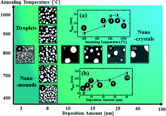 |
| | Fig. 8 Map of the fabrication of self-assembled Au nanostructures by the variation of the deposition amount versus annealing temperature. (a) RRMS of the samples synthesized with 8 nm Au deposition at various annealing temperatures. (b) RRMS of the samples with various deposition amounts annealed at 800 °C for 450 s. Insets: 1 × 1 μm2 for 1–7 and 3 × 3 μm2 for 8–10. | |
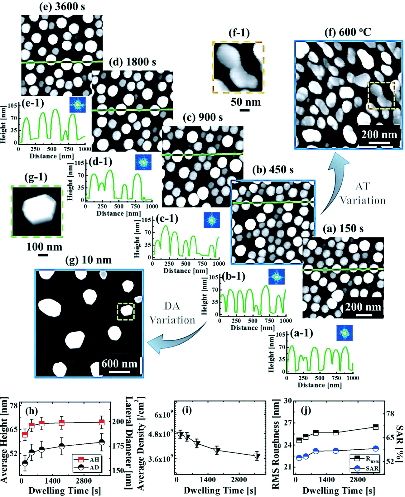
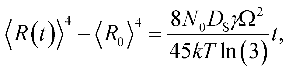
Fig. 9 shows the evolution of the self-assembled Au DPs by the variation of the dwelling time between 150 and 3600 s with 8 nm Au deposition at 800 °C. The 3D side-views are provided in Fig. S13.† As summarized in Fig. 9(h)–(i), the size of the self-assembled Au DPs gradually became larger with the increased dwelling time, while the density kept decreasing. The annealing duration related to the evolution of nanoparticles can be described based on Ostwald ripening,24 in which the average radius of the Au DPs (〈R(t)〉) can be expressed as 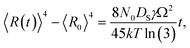 where 〈R0〉 is the initial radius of the Au DPs, and Ω is the atomic volume.25,38 The density of nucleation sites (N0) and the interface energy (γ) can be constant, thus the final size of the Au DPs (〈R〉) can be determined depending on the dwelling time variation, and based on the equation, 〈R〉 can be increased along with the increased dwelling time. For example, the LD was ∼157 nm with 150 s annealing and was increased to ∼180 nm with 3600 s, and similarly the AH of the DPs was 62.2 nm with 150 s annealing and was increased to 69 nm with 3600 s. Meanwhile the AD was 4.76 × 10⁹ per cm2 with 150 s which gradually decreased to 3.71 × 10⁹ per cm2 with 3600 s. Likewise, the SAR and RRMS also showed a gradual increase, as is shown in Fig. 9(j). The change of the size and density rather rapidly occurred at an earlier stage as is clearly seen with the sharper slopes of the plots up to 900 s, and as the time is further increased, the change became mild with the slender slope. With the increased annealing time, the critical size 〈RC〉 should be reached, and a naturally further increased time can only have an insignificant effect. In this experiment, relatively slow ramping (2 °C s−1) was utilized to ensure proper thermal conduction, thus the ripening could have occurred during ramping. The mild size and density change as compared to the temperature and deposition amount variation can also be observed with the similar FFT size and patterns. Nevertheless, it is worthwhile observing the size and density evolution of the DPs depending on the time. Meanwhile, as is shown in Fig. 9(f) and (g), the slight increase in deposition amount resulted in the formation of hexagonal Au nano-crystals and the small decrement of annealing temperature showed the fabrication of Au nano-mounds. In particular, we can conclude that the variation in dwelling time had nearly no effect on the shape of the Au NPs as the configuration was more strongly dependent on the annealing temperature and deposition amount for fixed conditions as discussed above.
 |
| | Fig. 9 Self-assembled Au droplets with the control of dwelling time between 150 and 3600 s with 8 nm Au deposition at 800 °C on 4H-SiC (0001). (a)–(e) AFM top-views of 1 × 1 μm2. (a-1)–(e-1) Cross-sectional line-profiles and 2D FFT power spectra. (f) and (f-1) Au nano-mounds fabricated at 600 °C with a constant deposition amount and dwelling time of 8 nm and 450 s. (g) and (g-1) Au nano-crystals fabricated with 10 nm Au deposition at a fixed annealing temperature and dwelling time of 800 °C for 450 s. (f) 1 × 1 μm2 and (f-1) 250 × 250 nm2. (g) 3 × 3 μm2 and (g-1) 500 × 500 nm2. (h) and (i) Plots of the AH, LD and AD with error bars of ±5%. (j) Plot of RRMS and the SAR. | |
IV. Conclusions
In summary, systematic approaches to control the size, density, and configuration of self-assembled Au nanostructures on 4H-SiC (0001) were investigated through the variation of deposition amount, annealing temperature and dwelling time. With the deposition amount variation, the self-assembled Au NPs of a round dome shape were successfully fabricated based on the Volmer–Weber growth model and evolved into hexagonal Au nano-crystals. Au NPs very sensitively responded to the deposition amount variation and resulted in a drastic size and density evolution along with the configuration transition. Depending on the annealing temperature variation, two distinctive configurations of Au nanostructures, Au nano-mounds (regime I) and round dome-shaped Au droplets (regime II), were fabricated based on the diffusion limited aggregation and thermodynamic theories. The dwelling time, size and density evolution of the dome-shaped Au droplets were discussed based on the Ostwald ripening theory.
Acknowledgements
Financial support from the National Research Foundation of Korea (no. 2011-0030079 and 2016R1A1A1A05005009), the National Science Foundation of USA (no. US/NSF/DMR1309989) and in part by the research grant of Kwangwoon University in 2016 are gratefully acknowledged.
References
- M. Valden, X. Lai and D. W. Goodman, Science, 1998, 281, 1647–1650 CrossRef CAS PubMed.
- M. J. Walsh, K. Yoshida, A. Kuwabara, M. L. Pay, P. L. Gai and E. D. Boyes, Nano Lett., 2012, 12, 2027–2031 CrossRef CAS PubMed.
- S.-S. Kim, Y.-R. Kim, T. D. Chung and B.-H. Sohn, Adv. Funct. Mater., 2014, 24, 2764–2771 CrossRef CAS.
- R. Kraya, L. Y. Kraya and D. A. Bonnell, Nano Lett., 2010, 10, 1224–1228 CrossRef CAS PubMed.
- T. Lohmuller, S. Triffo, G. P. O'Donoghue, Q. Xu, M. P. Coyle and J. T. Groves, Nano Lett., 2011, 11, 4912–4918 CrossRef CAS PubMed.
- P. Ginzburg, N. Berkovitch, A. Nevet and I. Shor, Nano Lett., 2011, 11, 2329–2333 CrossRef CAS PubMed.
- G. V. Naik, V. M. Shalaev and A. Boltasseva, Adv. Mater., 2013, 25, 3264–3294 CrossRef CAS PubMed.
- S. H. Mirsadeghi and J. F. Young, Nano Lett., 2014, 14, 5004–5009 CrossRef CAS PubMed.
- E. Thimsen, F. L. Formal, M. Gratzel and S. C. Warren, Nano Lett., 2011, 11, 35–43 CrossRef CAS PubMed.
- N. P. Dasgupta, J. Sun, C. Liu, S. Brittman, S. C. Andrews, J. Lim, H. Gao, R. Yan and P. Yang, Adv. Mater., 2014, 26, 2137–2184 CrossRef CAS PubMed.
- M. Kolíbal, T. Vystavěl, P. Varga and T. Šikola, Nano Lett., 2014, 14, 1756–1761 CrossRef PubMed.
- V. Schmidt, S. Senz and U. Golsele, Nano Lett., 2005, 5, 931–935 CrossRef CAS PubMed.
- L. J. D. Vreede, A. V. D. Berg and J. C. T. Eijkel, Nanopore Fabrication by Heating Au Particles on Ceramic Substrates, Nano Lett., 2015, 15, 727–731 CrossRef PubMed.
- T. James, Y. V. Kalinin, C.-C. Chan, J. S. Randhawa, M. Gaevski and D. H. Gracias, Voltage-Gated Ion Transport through Semiconducting Conical Nanopores Formed by Metal Nanoparticle-Assisted Plasma Etching, Nano Lett., 2012, 12, 3437–3442 CrossRef CAS PubMed.
- E. Velez-Fort, C. Mathieu, E. Pallecchi, M. Pigneur, M. G. Silly, R. Belkhou, M. Marangolo, A. Shukla and F. Sirotti, ASC Nano, 2012, 6, 10893–10900 CAS.
- H. Frenzel, A. Lajn, H. V. Wenckstern, M. Lorenz, F. Schein, Z. Zhang and M. Grundmann, Adv. Mater., 2010, 22, 5332–5349 CrossRef CAS PubMed.
- C. Huh, K.-H. Kim, B. K. Kim, W. Kim, H. Ko, C.-J. Choi and G. Y. Sung, Adv. Mater., 2010, 22, 5058–5062 CrossRef CAS PubMed.
- J. D. Caldwell, O. J. Glembocki, Y. Francescato, N. Sharac, V. Giannini, F. J. Bezares, J. P. Long, J. C. Owrutsky, I. Vurgaftman, J. G. Tischler, V. D. Wheeler, N. D. Bassim, L. M. Shirey, R. Kasica and S. A. Maier, Nano Lett., 2013, 13, 3690–3697 CrossRef CAS PubMed.
- T. Low and P. Avouris, ASC Nano, 2014, 6, 1086–1101 CrossRef PubMed.
- D. Tsivion and E. Joselevich, Nano Lett., 2013, 13, 5491–5496 CrossRef CAS PubMed.
- M.-Y. Li, Q. Zhang, P. Pandey, M. Sui, E.-S. Kim and J. Lee, Sci. Rep., 2015, 5, 13954 CrossRef PubMed.
- J.-Y. Kwon, T.-S. Yoon, K.-B. Kim and S.-H. Min, J. Appl. Phys., 2003, 93, 3270–3278 CrossRef CAS.
- T. A. Witten and L. M. Sander, Phys. Rev. B: Condens. Matter Mater. Phys., 1983, 27, 5686–5697 CrossRef.
- J. H. Yao, K. R. Elder, H. Guo and M. Grant, Phys. Rev. B: Condens. Matter Mater. Phys., 1993, 47, 14110–14125 CrossRef.
- F. Ruffino and M. G. Grimaldi, J. Appl. Phys., 2010, 107, 104321 CrossRef.
- F. Ruffino and M. G. Grimaldi, J. Appl. Phys., 2011, 110, 044311 CrossRef.
- A. V. Pogrebnyakov, J. M. Redwing, S. Raghavan, V. Vaithyanathan, D. G. Schlom, S. Y. Xu, Q. Li, D. A. Tenne, A. Soukiassian, X. X. Xi, M. D. Johannes, D. Kasinathan, W. E. Pickett, J. S. Wu and J. C. H. Spence, Phys. Rev. Lett., 2004, 93, 147006 CrossRef CAS PubMed.
- T. K. Sau and A. L. Rogach, Adv. Mater., 2010, 22, 1781–1804 CrossRef CAS PubMed.
- M.-Y. Li, M. Sui, E.-S. Kim and J. Lee, Cryst. Growth Des., 2014, 14, 1128–1134 CAS.
- D. Gaspar, A. C. Pimentel, T. Mateus, J. P. Leitao, J. Soares, B. P. Falcao, A. Araujo, A. Vicente, S. A. Filonovich, H. Aguas, R. Martins and I. Ferreira, Sci. Rep., 2013, 3, 1469 CAS.
- S. M. Tabakman, Z. Chen, H. S. Casalongue, H. Wang and H. Dai, Small, 2011, 7, 499–505 CrossRef CAS PubMed.
- F. Ruffino, V. Torrisi, G. Marletta and M. G. Grimaldi, Appl. Phys. A: Mater. Sci. Process., 2011, 103, 939–949 CrossRef CAS.
- M.-Y. Li, M. Sui, E.-S. Kim and J. Lee, Jpn. J. Appl. Phys., 2014, 53, 095502 CrossRef.
- S. Y. Sayed, B. Daly and J. M. Buriak, J. Phys. Chem. C, 2008, 112, 12291–12298 CAS.
- M. Sui, M.-Y. Li, E.-S. Kim and J. Lee, J. Appl. Crystallogr., 2014, 47, 1–6 CrossRef.
- L. K. Ono, F. Behafarid and B. R. Cuenya, ACS Nano, 2013, 7, 10327–10334 CrossRef CAS PubMed.
- M.-Y. Li, M. Sui, E.-S. Kim and J. Lee, J. Appl. Phys., 2014, 116, 084301 CrossRef.
- F. Ruffino, A. Canino, M. G. Grimaldi, F. Giannazzo, C. Bongiorno, F. Roccaforte and V. Raineri, J. Appl. Phys., 2007, 101, 064306 CrossRef.
- W. Lu and K. Komvopoulos, J. Appl. Phys., 2000, 76, 3206–3208 CAS.
- F. Ruffino and M. G. Grimaldi, Thin Solid Films, 2013, 536, 99–110 CrossRef CAS.
- A. M. Glaeser, Interface Sci., 2001, 9, 65–82 CrossRef CAS.
- J. Lian, L. Wang, X. Sun, Q. Yu and R. C. Ewing, Nano Lett., 2006, 6, 1047–1052 CrossRef CAS.
- L. Kondic, Phys. Rev. E: Stat., Nonlinear, Soft Matter Phys., 2009, 79, 026302 CrossRef PubMed.
- G. Meng, T. Yanagida, M. Kanai, M. Suzuki, K. Nagashima, B. Xu and F. Zhuge, Phys. Rev. E: Stat., Nonlinear, Soft Matter Phys., 2013, 87, 012405 CrossRef PubMed.
- M. Sui, M.-Y. Li, E.-S. Kim and J. Lee, Nanoscale Res. Lett., 2013, 8, 525 CrossRef PubMed.
- F. Ruffino, A. Canino, M. G. Grimaldi, F. Giannazzo, F. Roccaforte and V. Raineri, J. Appl. Phys., 2008, 104, 024310 CrossRef.
- C.-Y. Chen, J.-Y. Wang, F.-J. Tsai, Y.-C. Lu, Y.-W. Kiang and C. C. Yang, Opt. Express, 2009, 17, 14186 CrossRef CAS PubMed.
Footnote |
| † Electronic supplementary information (ESI) available. See DOI: 10.1039/c5ce02439k |
|
| This journal is © The Royal Society of Chemistry 2016 |
Click here to see how this site uses Cookies. View our privacy policy here. 
 Open Access Article
 This Open Access Article is licensed under a Creative Commons Attribution-Non Commercial 3.0 Unported Licence
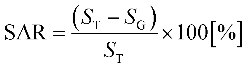 where SG is the geometric area (x × y), and ST is the topologic area (x × y × z). The elemental analysis was carried out with an energy-dispersive X-ray spectroscopy (EDS) system with the spectral mode (Thermo Fisher Noran System 7) under vacuum (over 2 × 10⁻⁴ Torr).
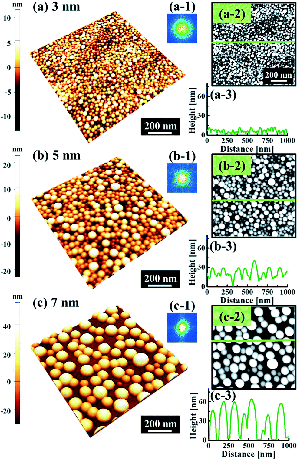


 , where DS is the surface diffusion coefficient and t is the residence time of Au atoms. Herein, DS can be given by
 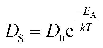 and EA is the interface energy between Au and the substrate, and k is the Boltzmann constant.38 By combining both equations, the diffusion length (lD) can be expressed as a direct function of temperature such that the lD can be directly controlled by the variation of temperature. In the meantime, the vacancy of atoms in the Au film can occur at an elevated temperature, whose concentration can gradually increase along with the increased thermal energy. At a critical thermal energy or concentration of vacancy, it can turn into the formation of voids according to the DLA model.21,22,39 The voids can perforate the Au film and create punctures when the density of voids reaches a critical value, which gradually expands due to the enhanced Au adatom diffusion.40 Finally, the Au film branches into isolated Au mounds due to the Rayleigh instability41 which in turn results in the formation of isolated irregular Au mounds,22 such that, at 400 °C as is clearly seen in Fig. 5(a), the resulting geometry was connected Au wiggly branch structures with a height of ∼20 nm due to the limited diffusion. With the increased temperature up to 700 °C, the enhanced diffusion gradually led the separation of the Au wiggly structures into the isolated nano-mounds as described above which reached a height of ∼40 nm as is clearly shown in Fig. 5, S9 and S10.† The formation of irregular nano-mounds can also be observed with Co42 and Ni NPs.43 The morphological changes can also be described by the SAR and RRMS in Fig. 7(c) and both values in phase I were generally lower than those in phase II but were gradually increased along with the increased annealing temperature: 9–17 nm for RRMS and 20–30% for the SAR as shown in Fig. 7(c). As the AT was further increased to 750–1000 °C, self-assembled round dome-shaped Au droplets (DPs) were formed due to sufficient diffusion energy being provided with the stronger binding energy (EAu > EI) and generally, the size of the Au DPs was gradually increased while the density kept decreasing. The top-views and line profiles of the DPs are provided in Fig. 6 and S11.† The size and density are summarized in Fig. 7(a) and (b) and also specific values are listed in Table S3.† The enhanced diffusion can lead to an increased size of the DPs, and larger DPs with an increased absorption boundary tend to absorb or merge with nearby smaller DPs, thus the density decrease can occur until equilibrium is reached. For example, during the annealing temperature variations between 750 and 900 °C as shown in Fig. 7(a)–(b), the AH was increased by 1.4 times from 51.9 to 70.5 nm, and the LD was increased by 1.1 times from 161.9 to 174.8 nm, but the AD was decreased by 34.9% from 6.57 × 10⁹ to 4.28 × 109 cm−2. The size increase is also clearly observed in both the SAR and RRMS in Fig. 7(c). At 1000 °C, the size, SAR and RRMS of the DPs were sharply decreased, which can result from Au evaporation caused by the elevated temperature. As is well known, the melting point of the bulk of Au is 1064 °C, whereas the melting point of the Au NPs can be lower due to the variation of the Au vapor pressure saturation, as witnessed on MgO, SrTiO3, and Al2O3.44 In brief, along with the AT variation, the self-assembled Au nanostructures exhibited two distinctive configurations of irregular Au mounds (regime I) and round dome-shaped DPs (regime II). The irregular Au mounds were formed due to the diffusion limited aggregation at relatively low annealing temperatures between 400 and 700 °C, and between 750 and 900 °C, round dome-shaped DPs were fabricated due to the stronger binding energy (EAu > EI) and sufficient diffusion energy, and the size of the DPs was gradually increased while the density was decreased. The inverse relationship between the size and density of the DPs can also be observed on other substrates such as Si45,46 and sapphire.47
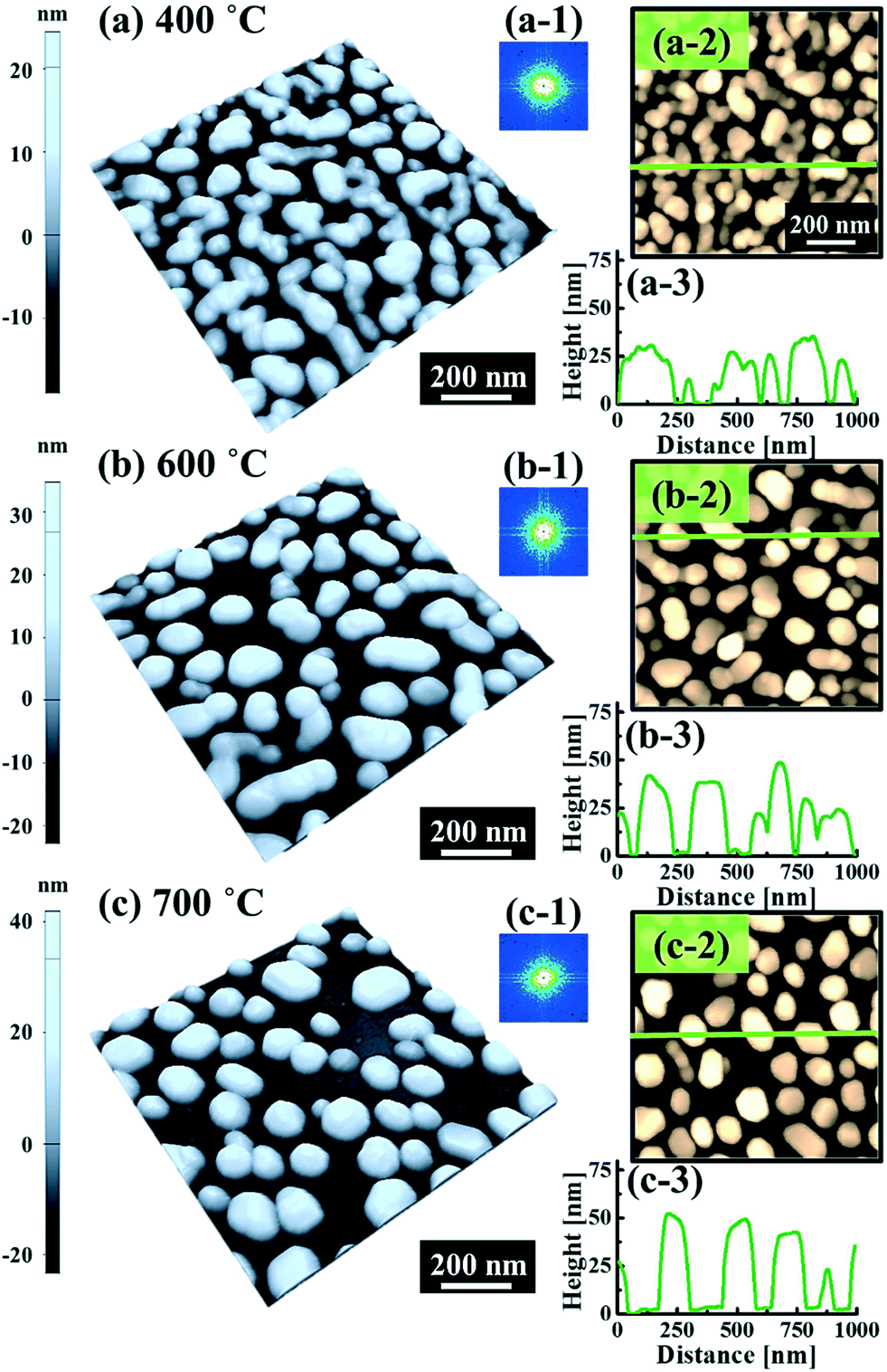

 where 〈R0〉 is the initial radius of the Au DPs, and Ω is the atomic volume.25,38 The density of nucleation sites (N0) and the interface energy (γ) can be constant, thus the final size of the Au DPs (〈R〉) can be determined depending on the dwelling time variation, and based on the equation, 〈R〉 can be increased along with the increased dwelling time. For example, the LD was ∼157 nm with 150 s annealing and was increased to ∼180 nm with 3600 s, and similarly the AH of the DPs was 62.2 nm with 150 s annealing and was increased to 69 nm with 3600 s. Meanwhile the AD was 4.76 × 10⁹ per cm2 with 150 s which gradually decreased to 3.71 × 10⁹ per cm2 with 3600 s. Likewise, the SAR and RRMS also showed a gradual increase, as is shown in Fig. 9(j). The change of the size and density rather rapidly occurred at an earlier stage as is clearly seen with the sharper slopes of the plots up to 900 s, and as the time is further increased, the change became mild with the slender slope. With the increased annealing time, the critical size 〈RC〉 should be reached, and a naturally further increased time can only have an insignificant effect. In this experiment, relatively slow ramping (2 °C s−1) was utilized to ensure proper thermal conduction, thus the ripening could have occurred during ramping. The mild size and density change as compared to the temperature and deposition amount variation can also be observed with the similar FFT size and patterns. Nevertheless, it is worthwhile observing the size and density evolution of the DPs depending on the time. Meanwhile, as is shown in Fig. 9(f) and (g), the slight increase in deposition amount resulted in the formation of hexagonal Au nano-crystals and the small decrement of annealing temperature showed the fabrication of Au nano-mounds. In particular, we can conclude that the variation in dwelling time had nearly no effect on the shape of the Au NPs as the configuration was more strongly dependent on the annealing temperature and deposition amount for fixed conditions as discussed above.