
Mapping minimum reflection distribution of surface plasmon resonance with a complex refractive index†
Xin
Hong
*a,
Marta C.
Lapsley
b,
Yunjing
Shang
a and
Elizabeth A. H.
Hall
 *b
*b
aDepartment of Biomedical Engineering, Faculty of Electronic Information and Electrical Engineering, Dalian University of Technology, 116024, China. E-mail: hongxin@dlut.edu.cn; yjshang@dlut.edu.cn
bInstitute of Biotechnology, Department of Chemical Engineering and Biotechnology, University of Cambridge, Tennis Court Road, Cambridge, CB2 1QT, UK. E-mail: lisa.hall@biotech.cam.ac.uk; m.lapsley@cetnet.co.uk
First published on 4th November 2016
Abstract
One of the main challenges in making any further advances in the field of SPR biosensing is in the detection of small molecules, low analyte concentrations, and single particle interactions. To this end, labels have been used to amplify the signal of this traditional label-free technique. The physical properties associated with these labels can enhance the SPR signal by affecting the dielectric constant both in the real and imaginary parts. In this paper, we have taken a holistic approach to considering the dielectric properties of these labels and their effect on the minimum resonance intensity (MI) is mapped for the Kretschmann SPR configuration. These maps provide a way for matching label properties for particular SPR conditions and reveal that thicker Au films (∼65 nm) make the MI method more suitable for the detection of absorbing materials. Whereas the wavelength SPR at 50 nm Au film thickness generates a shift of similar or lower magnitude for adsorption of the absorbing label, compared with BSA adsorption, in the ‘thick’-film SPR using the MI format, the signal due to the non-absorbing BSA adsorption tends towards zero (background), whereas the absorbing label produces a large well resolved signal.
Introduction
Surface plasmon resonance (SPR) as a robust analysis tool has been broadly used in the measurement of biological or chemical interactions, due to its high sensitivity, ability for label free sensing, real time kinetic measurements, and the vast array of capture ligands compatible with the sensor surface.1 The unique label-free character benefits the measurements without needing to alter the molecule chemically by labelling. However, this ability is challenged when measurements are required for the detection of small molecules, low analyte concentrations or single molecule interactions. It is well established that SPR supported on a thin metal film, typically gold, has an exponentially decaying electric field penetration into a thin layer of dielectric next to the gold surface of ∼150 nm at optical frequencies, and is referred to as the sensing layer.2 Perturbation of the complex refractive index within this sensing layer alters the SPR conditions allowing for detection of analytes at the sensor surface. In the cases of small molecule detection, the refractive index variation within the sensing evanescent field is far less than the sensor's sensitivity.3 Thus, to meet the sensitivity requirements, labels are employed to help enhance the sensing properties.The introduction of labels can for example amplify the signal by mass increase. Examples of this strategy include labelling with proteins4,5 and non-metallic nanoparticles,6 and the use of a sandwich assay format.7 The larger entity of the label increases the perturbation in the real part of the refractive index in the sensing layer, thus causing the signal amplification. However, at the same time if the label is too large, its steric hindrance and other surface occlusions increase the possibility of altering reaction kinetics or protein function as well.8 In this respect, nano-labels might be expected to show less perturbation, but might also provide lower signal amplification.
Thus, compared with these labels, plasmonic metal nano-particles, mostly taken as gold, are rather interesting, since they amplify the signal by a more complicated mechanism. The particles provide “nano-platforms” on which many molecules can assemble. When more “nano-platforms” go into the detection area, not only does the large mass cause the signal enhancement, but also the plasmonic coupling between the particles and the thin gold film contributes a prominent amplification to the signal. However, it should be noted that the signal enhancement caused by coupling is rather complex and varies with the distance between the particle and the film.9 Even though the resonant wavelength of a single gold nanoparticle shows a sharp red shift when it approaches much closer to the interface, the SPR at the interface is hardly influenced by it.10 With the increase of the particle number, more particle dipoles are coupled to their image field inside the gold layer, which modifies both fields. Introduction of the metallic nanoparticles causes a large SPR wavelength shift which is reported to enhance the sensitivity in the pM range.11 While attention may be focussed on the peak SPR wavelength shift or on fixed wavelength SPR, the resonance angle shift, we have shown that the classical SPR format can provide a starting point for more sensitive solutions. As previously reported, using a theoretical design process employing evolutionary algorithms (EAs), an emergent population of possible solutions may arise which deviate from the classical SPR Au film thickness of ∼50 nm and propose measurements that are based on the angle, wavelength or phase.12
However, one physical property, minimum reflectance on the SPR curve, is generally ignored. The occurrence of SPR is well characterized as a dip in the distribution curve of reflection vs. angle (or wavelength). The property determining the minimum reflectance (denoted as MI in this paper) is associated with labels that have an absorbing character. The absorbing imaginary part of the refractive index not only broadens the resonance peak but also varies the MI.13 Besides metallic nanoparticles, the absorbing properties can also come from some other big families of compounds, such as dye molecules or artificial fluorescent proteins, and the practice of using these compounds as SPR labels is being paid more attention.14–16 Nevertheless, the combination of a MI detection method with these absorbing labels has been less explored. However, this combination has the following potential: (1) it can be designed to overwhelm the non-absorbing baseline; (2) the optical properties associated with these absorbing labels can make the measurement window tuneable to avoid background disturbance; (3) the variations in the intensity produce opportunities for SPR imaging and can reduce the component requirements for the devices compared with angular or wavelength SPR. To this end, an understanding of the MI distribution with the absorbing label's physical properties is necessary to optimize the detection by selection of the right labels. In this paper, based on the typical Kretschmann structure we generalize a map, which shows the MI distribution with the complex refractive index. Like our previous output from a simple genetic algorithm, where isosurfaces with the theoretically enhanced response guide the design of the SPR format and label/indicator properties, the map provides an intuitionist method to select the physical properties. As for our previous non-classical SPR designs, we show that 50 nm, the thickness of the gold film normally found for the best sensitivity in the wavelength or angular SPR method, is the worst for MI detection. When the film is thicker, the sensitivity can be four times that at 50 nm. Furthermore, in the detection of absorbing materials, the MI method is even more sensitive on these thicker Au-film sensing chips. The impact of absorbing dye molecules as potential SPR labels in the MI measurement was used here as a model for numerical calculation and experimental examination.
Numerical calculations
In Kretschmann's structure, light is coupled by a prism to match the momentum conservation condition with the surface plasmon at the interface of glass/gold. Absorbing labels produce the third enhancement layer with a complex dielectric constant on the metal surface. Phosphate buffer solution is used to provide and simulate a typical environment for biological measurement. In this glass/metal/enhancement layer/water structure, the optical properties of each layer are described as dielectric constant εj, permeability μj and thickness hj. The transverse magnetic (TM) white light illuminates the glass/gold interface with the specific angle to excite SPR after being coupled by the prism. At each interface, the light goes through transmission and reflection, which is based on Fresnel coefficients. Hansen17 derived explicit formulas for the mean-square electric fields induced by electromagnetic radiation in a N-phase stratified medium, which built a foundation to trace the reflection and transmission layer by layer. The tangential fields at the first boundary are related to the final boundary which were numerically calculated by the following equation, | (1) |

 ,
,  .
.
The derived reflection coefficient of the parallel polarization is as follows:
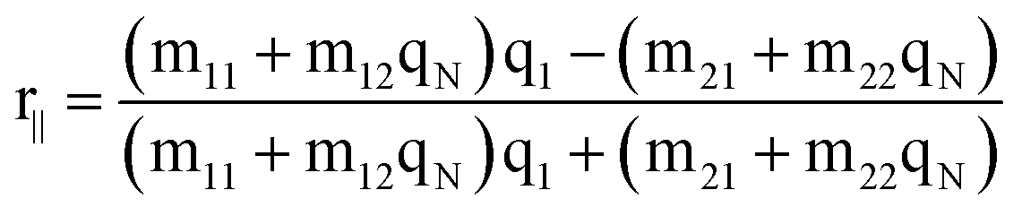
The reflectance is R∥=|r∥|2.
In the calculations presented here, the incident angle θ1 is set to be 72° which is within the range of allowed angles for SPR coupling. The thickness of the sensing layer (i.e. the absorbing layer or label layer) was set to be 1.5 nm, and the thickness of the gold layer was set as specified with each result. The reflectance curves were recorded with respect to wavelength and a Lorenz fit was applied to locate the minimum and its reflection value. The real and imaginary parts of the refractive index were varied to create the MI maps.
Materials and method
Bovine serum albumin (BSA), phosphate buffer and fluorescent red 635 maleimide (λex = 640 nm ± 5 nm) were purchased from Sigma-Aldrich. Unless otherwise stated, all solutions were prepared with ultra-pure MilliQ water (resistance > 18 MΩ).A home built spectral SPR setup was used for the measurements whose details were described elsewhere.9 The experimental procedure is as follows. After washing with ultra-high pure water (UHP), phosphate buffer was injected into the flow cell to obtain a base line. Then 1 mg ml−1 BSA in buffer solution was injected and allowed to run for ∼30 minutes to adsorb onto the Au chips and provide a matrix for the attachment of FR635 dye molecules. BSA in the bulk solution was removed by washing with phosphate buffer after which 2 μg ml−1 FR635 in buffer solution was injected into the flow cell. The assimilation of FR635 was detected by both shifts in the resonance wavelength and changes in the peak absorption.
Results and discussion
Map of the MI distribution
The MI distribution with both the real and imaginary parts of the complex refractive index is mapped as shown in Fig. 1(a) for a gold layer of thickness 60 nm. The x and y axes are the real and imaginary parts of the complex refractive index respectively. In the map, the colour of each point located at (x, y) illustrates the MI value when the enhancement layer's refractive index is set as x + iy. The value scale is shown in the colour bar. In the red areas of the map, MI tends to be 1.0, which indicates that no SPR can be excited. Thus, the dyes whose refractive index is in these areas are not suitable to be SPR labels. In contrast, in the blue areas of the map, MI tends to the value of 0, which is associated with sharp SPR curves. Two axes of x = 0 and y = 0 separate the map into 4 quadrants labelled as I–IV. In the first quadrant, the real and imaginary parts of the refractive index are both positive. These values are associated with many common absorbing materials, whose absorbing properties cause energy loss when light interacts with them. In the fourth quadrant, the negative imaginary part can cause an amplification of light which is often associated with materials providing the gain medium of lasers. The second and the third quadrant have negative real parts; this might include the properties of artificial nanostructures, for example metamaterials. However, for these materials, permeability μ is no longer 1. So, it should be noted that these two quadrants in the map cannot be equated with those structures. | ||
| Fig. 1 MI map and the SPR curves in specific areas pointed by arrows A–C. (a) The MI map for the gold film of thickness 60 nm. The map was calculated based on the wavelength SPR method. Maps from the angular SPR method were also calculated (see ESI†). (b)–(d) The SPR curves pointed by the arrows A, B, and C on the map in (a). | ||
In the map, it can be seen that there is a line at y = 0, across which a small variation in the imaginary part can cause an obvious colour change. In contrast, no obvious change is illustrated along the line (i.e. with change in the value of x), which indicates that the MI method is not sensitive to the non-absorbing materials. Several interesting colour borders are identified by the direction of arrows A–C and the corresponding SPR curves are shown in Fig. 1(b)–(d). Along arrow A, the SPR follows the passage from water, with the refractive index of 1.333, providing the background curve as shown in blue (Fig. 1(b)), and then the addition of an absorbing material, causing an increase in the imaginary part, which not only broadens the curve but also raises the MI. This property points to a format that is rather insensitive to layers of non-adsorbing materials (increase in the value of x) on the surface, but which “switches on” the signal by labelling absorbing materials (increase in the value of y). Arrow B follows a similar trend, but moves from a higher to a lower area of MI.
Another interesting area is pointed out by arrow C. When the imaginary part is kept constant, the changes caused in the real part of the refractive index increase the MI shown in Fig. 1(d), but cause almost no change in wavelength. This characteristic suggests applications where the surface is first modified by an absorbing layer, whose function is to act as an amplifier for non-absorbing overlayers. So, the addition of analytes will switch on the ΔMI signal by a contribution to the real part of the refractive index. Attention should however be paid to the sharp movement in the red area of the map from this area, since no SPR occurs, as shown by the blue curve in Fig. 1(d).
Based on the above discussion, there are opportunities to use these properties either by adopting an adsorbing material as a label, or by modifying the base Au SPR surface with an absorbing overlying film and then detecting the binding of non-adsorbing analytes on top of that modified surface. In both cases, the areas close to the axes of x = 0 and y = 0 are of most interest. Many perturbations added around the axes will cause the MI colour change between dark and light blue. It is rather obvious to deduce that if the dark blue band is narrower, the detection sensitivity can be higher. To explore this, we expanded the calculation further, by varying the thickness of the gold film since the evanescent field drops exponentially within it.
Thicker films sharpen the areas
The MI distributions for gold film thickness from 30–70 nm are shown in Fig. 2. There is a clear boundary line close to y = 0. But at 50 nm (and to a lesser extent 40 nm), y = 0 lies in the middle of a dark blue zone so no obvious change can be noticed in MI with the increase or decrease in the imaginary part of the refractive index. This is especially interesting since it is the normal thickness for classical SPR. So, contrary to the normal format for the wavelength or angular SPR method, the map in Fig. 2(c) indicates that the 50 nm Au thickness is the worst thickness to be used in monitoring MI change due to an absorbing label. With Au thickness increase, the colour bands narrow towards the centre and the axes. When the thickness is more than 50 nm, the maps change into “windmill” shapes and sharpen the borders. This phenomenon suggests potential for improved sensitivity using this method and it can be seen that at 70 nm Au, in quadrant I, changes similar to those indicated by arrows A and C in Fig. 1(a) cause a bigger change in MI for a smaller perturbation in the imaginary or real part of the refractive index.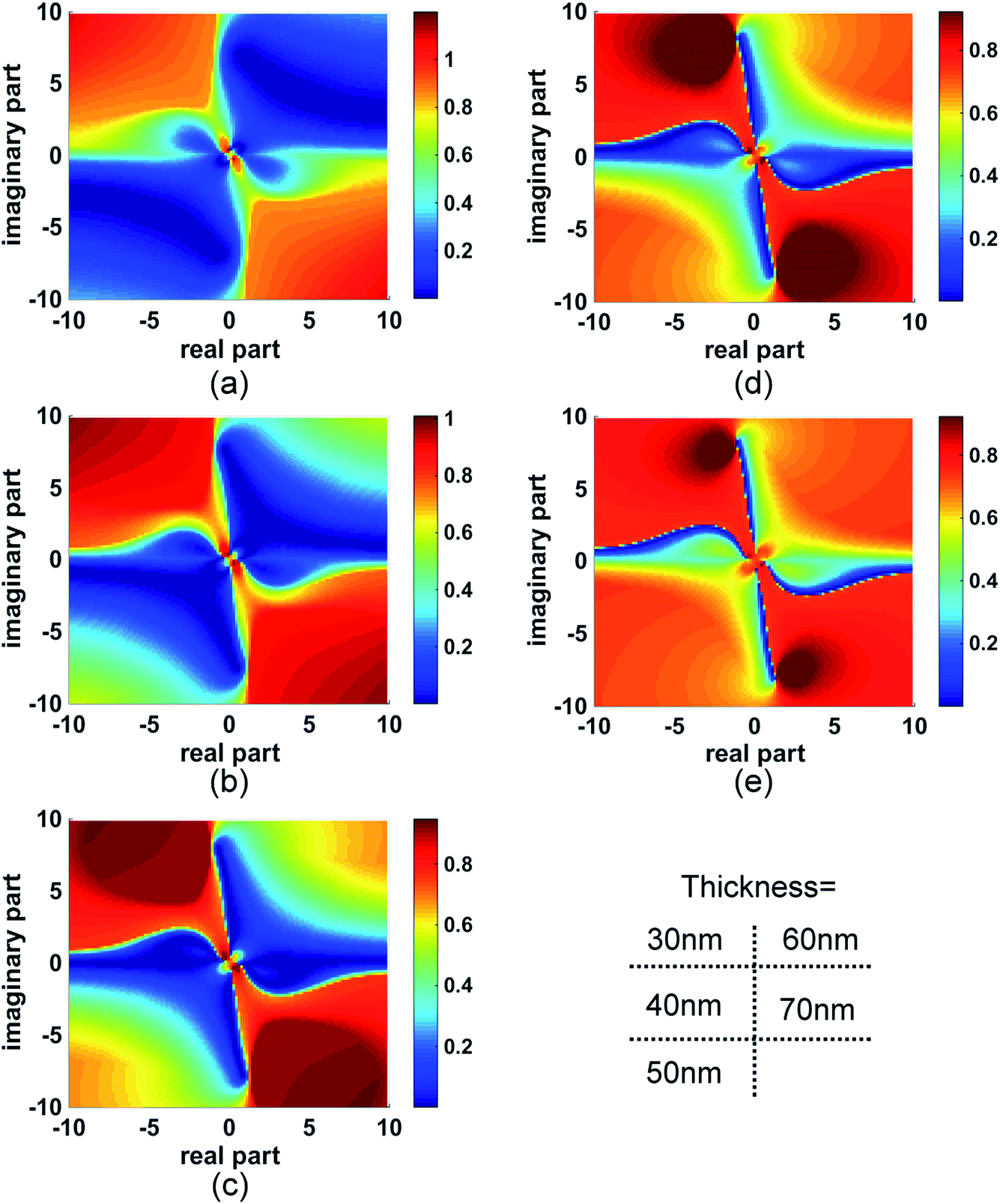 | ||
| Fig. 2 The MI distribution mapped with the complex refractive index at different thicknesses of gold films. In the map the x axis and y axes are respectively the real part and the imaginary part of the complex refractive index of the enhancement layer on the gold film, and at each point the colour shows MI extracted from the SPR curves. (a)–(e) The thickness of the gold film is 30 nm, 40 nm, 50 nm, 60 nm and 70 nm, respectively. | ||
Experimental testing of fluorescent red FR635 as the absorbing label
A wavelength SPR setup was employed with the aim to provide an easy matching of the optical band to the absorbing properties of the dye, simply by setting the right incident angle. In this experiment, fluorescent red FR635 with extinction peak wavelength λex = 640 nm ± 5 nm was chosen as the absorbing label. With the incident angle being set at 72 degrees, the SPR excitation wavelength is ∼632 nm. The binding between BSA (a non-absorbing material) and FR635 (an absorbing material) was measured and recorded by monitoring both wavelength and MI shifts at the same time, as shown in Fig. 3. In this figure, the same interaction was measured on SPR chips with different thicknesses of the gold film. The first layer used was BSA and adsorption to the Au layer was followed; this was followed by FR635 labelling. As shown in Fig. 3, after washing with ultra-high pure water, phosphate buffer was injected to get a baseline and then BSA and Fr635 were deposited. The peak extinction shown in Fig. 3 was extracted from a real-time optical density (OD) measurement (see ESI†). As suggested by Fig. 1(b)–(d), for the SPR reflection curve, the MI associated with the extinction peak (1.0-MI) provides a considerably enhanced measurement of the adsorbing compound, but is rather insensitive to the non-adsorbing BSA.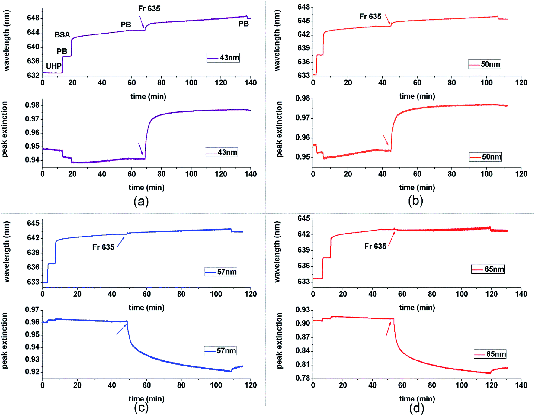 | ||
| Fig. 3 Experimental results of the simultaneous monitoring by peak extinction (1-MI) and wavelength SPR methods. Samples using different thicknesses of the gold film (a–d) were used. Each step seen in the wavelength plot corresponds to the injection of pure water, phosphate buffer, BSA and Fr635 respectively (see labelling for the wavelength plot in (a)). The corresponding sequence of steps is overlaid on the peak extinction plots, but some of the steps for non-absorbing compounds are not distinguishable in these plots at some thicknesses. The arrow in each curve indicates the injection of Fr635. (a)–(d) The same measurement carried out with the thickness of the gold film as ∼43 nm,∼50 nm,∼57 nm and ∼65 nm. | ||
At the thickness < 50 nm Au, the presence of absorbing FR635 causes a positive shift in MI while at the thickness > 50 nm, the MI makes a reverse shift in response to the addition of FR635. This result agrees well with the theoretical curves as shown in Fig. 2 and the earlier discussion. The colour changes from light to dark blue at thickness = 40 nm in the heat map (Fig. 2) while at the thickness of 60 nm or 70 nm (Fig. 1 and 2) the colour changes from dark to light. The thickness of ∼50 nm is the turning point boundary where the MI change shifts to the opposite direction. Thus, at this turning point the change in MI is potentially smaller. However, it should be noted that in all these films (even at 50 nm) the MI method shows a rather large relative shift in the presence of the absorbing material, compared with the non-absorbing material, bovine serum albumin (BSA). This selection and amplification of the signal due the absorbing material can be a highly desirable feature for design of a biosensor platform. Furthermore, contrary to the proposed MI method, it is not surprising to see that the wavelength method loses its detection ability as the thickness moves away from the optimum 50 nm, as seen in (c) and (d) for ∼57 nm and ∼65 nm. The data comparison in Fig. 3 therefore indicates that the MI method may be more suitable for the detection of absorbing materials, since (1) it is more tolerant to the Au thickness of the sensor chips; (2) it provides a rather large relative shift which can give a better signal to noise ratio against the non-absorbing background.
To further explore the detection format, we come back to comparing Fig. 3 with the experimental outcome. The addition of absorbing FR635 solution caused ∼2 nm wavelength shift and ∼0.02 absorption shift at 50 nm Au. To remove ambiguity caused by the difference in the units, the respective binding curves were examined and the kinetic coefficient was used to make a comparison (see ESI†). Kinetic measurements are a typical outcome of SPR experiments, so that their comparison using these different SPR formats provides further insight into the measurement potential. Since interaction with the surface can exhibit a change in the SPR wavelength, angle, phase or MI shift, the sensorgram from each of these parameters should hold the information of association and dissociation constants Ka and Kd. KD (which is the ratio between Ka and Kd) is usually used to evaluate the equilibrium status. This kinetic coefficient is supposed to be independent of the measurement method when it is optimised. Based on the sensorgrams, a non-linear least square fitting was used to obtain KD for the dynamic interaction model.18 The fitting result is shown in Table 1.
| Method | Wavelength thickness = 50 nm | MI thickness = 43 nm | MI thickness = 50 nm | MI thickness = 57 nm | MI thickness = 65 nm |
| K D (μM) | 0.0475 | 0.0544 | 0.1517 | 0.0565 | 0.0495 |
In this table, the wavelength method at the thickness of 50 nm is used as a reference due to its wide existing application in bio-interaction analysis. Interestingly, the MI method at thicknesses away from 50 nm offers a comparable result with the wavelength method, but the result is significantly different at the thickness of 50 nm; the KD measured under these conditions is ∼3.2 times that of the reference. Reference to the binding curves and Fig. 1 and 2 provide a rationale for this apparent ‘outlier’. It can be seen that the peak extinction plots in 3c and 3d produce a fast initial binding response followed by a gradually increasing ΔMI; reference to Fig. 1 correlates this with the pathway for arrow A. In contrast, the equivalent curves in 3a and 3b quickly reach a plateau. This is consistent with Fig. 2(b) and (c) where a similar pathway as travelled in arrow A suggests a fast initial change in MI (into the dark blue region) but subsequent changes in dielectric properties cause no further change in MI. This presents no issue if the binding is confined to changes in dielectric at the beginning of the response curve. For example, the inset in Fig. 4 shows that the MI changes linearly with the imaginary part of the refractive index. However, we can see in Fig. 3(b) that whereas the wavelength measurement reveals the dissociation of FR635, the peak extinction curve does not. This suggests that the dissociation curve is ‘invisible’, because the decrease in the imaginary component of the dielectric stays in the “dark blue area” of the map, despite its decrease. Therefore, an understanding of the position on the heatmaps is critical to being able to obtain and interpret meaningful data. Heatmaps generated for the change in wavelength rather than MI also have regions of linear dielectric response surrounded by areas of poor sensitivity and variable sensitivity, so this knowledge of the heatmap profile for the system is essential for the effective full use of the technique.
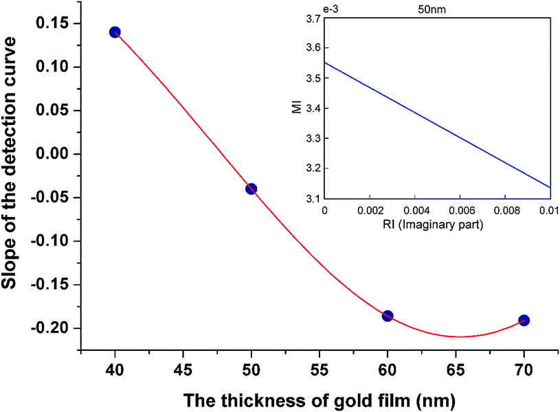 | ||
| Fig. 4 The sensitivity at different thicknesses of the gold film. The inset shows a linear relationship between MI and the imaginary part, obtained from the map. The slopes at different thicknesses so obtained were plotted as the sensitivities. | ||
The slope of the line from the inset in Fig. 4 is extracted whose absolute value is used as the sensitivity. The slopes obtained are plotted against the Au film thickness in Fig. 4 and we see that at a thickness of ∼50 nm, the sensitivity is ∼0.05, whereas for both thinner and thicker Au films, the sensitivity increases in opposite directions. At a thickness of 65 nm, the sensitivity is ∼4 times higher. From this figure and the discussion above, we can infer that for the MI method it is advantageous to deviate as far as possible from the classical wavelength SPR optimum gold thickness, bounded by film thickness able to excite SPR in the Kretschmann configuration. The experimental data in Fig. 3 agree well with these ratios for different thicknesses and point to a conclusion that for a thicker gold film (for example, as required to be able to configure the Au surface for both electrochemistry and SPR), the MI method may be more suitable for the detection of absorbing molecules.
Conclusion
The development of bio- and nano-technology enriches the potential labelling options with complex optical properties. These properties can be associated with the SPR sensing technique by affecting the dielectric constant in both the real and imaginary parts. This results in variations of the SPR wavelength, angle, phase and MI. Many classical dyes also have dielectric properties that will cause changes in both the real and imaginary parts of the dielectric but their potential has not been widely exploited because they generally produce only minor perturbation of the SPR wavelength or angle for optimal 50 nm Au film SPR chips. Nevertheless, such materials have been explored previously using simple evolutionary algorithms to predict useful material properties and non-classical measurement regimes were proposed to achieve the most significant outcomes.12 In this work, we have taken a more holistic approach to considering the dielectric properties of these dyes and the new engineered absorbing materials with their luminescence functions, to consider their capability as labels or amplification layers. Their effect on the MI is mapped in this paper. These maps provide a way for matching label or layer properties for particular SPR conditions and suggest that an Au film thickness that is thicker than that currently used should be considered in these cases. For example, for the thicker gold film (∼65 nm), the MI method is more suitable for the detection of absorbing materials against a non-absorbing background. This suggests stronger potential to be able to visualize both bio-macromolecules and smaller molecular weight compounds with SPR imaging.Acknowledgements
This research is supported by the National Natural Science Foundation of China (NSFC, 31271064), International Exchanges Scheme 2012 China Cost share between Royal Society, UK and NSFC (31311130124), and Fundamental Research Funds for the central University.References
- J. Homola and M. Piliarik, Surface Plasmon Resonance Based Sensors, Springer, Berlin Heidelberg, 2006 Search PubMed.
- J. Homola, S. S. Yee and G. Gauglitz, Sens. Actuators, B, 1999, 54, 3–15 CrossRef CAS.
- M. Piliarik and J. Homola, Opt. Express, 2009, 17, 16505 CrossRef CAS PubMed.
- G. Pelossof, R. Tel-Vered and I. Willner, Anal. Chem., 2012, 84, 3703 CrossRef CAS PubMed.
- J. Chung, S. Kim, R. Bernhardt and J. Pyun, Sens. Actuators, B, 2005, 111, 416 CrossRef.
- S. Kubitschko, J. Spinke, T. Brückner, S. Pohl and S. N. Oranth, Anal. Biochem., 1997, 253, 112 CrossRef CAS PubMed.
- D. Habauzit, S. Bayle, D. Benimelis, J. Chopineau and B. Roig, Arch. Biochem. Biophys., 2014, 541, 61 CrossRef CAS PubMed.
- C. L. Weingart, et al. , Infect. Immun., 1999, 67, 4264 CAS.
- X. Hong and E. A. H. Hall, Analyst, 2012, 137, 4712 RSC.
- G. Leveque and O. J. F. Martin, Opt. Express, 2006, 14, 9971 Search PubMed.
- L. He, M. D. Musick, S. R. Nicewarner, F. G. Salinas, S. J. Benkoric, M. J. Natan and C. D. Keating, J. Am. Chem. Soc., 2000, 122, 9071 CrossRef CAS.
- J. M. Rooney and E. A. H. Hall, Anal. Chem., 2004, 76, 6861 CrossRef CAS PubMed.
- K. Kurihara, K. Nakamura, E. Hirayama and K. Suzuki, Anal. Chem., 2002, 74, 6323 CrossRef CAS PubMed.
- N. Granqvist, A. Hanning, L. Eng, J. Tuppurainen and T. Viitala, Sensors, 2013, 13, 15348 CrossRef CAS PubMed.
- C. Arnold, Y. Zhang and J. G. Rivas, Opt. Express, 2012, 20, 27554 CrossRef PubMed.
- X. Chen, Y. Chen, M. Qiu, R. J. Blaikie and B. Y. Ding, Phys. Status Solidi B, 2015, 252, 2222 CrossRef CAS.
- W. N. Hansen, J. Opt. Soc. Am., 1968, 58, 380 CrossRef.
- D. J. O'Shannessy, M. Brigham-Burke, K. K. Soneson, P. Hensley and I. Brooks, Anal. Biochem., 1993, 212, 457 CrossRef.
Footnote |
| † Electronic supplementary information (ESI) available: Calculation of peak absorption and KD. See DOI: 10.1039/c6ay01890d |
| This journal is © The Royal Society of Chemistry 2016 |