
 Open Access Article
 This Open Access Article is licensed under a Creative Commons Attribution-Non Commercial 3.0 Unported Licence
Chemical energy dissipation at surfaces under UHV and high pressure conditions studied using metal–insulator–metal and similar devices
Detlef
Diesing
and
Eckart
Hasselbrink
Fakultät f. Chemie, Universität Duisburg-Essen, 45141 Essen, Germany. E-mail: Eckart.Hasselbrink@Uni-Duisburg-Essen.de; Fax: +49 201 1833228; Tel: +49 201 1833056
First published on 17th May 2016
Abstract
Metal heterostructures have been used in recent years to gain insights into the relevance of energy dissipation into electronic degrees of freedom in surface chemistry. Non-adiabaticity in the surface chemistry results in the creation of electron–hole pairs, the number and energetic distribution of which need to be studied in detail. Several types of devices, such as metal–insulator–metal, metal–semiconductor and metal–semiconductor oxide–semiconductor, have been used. These devices operate by spatially separating the electrons from the holes, as an internal barrier allows only – or at least favours – transport from the top to the back electrode for one kind of carrier. An introduction into the matter, a survey of the literature and a critical discussion of the state of research is attempted.
 Detlef Diesing | Detlef Diesing obtained his PhD in physics at the Universität Düsseldorf in 1996 in an interdisciplinary work between electrochemistry and surface science. During his postdoctoral stay in Tsukuba (Japan) he became familiar with surface enhanced infrared spectroscopy. He continued this work at the National Institute Forschungszentrum Jülich at the Institut für Grenzflächenforschung and Vakuumphysik. In 2006, he came to the University of Duisburg-Essen to join the collaborative research center “Energy dissipation at surfaces”. |
 Eckart Hasselbrink | Eckart Hasselbrink obtained his PhD in physics at the Universität Göttingen in 1985. After spending two years at Stanford as a postdoc, he became a group leader at the Fritz-Haber-Instut der Max-Planck-Gesellschaft in Berlin in the department of Prof. G. Ertl in 1987. He moved to Odense Universitet, Denmark, in 1987. Since 1998, he has been a full professor at the Universität Essen, later Universität Duisburg-Essen. Prof. Hasselbrink’s research is focussed on surface chemical reaction dynamics, encompassing molecular beam studies, state-resolved studies in surface photochemistry, as well as the dynamics and structuring of organic monolayers. He was awarded the Karl-Scheel Preis by the German Physical Society in Berlin, and the Dozentenstipendium by the Fonds der Chemischen Industrie. He has published more than 100 research papers. Moreover, he served the university as vice-rector for research for five years. |
1 Introduction
Metal–insulator–metal, metal–insulator–semiconductor and metal–semiconductor thin film devices have allowed new light to be shed in recent years on a long standing, fundamental problem in surface chemistry. For more or less pragmatic reasons it has been commonly assumed that the dynamics of reactions at metal surfaces proceeds strictly in the electronic ground state. It is argued that excited electronic states have short lifetimes, and hence exhibit broad widths leading to a large coupling between states such that the system will rapidly collapse to the electronic ground state. However, this argument may also be turned around. As metals have a continuous spectrum of electronic excitations, no chemical process on a metallic surface will proceed without any excitation of electron–hole pairs.1 Hence, it remains a quest to quantify the extent of energy which is transferred into electronic excitations in the course of a surface chemical reaction. Thin film heterostructures have just made such studies possible.Moreover, there is also a strong applied interest in this question. Any excitation of electronic degrees of freedom in the metal substrate can be regarded as a direct conversion of chemical energy into electrical energy. The question arises as to whether these processes are so strong that they promise to be practically applicable for the generation of electricity.2,3 Such a utilisation will require the operation of chemical reactors at large turnover frequencies, implying rather high pressures of the reacting gases and elevated temperatures. Hence, this is the motivation for experiments at conditions closely resembling these.
The decisive aspect of the functionality of thin metal heterostructures in this context is that the structure allows the spatial separation of the excited electrons from the corresponding holes (Fig. 1). Hence, a current can be observed when connecting a meter between the front metal layer and the back side, which is a reflection of the number of electronic excitations created by the surface chemistry per unit time.
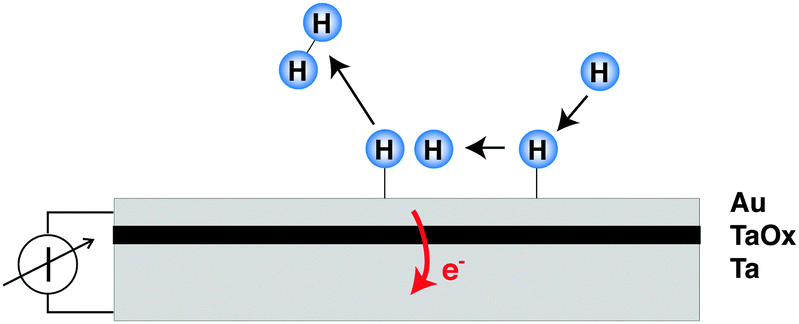 | ||
| Fig. 1 Principle of the application of thin metal film devices for the study of coupling to electronic degrees of freedom in surface chemistry. The chemistry proceeding on the front side goes along with the excitation of electron–hole-pairs, the electrons of which may in this case pass the barrier imposed by the oxide layer, provided they have sufficient energy. The resulting electron flux can externally be detected as a macroscopic current. | ||
The role of non-adiabaticity in surface chemical reactions has recently been reviewed.4–6 A review with special focus on the interplay of hot electrons and metal–oxide interfaces in the context of catalysis has also been prepared recently.7
2 Devices
In recent years, several laboratories have made use of structures which have in common a several nanometer thick metal film that is exposed to a vacuum and its surface supports the chemistry to be studied, while an internal interface serves as a filter for either electron or hole transport. The metal film rests either on a substrate with a thin oxide layer at the interface, or alternatively, the spontaneously formed Schottky space charge layers at metal–semiconductor interfaces have been utilised as such barrier layers. Metal–insulator–metal (MIM) structures have been prepared by us by first electrochemically oxidising a 30 nm thick metal film deposited on glass.8–10 The oxidation process is self-limiting, and determined by the applied potential resulting in a uniform oxide thickness of 3–4 nm.11 On top of this oxide layer, a metal film was deposited with a thickness just large enough to ensure that the film is closed. Thicknesses of 15 nm for Au and 7 nm for Pt have been sufficient to achieve the latter. These films are microcrystalline in structure.The band structure of such a device is illustrated in Fig. 2. If no bias voltage is applied to the device, the Fermi levels of the top metal film and the substrate align. These two systems are separated by the oxide layer which exhibits a band gap. For the barrier materials used by us, Ta, Al and Ti, the width of the band gap ranges between 3 and 5 eV.12,13 The band gap is energetically aligned with the Fermi level of the metal such that the conduction band is closer to the Fermi level than the valence band. Thus, the energy with respect to the band edge required for transport is smaller for electrons than for holes. Moreover, we find a built-in electric field across the oxide, causing the barrier to be skewed like a parallelogram, i.e., the barrier for electrons is larger on the interface towards the top metal film than towards the substrate.
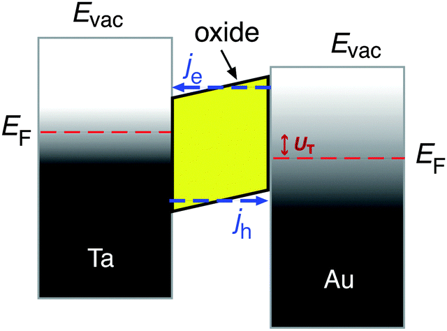 | ||
| Fig. 2 Bandstructure of a Au–Ta metal–insulator–metal thin film device. The oxide layer exhibits a bad gap which insulates the two metal layers for carrier transport at the Fermi level. The barrier due to the band gap in the oxide is skewed due to an electric field across the oxide layer. Moreover, a bias voltage has been applied, resulting in an offset of the Fermi levels of the two metals with respect to each other. The shading indicates the Fermi distribution of electrons at a finite temperature for the Ta layer and that the electronic system in the Au layer has been excited. The arrows indicate the energetically most probable situation for electron and hole transport, respectively. | ||
The carrier transport through such systems was characterised studying the optical response to near-infrared photons.14 The most important finding was that for excitation energies close to the barrier height, electron transport from the top metal to the substrate was always favoured over the reverse transport. This effect was tentatively attributed to energy losses due to electron–phonon scattering in the oxide's conduction band.
Metal–semiconductor (MS) structures have also been used to study the conversion of chemical energy into electronic excitations in the course of surface reactions.2,15,16 In these structures, a Schottky barrier at the buried interface serves as filter for (hot) electrons or alternatively holes (Fig. 3). This depends on the doping of the semiconductor substrate and whether its bands bend up (n-type semiconductor) or bend down (p-type) at the interface due to the formation of a space charge layer. That creates a barrier for electron transport at energies close to the conduction band minimum, or alternatively, for holes, at the top of the valence band. In the first case, this Schottky barrier allows only electrons with excitation energies larger than the barrier height to cross into the conduction band of the semiconductor substrate, whereas the corresponding holes are confined at the interface. In the second case, the roles of electrons and holes are reversed.
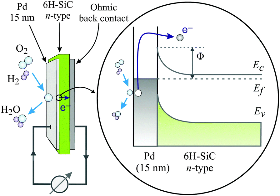 | ||
| Fig. 3 Schematic drawing of the devices used by Karpov and co-workers and their respective band structure. The surface chemistry can induce hot electrons some of which are ballistically transported through the metal film and over the Schottky barrier in the Pd/n-SiC structure. Φ denotes the height of the Schottky barrier, EC denotes the position of the conduction band minimum, EF denotes the Fermi level, and EV denotes the top of the valence band. Reproduced from ref. 15 with permission from AIP, 2015. | ||
A common characteristic of these structures is that a buried oxide layer, or alternatively, the Schottky barrier, serves to separate the chemically excited (hot) electrons from the corresponding holes. As long as the thickness of the top metal film is small enough that the transport to the internal interface is predominantly ballistic – a phrase meaning not encountering inelastic collisions – these devices can be utilised to quantify the electronic excitations arising from the chemistry at the vacuum interface. Schottky barriers typically exhibit heights of 0.5–0.8 eV and the space charge layer extends ≈100 nm into the semiconductor substrate. Hence, tunnelling is exceedingly improbable and the barrier acts as a filter with a sharp threshold energy. However, this statement needs to be softened as in laboratory devices, the Schottky barrier typically exhibits a lateral variation of 0.1–0.2 eV. MIM and metal–insulator–semiconductor (MIS) devices utilise a nanometer-thick oxide layer which serves as a charge carrier filter, but with a threshold energy typically larger than 1 eV. Tunnelling allows carriers with energies somewhat smaller than the barrier to pass the latter. Hence, the filter cuts off less sharply. Moreover, MIM devices allow electrons and holes of sufficient energy to pass the barrier. However, the threshold energies differ for electrons and holes such that transport for one of the two will predominate.
The use of MIM devices to study chemical processes goes back to earlier work by Otto and co-workers in the context of electrochemistry.17 Also, the reverse process – hot electron driven surface chemistry utilising MIM devices – has received considerable interest.18–21 In the applied world they receive interest as sensors.22–24,26 For further reading, we refer to the review by Bănică.25
3 Ultrahigh vacuum studies
Significant progress has been made in the last two decades in unravelling the fundamentals of gas–surface interactions.6,27 Sophisticated experiments and rapid progress in theoretical modelling have contributed to this success.28 Elaborate total energy calculations providing potential energy surfaces and high dimensionality quantum or classical calculations of the dynamics are today state-of-the-art. However, these schemes tacitly assume that the chemical process described evolves adiabatically in the electronic ground state. This is in particular the case whenever density functional theory (DFT) is relied upon. In order to cope with the many nuclear degrees of freedom involved in surface processes, schemes are advantageous which calculate the potential data points ad hoc along with the evolution of a trajectory, for which the term ab initio molecular dynamics (AIMD) has been coined.29,30 There is, however, mounting evidence suggesting that non-adiabatic effects must not be neglected in many important situations.5,31 Experiments, such as the dissociative adsorption of O2 on Al(111)32–35 and the interaction of highly vibrationally excited NO with Cu(111)36 and Cs covered Au(111)37 raise the question whether the non-adiabaticity in surface chemical reactions has not been underestimated in the past. The significance of non-adiabatic effects in dissociative adsorption or recombinative desorption is lively and controversially discussed38,39 based on studies of interaction systems such as H2/Cu(111),40–43 N2/Ru(001)41,44,45 and N2/W(110).42 On the theoretical side, first steps have been undertaken to cope with this challenge.46–51Naturally, there is a quest to have a direct measure of the degree of non-adiabaticity in gas–surface interactions. In seminal work, Nienhaus and co-workers reported the observation of a chemicurrent when a Ag/Si-Schottky diode was exposed to a flux of hydrogen atoms, suggesting that a portion of the chemisorption energy is dissipated to electronic degrees of freedom of the substrate.52 This experiment has stimulated novel theoretical studies.53–58
The experiment of Nienhaus and McFarland showed an initial electron flux of 4.5 × 10⁻⁴ e− per adsorbing H atom (Fig. 4). The signal decreased exponentially with time, which was attributed to the saturation of surface sites with H adatoms. The steady-state current was attributed to the fact that sites became available again due to Eley–Rideal type abstraction reactions.
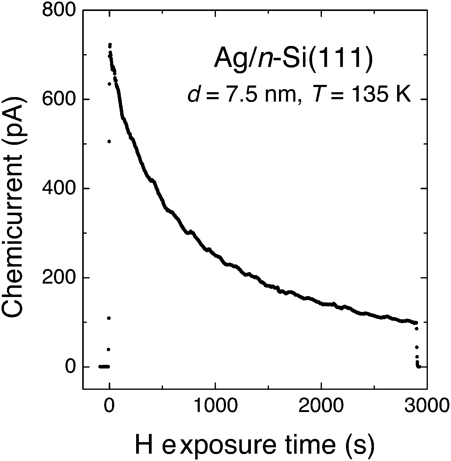 | ||
| Fig. 4 “Chemicurrent” transient observed by Nienhaus and co-workers when exposing a Ag/n-Si(111) Schottky diode to a flux of H atoms. The device was held at 136 K and the thickness of the Ag layer was 7.5 nm. Adapted from ref. 4 with permission from Elsevier, 2015. | ||
Nienhaus and co-workers built on their initial work on hydrogen adsorption52,59 by using Metal/Si Schottky diodes to study the oxidation of alkali60 and Mg films,61 as well as the homoepitaxy of Mg.62
In our laboratory, we have used MIM structures to search for electronic excitations in the course of the interaction of H with and on metal surfaces.8–10 Studies could be carried out over the temperature range from 130 to 350 K due to the negligible sensitivity to visible photons and the smaller thermal noise level of MIMs. Au was the material primarily used for the catalytic surface. The results were compared later on to those obtained with other metals, such as Cu, Ag and Pt.
Analysing the current transients and correlating them with the kinetics of the hydrogen recombination reaction, the following observations could be established: (i) the steady-state current follows the same rate law as the recombination reaction. (ii) If the flux of hydrogen atoms is cycled, the observed transient is in agreement with 2nd order kinetics for the recombination reaction. (iii) A contribution from adsorption or Eley–Rideal type abstraction events can only be of minor importance, although it cannot completely be ruled out. (iv) With the build up of coverage, a displacement current is observed, which is due to the shift of the Fermi level in a nanometer thick metal film when adsorption is accompanied by charge transfer at the surface. (v) The signal scales with the thickness of the top metal layer as is expected from the free path length of electrons at an energy corresponding to the barrier height. Hence, the data suggests that Langmuir–Hinshelwood type recombination events are the predominating source of electronic excitations which are observed as current.
The currents were found to scale as expected when the substrate metal was varied from which the oxide layer was prepared. Al exhibits such a high barrier (2–3 eV depending on the preparation method)12 that no current could be observed. When using Ti instead of Ta, a significantly larger current resulted, as the barrier is smaller (1.2–1.4 eV compared to the 1.7 eV for Ta).63
At this point we may summarise: in Ag/Schottky barrier experiments at TS = 130 K a chemicurrent is observed, which is interpreted to result from H atom adsorption. In experiments using MIM devices at elevated temperatures, a current arising from the LH recombination reaction dominates. These two reports conflict at first glance, but may not necessarily do so. At TS = 130 K, the recombination reaction has a very small rate, such that a current may escape observation in the Nienhaus experiments. Moreover, it may be speculated that a current from the recombination reaction contributes to the steady-state current reported. Experiments at elevated temperature have not been feasible with Schottky diodes due to the thermal noise. In experiments using MIM devices, on the other hand, the electronic excitations arising from adsorption may not have been observable due to the higher barrier in these devices. This reasoning would suggest that H adsorption leads to the excitation of a smaller mean energy than that from the LH recombination reaction. This argument is corroborated by the fact that the current density observed with Schottky devices is about one order of magnitude larger than the one seen with MIM devices. Interestingly, Wodtke and co-workers recently found evidence that the creation of electron–hole pairs mediates strong energy losses in the collision of hyperthermal H atoms with a Au surface.64 Theoretical modelling suggests that the H atoms undergo sequential collisions, transferring on average 0.4 eV each time,65 which would be consistent with the interpretation of the MIM and Schottky device experiments.
Studying different metals as substrates for the chemistry we found: for the coinage metals – Ag and Cu – the findings are qualitatively equal to the ones discussed for Au, but quantitatively different. In contrast, no chemicurrent attributable to the recombination reaction could be observed for Pt.
The interaction of hydrogen with coinage and noble metal surfaces has been subject of innumerable studies.66 The binding energy of H with the various faces of these metals ranges between 260–280 kJ mol−1 for Pt, 230 kJ mol−1 for Cu, and 190–210 kJ mol−1 for Ag and Au.67 Whereas these differences seem only quantitative in nature, the transition state to recombinative desorption has a different character in the case of Pt group metals when compared to the coinage metals.68 In the latter case, the transition state lies energetically 50 to 100 kJ mol−1 above the asymptotic level corresponding to an unbound H2 molecule, with the highest value expected for Au. In the case of Pt, there is no such pronounced maximum in the minimum energy pathway of the molecule away from the surface.69 This is in line with the finding that dissociative H2 adsorption is not activated on Pt group metals, whereas on coinage metal, it is strongly activated.
When using both kinds of devices – MIM sensors or Schottky contacts – marked isotope effects are observed. The signal for H exposure is larger by a factor of about 4 than that for D exposure.8,59 A strong isotope effect is generally seen as a litmus test for non-adiabaticity. The influence of non-adiabatic coupling scales with the velocity of the particle. Hence, comparing two isotopes at the same translational energy, the amount of energy lost due to non-adiabatic effects scales with the square root of the mass ratio. This expectation is reproduced in first principles model calculations using time-dependent DFT.70 As the barrier in the device cuts off low energy excitations, large isotope effects result. Knowing the cut-off energy and assuming a Boltzmann distribution, the parameter characterising this distribution can be derived, which is often expressed as a fictitious temperature. In these studies, values between 2000 and 3000 K are found. If this value is for the moment interpreted as the mean energy of the excitations, then this amounts to some 10 kJ mol−1, i.e. a tenth of a typical chemical binding energy. Interestingly, the reported isotope effect by Nienhaus and co-workers in their experiment is smaller than the one reported by us for experiments using MIMs, which is in line with the suggestion that adsorption results in excitations of lower energy than the recombination reaction.
MIM devices allow one to apply a bias voltage between the two metal layers. As a consequence, the Fermi levels are shifted with respect to each other and the barrier imposed by the band gap in the oxide is distorted (Fig. 1). Depending on polarity, transport from the top layer to the back contact becomes easier for electrons or alternatively holes, while the other type of carriers encounters the opposite effect. Effectively, the median cut-off energies are shifted to lower values on the absolute energy scale, or to higher ones. Alternating the applied allowed bias voltage allows the derivative of the current with respect to the cut-off energy to be obtained, that is, the spectrum in the vicinity of these energy values (Fig. 5). Experiments for H interacting with Au yielded a distribution of electrons with a slope of 1050 K at an energy of 1.4 eV and one for holes with a slope of 1675 K at the cutoff-energy of 2.4 eV. For D atom dosing, smaller values, namely 900 and 1050 K, respectively, were found as expected. These values give a refined picture of the respective distributions when compared to simple estimates derived from the isotope effects.
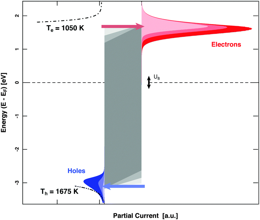 | ||
| Fig. 5 Differential spectroscopy of the energy distribution of the electron and hole flow in a MIM device. By biasing the device, the two Fermi levels are offset with respect to each other. As a consequence electron and hole flow are either eased or hampered. Form the current variation, the slope of the energy distribution in the vicinity of the cut-off energies can be derived; which are 1075 K and 1675 K for the electron and the holes, respectively. | ||
Theoretical work has focused on the non-adiabaticity of atomic hydrogen adsorption. The crossing of the atomic affinity level through the Fermi level of the metal is seen as the critical point along the trajectory, as it gives rise to a spin orthogonalisation catastrophe when discussed within the Newns–Anderson picture.54–57 The latter arises as the H atom carries spin, but the metal is spin unpolarized. Qualitative agreement has been achieved in model calculations. Less theoretical attention has been paid to the recombination process. But recent work has suggested that the motion of hot H atoms on the surface may be connected with large electronic friction.48 Such motion is the precursor to any recombination reaction and, hence, would scale with the rate of this reaction.
4 Higher pressure studies
Studies at pressures large enough to induce currents of macroscopically relevant magnitude in thin film structures have been pioneered by the Somorjai group.71–73 For their initial studies, they used structurally rather complicated Pt/TiO2 and Pt/GaN devices, for which they coined the term catalytic nanodiode. Exposing these devices to a near-stoichiometric flow of CO + O2 at about 104 Pa and elevating the temperature to 400 to 550 °C, they observed steady currents for hours. In a subsequent study of the hydrogen oxidation reaction,74 a yield of 1.1 × 10⁻⁴ electrons per reaction event was derived, by looking at the ratio of the current observed to the turnover frequency (Fig. 6). One question of concern was what the thermoelectric contribution to these currents was. This question was addressed by running experiments in which the devices were exposed to a flow of He. However, it is difficult to account this way for the heating due to the dissipated exothermicity of the chemical reactions.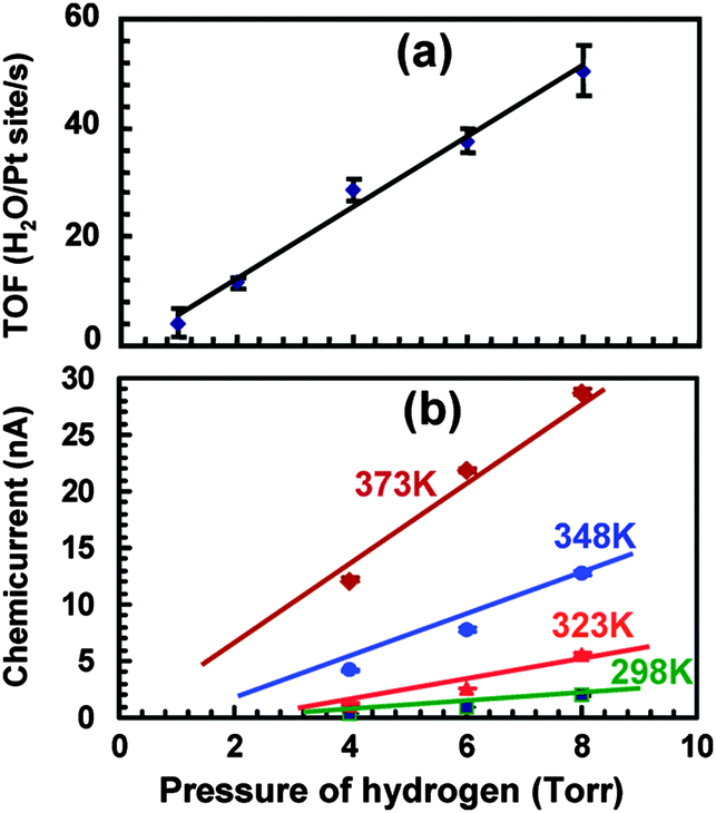 | ||
| Fig. 6 (a) Turnover frequency for different pressures of H2 in 105 Pa of O2 at 353 K. (b) A plot of the chemicurrent as a function of different H2 pressures in 105 Pa of O2. Reprinted with permission from ref. 74. Copyright (2009) American Chemical Society. | ||
Karpov and Nedrygailov studied hydrogen oxidation to water on the surfaces of Pd/n-SiC heterojunction nanostructures (Fig. 3).15 These devices exhibit a Schottky barrier of 0.65 eV, which is similar to Si based devices, but the use of the wide band gap semiconductor SiC allows operation at elevated temperatures necessary to achieve appreciable reaction rates. Currents of up to 7.2 μA at T = 667 K were observed during admission of a stoichiometric oxygen–hydrogen mixture with a pressure of 25 Pa. Upon analysing their data, they concluded that the quantum yield may be as large as 0.2, whereby this property is defined as the number of electrons observed per water formation event. They suggested that the predominant part must be attributed to ballistic electrons as the current would be much larger than what is expected as a thermionic current, based on the Richardson equation.
In a subsequent paper the same authors employed Pd/GaP and Pt/GaP devices with results in line with their earlier conclusions.3 In all these studies, the prime argument was that the current observed scales linearly with the reaction rate.
Creighton and Coltrin16 were able to shed some light on these experiments by building similar devices and modelling the heat flow in such a structure as used by Park and Somorjai. Arguing that the dominant source of a thermoelectric (Seebeck) current is the lateral temperature gradient between the two electric contacts, namely the Ohmic contact to the semiconductor substrate and the electric contact to the metal layer, a simplifying replacement circuit was constructed. Using experimentally determined temperatures for the two spots, a current is predicted which in magnitude and dependence on reaction rate agrees well with what is observed experimentally. The large current in these devices is facilitated by the large Seebeck coefficient of GaN.
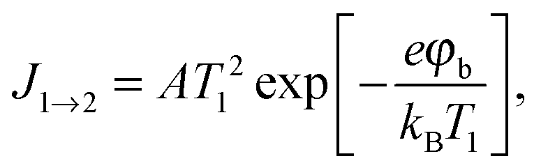
Three possible origins have to be considered for any chemicurrent: (i) the kind of current we discussed for the UHV studies, namely a true chemicurrent arising from electrons, respectively holes, excited in the context of a chemical reaction event and ballistically transported to the internal interface. (ii) A thermionic current arising from a difference in temperatures between the two metal layers which are separated by the barrier. (iii) A thermoelectric current arising from a temperature gradient across any one of the layers due to the finite thermal conductivity. If the two layers separated by the oxide barrier are at different temperatures, an imbalance in their respective (Fermi) distribution of carriers arises. In thermal equilibrium, the electron flow from one layer to the other and vice versa cancels. In the case of a temperature gradient, this is no longer the case, as the hotter layer will contribute a larger number of electrons (“1” in Fig. 7). Hence, a macroscopic current arises, as long as the two layers are shortcircuited. Quantitatively, this current can be accounted for by applying the Bethe equation:
 | (1) |
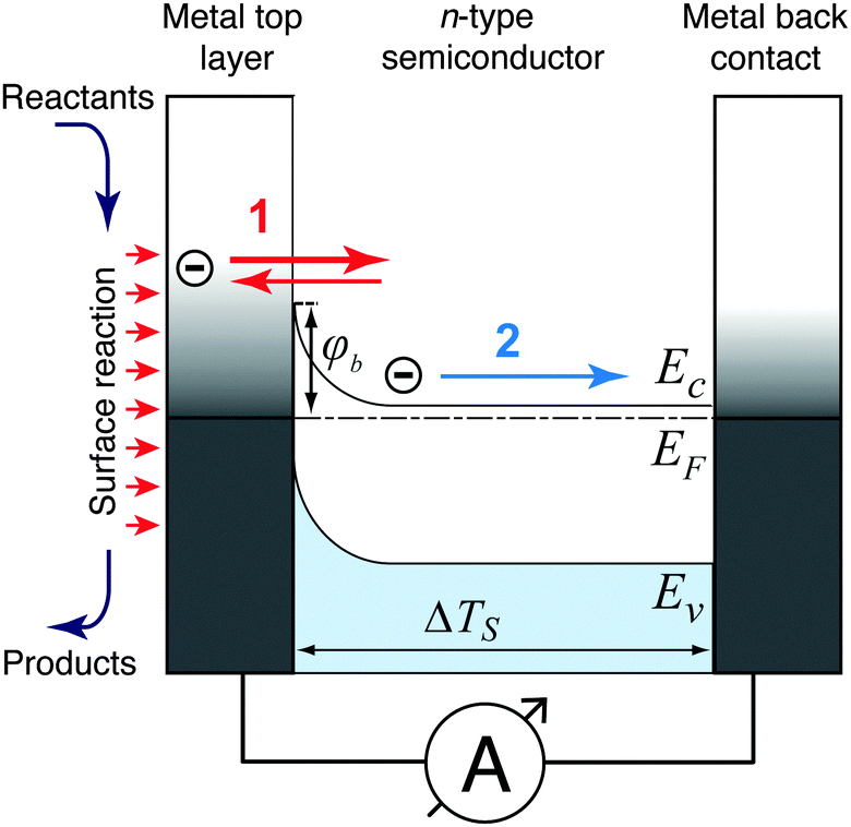 | ||
| Fig. 7 Temperature gradients and resulting charge carrier transport in a metal–semiconductor nanostructure with φb as the Schottky barrier height, EF as the Fermi level, ΔTS as the temperature drop across the semiconductor layer, and EC and EV as the conduction band minimum and top valence band energy, respectively. A thermionic current (1) arises in the case of a temperature drop across the metal–semiconductor interface. The thermoelectric current (2) is due to the Seebeck effect caused by the temperature gradient across the semiconductor layer between the interfaces to the top metal layer and the Ohmic metal back contact. | ||
Thermoelectric currents inside one medium arise due to temperature differences between two boundary surfaces of one medium. The driving force for these currents is the Seebeck voltage, which is induced by a diffusion process of thermally activated charge carriers.75 The dominating charge carriers (electrons in metals and in n-type semiconductors, defect electrons in p-type semiconductors) flow from the hotter edge of the medium to the colder edge, giving rise to a potential difference between the edges of the medium. Non-negligible temperature differences across a medium can be expected when one interface of the medium is heated by the catalysed reactions while the other side is ultimately connected to a heat sink. Such kind of devices were introduced decades ago.76 When the surface of such a device supports a catalyzed reaction with a significant turnover frequency, a heat flow of several 10 mW cm−2 is to be expected.77 The resulting temperature gradient can lead to significant thermoelectric currents, particularly across semiconductor layers. For silicon, the Seebeck coefficient is in the range of 1000 μV K−1,76 and for Ga based systems, one finds values of 300 μV K−1.78 Even in the latter case, the Seebeck coefficient is large enough to expect device currents of the size which have been attributed in some studies to chemicurrents.16
As the top layer is only nanometers thick, no significant temperature drop will exist across it. The same argument holds for the insulating oxide layer in MIM devices. Thus, a thermoelectric current only has to be considered for the back electrode. The comparably low contribution of thermoelectric effects is to be expected for these MIM devices, as the Seebeck coefficient is small for metals.79 For noble metals, the Seebeck coefficient does not exceed 10 μV K−1, and for the catalytically active platinum, the coefficient even becomes zero at 200 K and changes sign.80
In any case, the exothermicity of the chemistry at the vacuum interface is a significant power source causing a temperature gradient across the device, the details of which depend on its design and its suspension in the apparatus. When the back electrode is made from a material with a large Seebeck coefficient, such as most semiconductors, this will be the largest concern. For MIM devices, the thermionic current is likely dominating as the Seebeck coefficients of metals are small.
The problem becomes immediately apparent when one inspects the results depicted in Fig. 8. These have been obtained in a bulb experiment using mixtures of H2 and O2 in the ratio 1![[thin space (1/6-em)]](https://www.rsc.org/images/entities/char_2009.gif) :5 at different pressures.81 The experiment used a Pt/SiOx/Si device. The reaction was started by radiatively heating the Pt film after the gas volume had been filled with the mixture. The top panel shows the evolution of the pressure over time as the reaction proceeds. The rate of the reaction is largest where the descent of the pressure is steepest. This agrees well with the temperature increase, which is read using a tiny Pt1000 sensor attached to the Pt film. The device was hung from thin wires to reduce the heat conduction as far as possible, and thereby minimise temperature gradients in the device. The bottom panel depicts the temporal evolution of the current. One would expect a true chemicurrent to occur in a synchronous manner to the chemical rate. It is immediately obvious that it evolves differently than the temperature measured and to the rate of the chemical reaction. The peak current is observed earlier in time. This experiment clearly suggests that the current cannot solely be attributed to electrons excited in the course of the surface chemical reactions. But it also does not appear to be only a temperature effect.
:5 at different pressures.81 The experiment used a Pt/SiOx/Si device. The reaction was started by radiatively heating the Pt film after the gas volume had been filled with the mixture. The top panel shows the evolution of the pressure over time as the reaction proceeds. The rate of the reaction is largest where the descent of the pressure is steepest. This agrees well with the temperature increase, which is read using a tiny Pt1000 sensor attached to the Pt film. The device was hung from thin wires to reduce the heat conduction as far as possible, and thereby minimise temperature gradients in the device. The bottom panel depicts the temporal evolution of the current. One would expect a true chemicurrent to occur in a synchronous manner to the chemical rate. It is immediately obvious that it evolves differently than the temperature measured and to the rate of the chemical reaction. The peak current is observed earlier in time. This experiment clearly suggests that the current cannot solely be attributed to electrons excited in the course of the surface chemical reactions. But it also does not appear to be only a temperature effect.
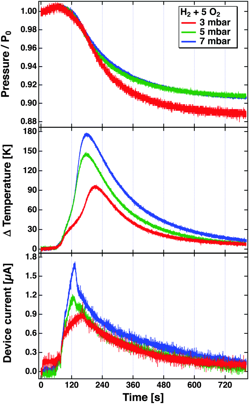 | ||
| Fig. 8 Pressure, temperature increase and device current observed during the reaction of H2 with O2 in a bulb experiment using a Pt/Si device. The bulb (55l) was filled with H2 and O2 in the ratio of 1:5 to total pressures of 3, 5 and 7 mbar. The reaction was initiated at about t = 80 s by irradiating the Pt surface with a light bulb which causes the temperature to rise from room temperature to the ignition temperature.81 | ||
Nedrygailov et al. addressed this problem in model studies.77 Considering a Pt/n-Si device for which the thickness of the Si substrate is 0.525 mm, he calculated the thermionic and thermoelectric current. The chemistry proceeding at the vacuum interface is regarded as a power source. Typical turnover frequencies in bulb experiments correspond to 10−4 to 10−2 W cm−2. For simplicity, it is assumed that the backside is uniformly held at a fixed temperature by the experimental layout, allowing for a one-dimensional model. The first finding is that the thermoelectric current is larger by two orders of magnitude than the thermionic one. The size of the first markedly depends on the temperature at the back of the device (Fig. 9). Between 200 and 600 K, a variation of the current over 12 orders of magnitude is calculated. For conditions typical of bulb experiments, the model predicts a current density of 10−9 to 10−5 A cm−2. This result is remarkable as the temperature difference across the back electrode ranges only between 10−6 to 10−3 K.
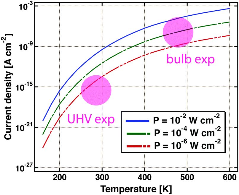 | ||
| Fig. 9 Thermoelectric current density as calculated using a simple model for a Pt/Si device. It is assumed that the Si substrate is 0.5 mm thick. The temperature at the backside of the device is the variable. Three different amounts of power dissipated from a catalysed chemical reaction on the surface are considered, 10−2, 10−4 and 10−6 W cm−2. The coloured circles indicate the regimes in which typical UHV and bulb experiments are operated. Adapted from ref. 77. | ||
Admittedly, the thermoelectric effect is more pronounced in Si-devices than e.g. GaN or TiO2 based ones. But it certainly raises concern that the model suggests currents of a size as typically observed in the bulb experiments. On the other hand, it is reassuring that under UHV experimental conditions, thermoelectric currents between 10−17 to 10−14 A cm−2 are to be expected.
At present, the largest experimental stumbling block is an accurate in situ measurement of the temperature of the catalytic active nano film. With a volume of typically 0.1 mm3, its heat capacity is orders of magnitude smaller than that of the smallest sensor, such as a Pt1000. Optical measurements are hampered by the fact that such thin metal films are optically partially transparent. Indirect ways to measure this temperature have been explored,82,83 but they must not conflict with recording the chemicurrent.
5 Conclusions
Thin film metal heterostructures have allowed new light to be shed on the dissipation of chemical energy into electric excitations on metal surfaces. The findings challenge the unreflected assumption that a surface chemical process will in any case be adiabatic, i.e. follow the ground state potential energy surface. Encouraging strides have been made in theoretical work to account for these experimental findings. Regarding the work under high pressure conditions, it has been found that it is harder than expected to separate direct electronic from subsequent thermal effects. The search for materials with larger conversion efficiencies of chemical to electrical energy is still on.References
- P. W. Anderson, Phys. Rev. Lett., 1967, 18, 1049 CrossRef CAS.
- X. Ji, A. Zuppero, J. M. Gidwani and G. A. Somorjai, Nano Lett., 2005, 5, 753 CrossRef CAS PubMed.
- E. G. Karpov and I. Nedrygailov, Phys. Rev. B: Condens. Matter Mater. Phys., 2010, 81, 205443 CrossRef.
- H. Nienhaus, Surf. Sci. Rep., 2002, 45, 1–78 CrossRef CAS.
- E. Hasselbrink, Curr. Opin. Solid State Mater. Sci., 2007, 10, 192–204 CrossRef.
- K. Golibrzuch, N. Bartels, D. J. Auerbach and A. M. Wodtke, Annu. Rev. Phys. Chem., 2015, 66, 399 CrossRef CAS PubMed.
- J. Y. Park, L. R. Baker and G. A. Somorjai, Chem. Rev., 2015, 115, 2781 CrossRef CAS PubMed.
- B. Mildner, E. Hasselbrink and D. Diesing, Chem. Phys. Lett., 2006, 432, 133 CrossRef CAS.
- B. Schindler, D. Diesing and E. Hasselbrink, J. Phys. Chem. C, 2013, 117, 6337 CAS.
- B. Schindler, D. Diesing and E. Hasselbrink, J. Chem. Phys., 2011, 134, 034705 CrossRef PubMed.
- D. Diesing, A. W. Hassel and M. M. Lohrengel, Thin Solid Films, 1999, 342, 282 CrossRef CAS.
- D. A. Kovács, J. Winter, S. Meyer, A. Wucher and D. Diesing, Phys. Rev. B: Condens. Matter Mater. Phys., 2007, 76, 235408 CrossRef.
- K. Stella, D. A. Kovács, D. Diesing, W. Brezna and J. Smoliner, J. Electrochem. Soc., 2011, 158, P65 CrossRef CAS.
- P. Thissen, B. Schindler, D. Diesing and E. Hasselbrink, New J. Phys., 2010, 12, 113014 CrossRef.
- E. G. Karpov and I. I. Nedrygailov, Appl. Phys. Lett., 2009, 94, 214101 CrossRef.
- J. R. Creighton and M. E. Coltrin, J. Phys. Chem. C, 2012, 116, 1139 CAS.
- D. Diesing, G. Kritzler, M. Stermann, D. Nolting and A. Otto, J. Solid State Electrochem., 2003, 7, 389 CrossRef CAS.
- R. G. Sharpe, S. Dixon-Warren, P. Durston and R. Palmer, Chem. Phys. Lett., 1995, 234, 354 CrossRef CAS.
- J. W. Gadzuk, Phys. Rev. Lett., 1996, 76, 4234 CrossRef CAS PubMed.
- D. Diesing, H. Janssen and A. Otto, Surf. Sci., 1995, 331(3), 289 CrossRef.
- T. Wadayama, A. Kojim and A. Hatta, Appl. Phys. A: Mater. Sci. Process., 2004, 79, 1891 CrossRef CAS.
- K. I. Lundstrom, M. S. Shivaraman and C. M. Svensson, J. Appl. Phys., 1975, 46, 3876–3881 CrossRef CAS.
- L.-G. Ekedahl, M. Eriksson and I. Lundstrom, Acc. Chem. Res., 1998, 31, 249 CrossRef CAS.
- H. Nienhaus, H. S. Bergh, B. Gergen, A. Majumdar, W. H. Weinberg and E. McFarland, J. Vac. Sci. Technol., A, 1999, 17, 1683 CAS.
- F.-G. Bănică, Chemical sensors based on semiconductor electronic devices, John Wiley & Sons, Ltd, 2012, pp. 217–245 Search PubMed.
- D. Sarkar, H. Gossner, W. Hansch and K. Banerjee, Appl. Phys. Lett., 2013, 102, 023110 CrossRef.
- G. R. Darling and S. Holloway, Rep. Prog. Phys., 1995, 58, 1595 CrossRef CAS.
- Handbook of Surface Science, ed. E. Hasselbrink and B. I. Lundqvist, Elsevier, Amsterdam, 2008, vol. 3 Search PubMed.
- M. C. Payne, I. Stich, A. D. Vita, M. J. Gillan and L. J. Clarke, Faraday Discuss. Chem. Soc., 1993, 96, 151 RSC.
- C. Díaz and G. J. Kroes, Chem. Soc. Rev. 10.1039/C5CS00336A.
- A. M. Wodtke, J. C. Tully and D. J. Auerbach, Int. Rev. Phys. Chem., 2004, 23, 513 CrossRef CAS.
- A. J. Komrowski, J. Z. Sexton, A. C. Kummel, M. Binetti, O. Weiße and E. Hasselbrink, Phys. Rev. Lett., 2001, 87, 246103 CrossRef CAS PubMed.
- M. Binetti and E. Hasselbrink, J. Phys. Chem. B, 2004, 108, 14677 CrossRef CAS.
- J. Behler, K. Reuter and M. Scheffler, Phys. Rev. B: Condens. Matter Mater. Phys., 2008, 77, 115421 CrossRef.
- F. Libisch, C. Huang, P. Liao, M. Pavone and E. A. Carter, Phys. Rev. Lett., 2012, 109, 198303 CrossRef PubMed.
- Y. Huang, C. T. Rettner, D. J. Auerbach and A. M. Wodtke, Science, 2000, 290, 111 CrossRef CAS PubMed.
- J. D. White, J. Chen, D. Matsiev, D. J. Auerbach and A. M. Wodtke, Nature, 2005, 433, 503 CrossRef CAS PubMed.
- A. Hodgson, Prog. Surf. Sci., 2000, 63, 1 CrossRef CAS.
- P. Nieto, E. Pijper, G. Laurent, R. A. Olsen, E. J. Baerends, G. J. Kroes and D. Farias, Science, 2006, 312, 86 CrossRef CAS PubMed.
- A. C. Luntz, M. Persson and G. O. Sitz, J. Chem. Phys., 2006, 124, 091101 CrossRef CAS PubMed.
- A. C. Luntz and M. Persson, J. Chem. Phys., 2005, 123, 074704 CrossRef CAS PubMed.
- J. I. Juaristi, M. Alducin, R. D. Muiño, H. F. Busnengo and A. Salin, Phys. Rev. Lett., 2008, 100, 116102 CrossRef CAS PubMed.
- A. S. Muzas, J. I. Juaristi, M. Alducin, R. D. Muiño, G. J. Kroes and C. Daz, J. Chem. Phys., 2012, 137, 064707 CrossRef CAS PubMed.
- L. Diekhöner, L. Hornekær, H. Mortensen, E. Jensen, A. Baurichter, V. V. Petrunin and A. C. Luntz, J. Chem. Phys., 2002, 117, 5018 CrossRef.
- C. Díaz, J. K. Vincent, G. P. Krishnamohan, R. A. Olsen, G. J. Kroes, K. Honkala and J. K. Nørskov, J. Chem. Phys., 2006, 125, 114706 CrossRef PubMed.
- N. Shenvi, S. Roy and J. C. Tully, J. Chem. Phys., 2009, 130, 174107 CrossRef PubMed.
- S. Monturet and P. Saalfrank, Phys. Rev. B: Condens. Matter Mater. Phys., 2010, 82, 075404 CrossRef.
- M. Blanco-Rey, J. I. Juaristi, R. D. Muiño, H. F. Busnengo, G. J. Kroes and M. Alducin, Phys. Rev. Lett., 2014, 112, 103203 CrossRef CAS PubMed.
- K. Golibrzuch, P. R. Shirhatti, I. Rahinov, A. Kandratsenka, D. J. Auerbach, A. M. Wodtke and C. Bartels, J. Chem. Phys., 2014, 140, 044701 CrossRef PubMed.
- M. Grotemeyer and E. Pehlke, Phys. Rev. Lett., 2014, 112, 043201 CrossRef PubMed.
- A. Wodtke, Chem. Soc. Rev. 10.1039/C6CS00078A.
- H. Nienhaus, H. S. Bergh, B. Gergen, A. Majumdar, W. H. Weinberg and E. W. McFarland, Phys. Rev. Lett., 1999, 82, 446–449 CrossRef CAS.
- J. W. Gadzuk, J. Phys. Chem. B, 2002, 106, 8265–8270 CrossRef CAS.
- J. R. Trail, M. C. Graham, D. M. Bird, M. Persson and S. Holloway, Phys. Rev. Lett., 2002, 88, 166802 CrossRef CAS PubMed.
- M. Lindenblatt and E. Pehlke, Phys. Rev. Lett., 2006, 97, 216101 CrossRef CAS PubMed.
- D. M. Bird, M. Mizielinski, M. Lindenblatt and E. Pehlke, Surf. Sci., 2008, 602, 1212–1216 CrossRef CAS.
- M. S. Mizielinski, D. M. Bird, M. Persson and S. Holloway, Surf. Sci., 2008, 602, 2617 CrossRef CAS.
- M. Timmer and P. Kratzer, Phys. Rev. B: Condens. Matter Mater. Phys., 2009, 79, 165407 CrossRef.
- D. Krix, R. Nünthel and H. Nienhaus, Phys. Rev. B: Condens. Matter Mater. Phys., 2007, 75, 073410 CrossRef.
- D. Krix and H. Nienhaus, Appl. Surf. Sci., 2013, 270, 231 CrossRef CAS.
- S. Glass and H. Nienhaus, Phys. Rev. Lett., 2004, 93, 168302 CrossRef CAS PubMed.
- U. Hagemann, M. Timmer, D. Krix, P. Kratzer and H. Nienhaus, Phys. Rev. B: Condens. Matter Mater. Phys., 2010, 82, 155420 CrossRef.
- K. Stella, PhD thesis, Universität Duisburg-Essen, 2011.
- O. Bünermann, H. Jiang, Y. Dorenkamp, A. Kandratsenka, S. M. Janke, D. J. Auerbach and A. M. Wodtke, Science, 2015, 350, 1346–1349 CrossRef PubMed.
- S. M. Janke, D. J. Auerbach, A. M. Wodtke and A. Kandratsenka, J. Chem. Phys., 2015, 143, 124708 CrossRef PubMed.
- K. Christmann, Adsorbate properties of hydrogen on solid surfaces, Springer, Berlin, 2006, vol. III/42A.5, p. 111 Search PubMed.
- P. Ferrin, S. Kandoi, A. U. Nilekar and M. Mavrikakis, Surf. Sci., 2012, 606, 679–689 CrossRef CAS.
- B. Hammer and J. K. Nørskov, Surf. Sci., 1995, 343, 211 CrossRef CAS.
- E. Pijper, G. J. Kroes, R. A. Olsen and E. J. Baerends, J. Chem. Phys., 2002, 117, 5885 CrossRef CAS.
- M. Lindenblatt and E. Pehlke, Surf. Sci., 2006, 600, 5068–5073 CrossRef CAS.
- X. Z. Ji and G. A. Somorjai, J. Phys. Chem. B, 2005, 109, 22530–22535 CrossRef CAS PubMed.
- X. Ji, A. Zuppero, J. M. Gidwani and G. A. Somorjai, J. Am. Chem. Soc., 2005, 127, 5792–5793 CrossRef CAS PubMed.
- J. Y. Park and G. A. Somorjai, ChemPhysChem, 2006, 7, 1409–1413 CrossRef CAS PubMed.
- A. Hervier, J. R. Renzas, J. Y. Park and G. A. Somorjai, Nano Lett., 2009, 9, 3930–3933 CrossRef CAS PubMed.
- T. H. Geballe and G. W. Hull, Phys. Rev., 1955, 98, 940–947 CrossRef CAS.
- W. Fulkerson, J. P. Moore, R. K. Williams, R. S. Graves and D. L. McElroy, Phys. Rev., 1968, 167, 765–782 CrossRef CAS.
- I. I. Nedrygailov, E. G. Karpov, E. Hasselbrink and D. Diesing, J. Vac. Sci. Technol., A, 2013, 31, 021101 Search PubMed.
- E. N. Hurwitz, M. Asghar, A. Melton, B. Kucukgok, L. Su, M. Orocz, M. Jamil, N. Lu and I. T. Ferguson, J. Electron. Mater., 2010, 40, 513–517 CrossRef.
- B. Schindler, D. Diesing and E. Hasselbrink, Z. Phys. Chem., 2013, 227, 1381 CAS.
- N. Cusack and P. Kendall, Proc. Phys. Soc., 1958, 72, 898 CrossRef.
- I. I. Nedrygailov, D. Diesing and E. Hasselbrink, unpublished.
- I. I. Nedrygailov, E. Hasselbrink, D. Diesing, S. K. Dasari, M. A. Hashemian and E. G. Karpov, J. Vac. Sci. Technol., A, 2012, 30, 030601 Search PubMed.
- J. P. Meyburg, I. I. Nedrygailov, E. Hasselbrink and D. Diesing, Rev. Sci. Instrum., 2014, 85, 104102 CrossRef PubMed.
| This journal is © The Royal Society of Chemistry 2016 |