
 Open Access Article
 This Open Access Article is licensed under a Creative Commons Attribution-Non Commercial 3.0 Unported Licence
Charge carrier loss mechanisms in CuInS2/ZnO nanocrystal solar cells†
Dorothea
Scheunemann
*,
Sebastian
Wilken
,
Jürgen
Parisi
and
Holger
Borchert
Energy and Semiconductor Research Laboratory, Department of Physics, University of Oldenburg, Carl-von-Ossietzky-Straße 9–11, 26129 Oldenburg, Germany. E-mail: dorothea.scheunemann@uni-oldenburg.de
First published on 20th May 2016
Abstract
Heterojunction solar cells based on colloidal nanocrystals (NCs) have shown remarkable improvements in performance in the last decade, but this progress is limited to merely two materials, PbS and PbSe. However, solar cells based on other material systems such as copper-based compounds show lower power conversion efficiencies and much less effort has been made to develop a better understanding of factors limiting their performance. Here, we study charge carrier loss mechanisms in solution-processed CuInS2/ZnO NC solar cells by combining steady-state measurements with transient photocurrent and photovoltage measurements. We demonstrate the presence of an extraction barrier at the CuInS2/ZnO interface, which can be reduced upon illumination with UV light. However, trap-assisted recombination in the CuInS2 layer is shown to be the dominant decay process in these devices.
1 Introduction
Colloidal nanocrystal (NC) solar cells have made remarkable progress within the last decade, with power conversion efficiencies approaching 10%.1–5 This development was encouraged by a deeper understanding of the underlying physical processes in NC solids and devices, in particular, regarding the role of charge transport,6–8 defect states,9–11 doping,12–14 surface passivation,15 and interface recombination.16,17 However, the vast majority of these studies is focused on merely two materials, PbS and PbSe.18,19 In contrast, there is still a lack of such detailed knowledge in the case of other NC materials, such as copper-based compounds. For several reasons, including ecological aspects, these materials are considered to be a relevant alternative to lead chalcogenides for photovoltaic applications.20,21 However, without extensive post-processing, the device performance remains comparatively low to date.22–27Recently, we studied NC solar cells based on a CuInS2/ZnO heterojunction.28,29 We could show that charges are only collected from a narrow region within the CuInS2 layer (collection zone), located in the proximity of the heterojunction.29 This limitation may be a consequence of a low mobility-lifetime (μτ) product,30 as well as insufficient doping of the metal oxide.31 Both effects would impede charge transport within the absorber. Moreover, even within the collection zone, the collection probability was found to be restricted to only ∼50%,29 indicating a serious loss of excess carriers in the devices. Basically, two possible mechanisms might play a role here: first, charge recombination in the volume of the absorber layer (bulk recombination), which is known to occur in NC layers via three possible processes of different reaction orders δ: (i) Shockley–Read–Hall (SRH) recombination via deep trap states (δ = 1),7,32 (ii) direct band–band decay (δ = 2),33,34 and (iii) Auger recombination (δ = 3);6,35 second, energetic barriers for the extraction/injection of charges at one of the electrodes or recombination at the absorber/metal oxide interface (interface recombination).
Regarding the latter, however, studies on the metal oxide film in NC solar cells are rare and mostly focused on the introduction of external dopants16,36,37 or surface passivation,38 both of which have an impact on the interfacial recombination processes. In our previous work on CuInS2/ZnO solar cells,28,29 we observed that light soaking under UV containing light leads to a significant improvement of the device characteristics. Similar effects have been observed in organic solar cells employing an interfacial layer of ZnO NCs.39–41 In this context, it was shown that UV illumination results in an increase of the carrier density in the ZnO due to the release of chemisorbed oxygen species, a process which is often referred to as photodoping.41–44
In this article, we present a detailed study on the photocurrent loss mechanisms in CuInS2/ZnO heterojunction solar cells. Therefore, steady-state characterization methods using different illumination conditions were employed to clarify the effect of UV light in our devices. Moreover, we used transient photocurrent (TPC) and transient photovoltage (TPV) studies, in order to elucidate the dynamics of the present recombination mechanisms. Using this approach, it will be shown that two different loss mechanisms can be distinguished: an extraction barrier at the CuInS2/ZnO interface, which can be reduced upon illumination with UV light, as well as significant bulk recombination in the CuInS2 layer, which is identified as trap-assisted SRH recombination.
2 Results
2.1 Photovoltaic performance as a function of light intensity
We fabricated CuInS2/ZnO heterojunction solar cells with indium tin oxide (ITO)/poly(3,4-ethylenedioxythiophene):poly(styrenesulfonate) (PEDOT:PSS)/CuInS2 NCs/ZnO NCs/Al, according to previous reports.28,29 As demonstrated in Fig. S1 (ESI†), the current density–voltage (J–V) curves of the as-prepared devices exhibit a pronounced S-shape behavior, resulting in a low short-circuit current density (Jsc) and a fill factor (FF), whereas the S-shape is gradually reduced upon illumination with simulated sunlight (light soaking). Previously, such a behavior was assigned to photodoping of the ZnO layer, caused by the UV part of the solar spectrum.28,29 To test this hypothesis and clarify the role of UV light, we used two independent light sources in the following: a white-light (WL) LED with a spectral bandwidth of ∼400–700 nm and a UV LED with a dominant wavelength of λ = 365 nm. In the former case, the ZnO is transparent, ensuring that photogeneration is solely taking place in the CuInS2 layer, whereas, in the latter case, photodoping of the ZnO is facilitated.Fig. 1a shows the intensity-dependent J–V response under WL illumination (no UV content). These illumination conditions result in a deformation of the J–V curves in the fourth quadrant, in particular, a pronounced S-shape with an inflection point located below the voltage axis intercept (J < 0), which becomes even more prominent with increasing WL intensity. Consequently, we observed a reduction of the FF in the absence of UV light. In contrast, Fig. 1b shows that the S-shape disappears once an UV component is added to the WL illumination. Additionally, Jsc exhibits a 2-fold increase compared to the case of only WL illumination, which cannot be explained solely by additional photogeneration due to illumination with UV light (as can be seen from the upper curve in Fig. 1b, only 0.18 mA cm−2 are generated by the UV component).
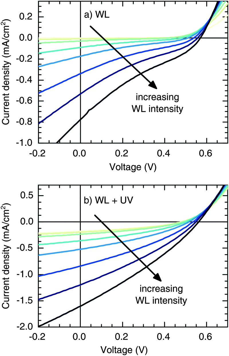 | ||
| Fig. 1 Intensity dependent J–V characteristics of CuInS2/ZnO solar cells under different spectral illumination conditions. (a) White-light (WL) illumination with a spectral bandwidth of ∼400–700 nm at intensities of 0, 0.01, 0.02, 0.08, 0.15, 0.29, 0.47, and 0.70 Suns. (b) The same illumination conditions with an additional UV component (λ = 365 nm). | ||
The light intensity dependence of Jsc is shown in Fig. 2a. It can be seen that the scaling of Jsc with the WL intensity (I), and thus the dominant recombination mechanism at short circuit, is independent of the presence of UV light. The experimental data were fitted to Jsc ∝ Iα, resulting in a linear scaling (α ≅ 1) in both cases, which indicates that recombination losses occur mainly through a first-order process, such as SRH recombination. Additionally, significant losses in Jsc due to space charge effects can be excluded, as α = 0.75 would be expected in that case.45 Apart from that, Fig. 2b shows a slight decrease of the FF with increasing illumination intensity in the presence of UV light. However, compared to the benefit of the UV light itself, this effect is of minor importance. The strong drop in the FF upon switching off the UV light marks the transition from normal to S-shaped J–V behavior.
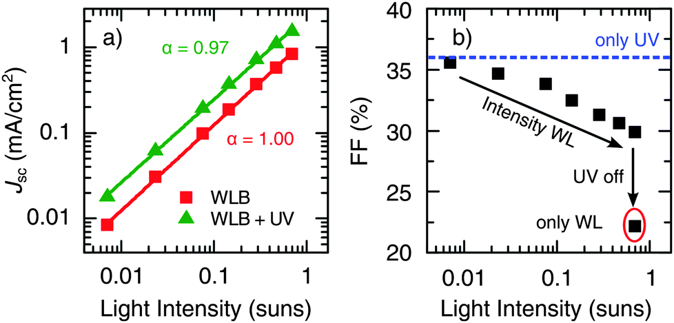 | ||
| Fig. 2 Dependence of the (a) short-circuit current density Jsc and (b) fill factor FF on the incident WL illumination intensity (I). The experimental data (symbols) in (a) are fitted to Jsc ∝ Iα (solid lines). Measurements were performed without (squares) and with (triangles) additional UV illumination. Note that in the latter case Jsc was corrected for the additional photocurrent generated by the UV LED. | ||
In addition, we studied the conductivity of the ZnO thin film depending on the illumination conditions and the surrounding ambient gas (see Fig. S2 and Table S1, ESI†). Under an inert atmosphere, the conductivity increased from 1.4 × 10⁻³ S m−1 in the dark to 3.3 × 10⁻¹ S m−1 upon illumination with UV light. The same trend was observed under ambient conditions; however, absolute values were found to be three to four orders of magnitude smaller (5.6 × 10⁻⁶ S m−1 and 4.4 × 10⁻⁵ S m−1 without and with UV illumination, respectively). These results are in line with a previous publication,41 where the increased photoconductivity as compared to the dark conductivity is associated with the desorption of chemisorbed oxygen species, as will be discussed in more detail below (see Section 3).
2.2 Effect of light-soaking on the spectral dependence of the photocurrent
In order to investigate the effect of UV light soaking on the spectral dependence of the photocurrent, we measured the external quantum efficiency (EQE) under continuous UV background illumination. Therefore, the same UV light source as for the J–V measurements was used. Fig. 3 shows the evolution of the EQE spectrum (symbols) as a function of the UV exposure time. With increasing exposure, the EQE is strongly increased at all wavelengths, which coincides with the trends observed in the J–V measurements (see inset). Moreover, there is also a slight effect on the spectral shape of the EQE, as can be seen more clearly from normalized EQE data (see Fig. S3, ESI†). Similar effects have been reported on PbS/ZnO NC solar cells by Willis et al.31 The authors assigned the improved EQE to a transition of the devices from excitonic to p–n behavior, related to variations of the space-charge region width due to photodoping of the ZnO layer.31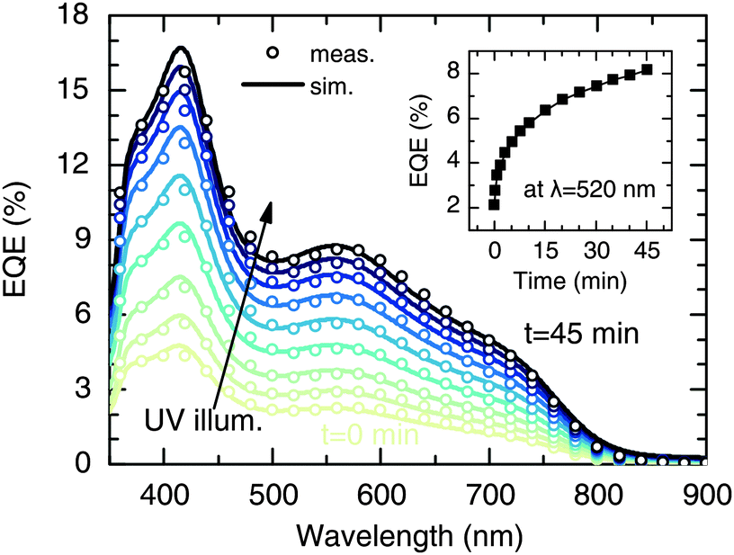 | ||
| Fig. 3 Comparison of the measured (symbols) and reconstructed (straight lines) EQE spectra for a representative device as a function of exposure time to an additional UV bias illumination (λ = 365 nm). The inset shows the evolution of the EQE signal at 520 nm depending on the time the sample was illuminated with UV light. | ||
Here, we use a reconstruction approach to quantify the effect of the UV bias on charge collection, as described previously.29 In general, the EQE is given by
 | (1) |
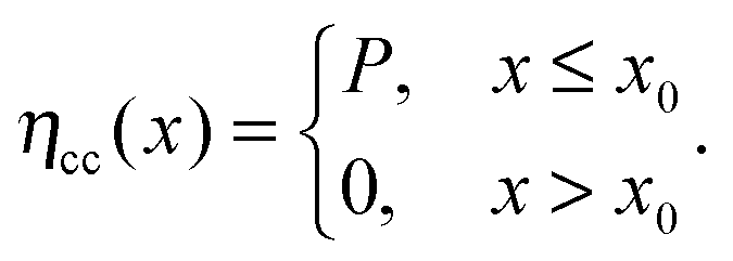 | (2) |
Fig. 4 shows the variation of the parameters x0 and P as a function of UV exposure time. It is clearly seen that the improvement of the EQE is mainly related to an increase of P (Fig. 4a), which increased significantly from 0.3 to 0.7 after 45 min of UV illumination. In contrast, the UV light had only a slight effect on the width of the collection zone (Fig. 4b), which, in terms of the total layer thickness, increased from x0/d = 0.19 to 0.26. This finding is consistent with the fact that there is only little change of the spectral shape of the EQE (see Fig. 3). Hence, in contrast to the work of Willis et al.,31 a significant growth of the depletion region upon photodoping appears unlikely from our data. Instead, it can be suggested that the presence of UV light leads to a higher transfer rate of photogenerated carriers across the CuInS2/ZnO interface. This may be a consequence of a reduced extraction barrier, as will be discussed in Section 3. We note that similar trends regarding the charge collection are observed when the EQE is measured under a reverse bias voltage.29
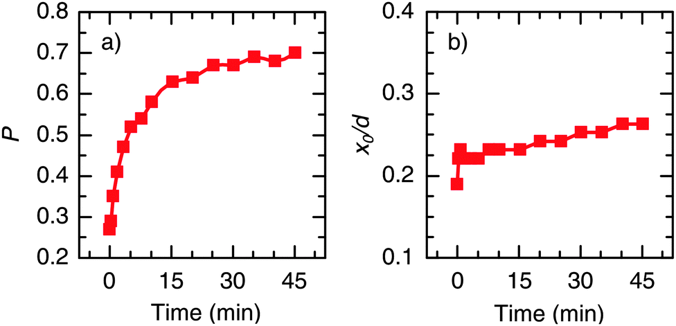 | ||
| Fig. 4 Evolution of the extracted parameters (a) P and (b) x0 (normalized to the absorber thickness d) from the reconstruction of the EQE spectra with UV bias illumination time (see eqn (2) for definition of the parameters). | ||
2.3 Illumination and voltage dependent TPC studies
Next, we studied the dynamics of charge collection using TPC measurements. Fig. 5 shows the photocurrent decay after 500 μs square-pulse excitation (λ = 520 nm) with respect to the following background illumination conditions: (i) no background illumination (dark), (ii) only UV illumination, (iii) only WL illumination (∼0.7 Suns), and (iv) simultaneous UV and WL illumination (WL + UV). From these data, two main processes can be distinguished (see arrows in Fig. 5). First, the presence of UV light results in an increase of the initial signal height by a factor of 2, which is consistent with the 2-fold increase of Jsc described in Section 2.1. However, the decay dynamics itself remains relatively unchanged. Both under dark and UV-only conditions, a long photocurrent tail is observed with charges being collected over hundreds of μs. Such behavior is commonly assigned to the release of carriers from trap states.46 Second, the presence of WL illumination leads to a significant acceleration of the decay and the disappearance of the long-lived tail. This effect is independent of the presence of UV light and, therefore, most likely a consequence of trap-filling within the CuInS2 layer. | ||
| Fig. 5 Transient photocurrent decay at zero voltage bias with respect to different background illumination conditions: no background illumination (black line), only UV light (blue line), only WL (red line), WL + UV (green line). | ||
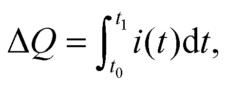
To study the latter effect in more detail, we conducted TPC measurements under WL-only background illumination conditions as a function of the WL intensity. From the raw data depicted in Fig. S4 (ESI†), it can be seen that both the rise and decay dynamics of the photocurrent become significantly faster with increasing intensity. For a quantitative analysis, we calculated the total amount of extracted charge,
 | (3) |
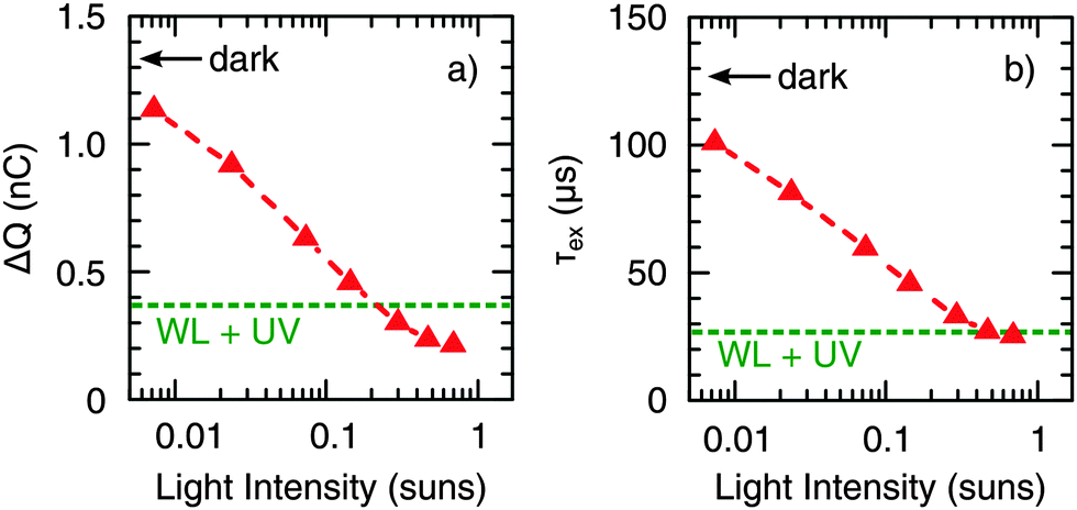 | ||
| Fig. 6 (a) Total amount of extracted charge ΔQ and (b) effective extraction lifetime τex obtained from TPC measurements as a function of the intensity of the continuous WL background illumination. Arrows and dashed lines indicate the values obtained under dark conditions and the presence of an additional UV component (at a fixed WL intensity of 0.7 Suns), respectively. | ||
Furthermore, we conducted voltage dependent TPC measurements by applying an external bias voltage to the devices. Fig. 7 shows a strong decrease of ΔQ (Fig. 7a) and τex (Fig. 7b) with increasing forward bias under dark conditions (the applied voltage was corrected for the voltage drop over the sum of the series and load resistance). This is the same trend as observed for increasing WL background illumination intensity (cf.Fig. 6); hence, it is suggested that trap-filling can also be mediated by carrier injection. Accordingly, the voltage dependence of ΔQ and τex nearly disappeared under the presence of WL illumination, again being independent of the presence of an additional UV component. As discussed earlier,29 CuInS2 is probably not fully depleted under short circuit conditions, so that a significant portion of the absorber can be considered as the quasi-neutral region, where the transport is limited by diffusion. Therefore, we expect the voltage-independent diffusion component of the extraction time to be much larger than the drift component in the range of voltage investigated. This leads to an extraction time independent of voltage under WL illumination, as seen in Fig. 7b. A voltage-independent extraction time for small applied voltage bias was also observed by other authors in the case of partially depleted layers.47,48
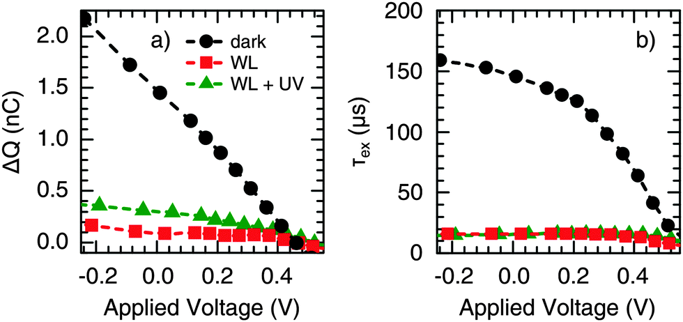 | ||
| Fig. 7 Dependence of (a) ΔQ and (b) τex on the applied bias voltage under different background illumination conditions: no background illumination (black circles), solely WL illumination (red squares), and WL + UV illumination (green triangles). | ||
In addition, under WL-only conditions, so-called overshoots were observed when the applied voltage reaches the inflection point noticed in steady-state J–V measurements (V ∼ 0.45 V, see Fig. S5, ESI†). Previously, such a behavior has been attributed to an energetic barrier for charge extraction.49 In the presence of UV illumination, however, the overshoots were significantly reduced, in accordance with an effective reduction of the extraction barrier, as suggested in Section 2.1.
2.4 Ideality factor and TPV measurements
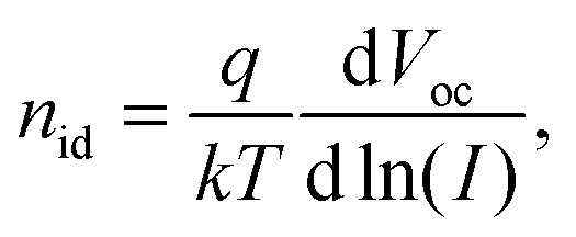
While TPC studies provide information on the dynamics of charge collection, investigations on the photovoltage decay using TPV measurements can be used to study charge recombination. For this purpose, the device is held at open circuit under continuous WL illumination, while the photovoltage decay induced by a light pulse is recorded. The measured voltage signal can be described by V(t) = Voc + ΔV(t), where Voc is the constant open-circuit voltage due to WL illumination and ΔV(t) the transient decay. Light intensities are chosen such that the pulse can be considered as small perturbation, ΔV(t) ≪ Voc.In general, the relationship between Voc and the light intensity I is given by the ideality factor nid,50
 | (4) |
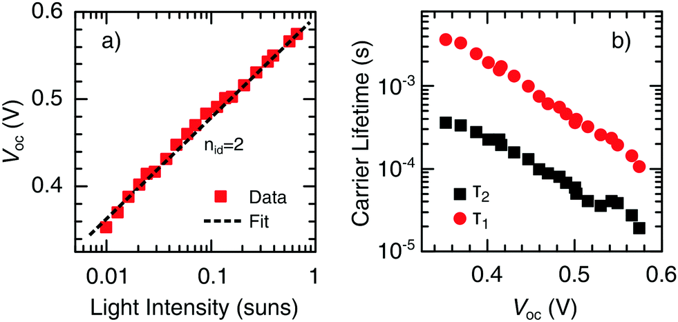 | ||
| Fig. 8 (a) Incident light intensity dependence of Voc. The dashed line represents a fit of the experimental data (symbols) to eqn (4), resulting in an ideality factor of nid = 2. (b) Decay time constants τ1 and τ2 as a function of Voc obtained from TPV measurements. Different steady-state values of Voc were obtained by varying the background WL intensity. | ||
The transient decay ΔV(t) is commonly described by a sum of one or more exponentials. As demonstrated in Fig. S6 (ESI†), a reasonable fit to our data can be obtained by using a biexponential decay function, according to
ΔV(t) = A1![[thin space (1/6-em)]](https://www.rsc.org/images/entities/char_2009.gif) exp(−t/τ1) + A2exp(−t/τ2), exp(−t/τ1) + A2exp(−t/τ2), | (5) |
3 Discussion and conclusions
To summarize our work up to this point, two different loss mechanisms could be identified, related to (i) charge extraction at the CuInS2/ZnO interface and (ii) recombination in the bulk of the CuInS2 layer. Regarding the first point, we showed that the extraction of charge carriers could be significantly improved by selective excitation of the ZnO layer with UV light, resulting in a 2-fold increase of Jsc and the EQE (see Sections 2.1 and 2.2). In principle, this enhancement may be a consequence of an increase of the space-charge region width, as photodoping will significantly increase the charge carrier density in the ZnO. Such an effect with respect to UV exposure has been demonstrated in the case of PbS/ZnO NC solar cells by Willis et al.31 By reconstructing experimental EQE data (see Section 2.2), we showed that UV illumination increases the collection probability within a certain collection zone in the absorber, but, however, does not lead to a significant enlargement of the zone itself, in contrast to ref. 31.Moreover, exposure to UV light had clear impact on the shape of the J–V curves, in particular, the pronounced S-shape present under only WL illumination disappeared, once an UV component is added. Recently, Sandberg et al.53 presented an extensive numerical study to clarify the effect of imperfect contacts leading to S-shaped J–V characteristics. In detail, they used numerical drift-diffusion modeling to study the case of organic solar cells, but their outcomes should be generally applicable to other systems, such as NC solar cells. According to that analysis, the occurrence of the S-shape, as well as the position of the inflection point at J < 0, can be rationalized by a reduced carrier mobility near the electrode interface.53 This is consistent with the reduced conductivity of the ZnO layer in the absence of UV light (see Fig. S2, ESI†), which we previously attributed to electron depletion at the ZnO surface caused by chemisorption of oxygen,41
| O2(g) + e− → O2−(ad), | (6) |
| h+ + O2−(ad) → O2(g), | (7) |
The second, probably more important loss mechanism, is bulk recombination in the CuInS2 layer. Steady-state J–V measurements revealed a linear scaling of the photocurrent with light intensity (see Section 2.1), indicating that the dominant recombination process occurs via a first order process, such as trap-assisted SRH recombination, independent of the presence of UV light. In addition, TPC measurements show a quickening of the decay dynamics with increasing WL intensity, accompanied by the disappearance of the long-lived photocurrent tail (see Section 2.3). Such a light intensity dependence may be related to an increase of the effective carrier mobility due to trap-filling caused by background illumination.8,57 We observed similar effects with increasing external bias voltage, suggesting that trap-filling can also be induced by injected charge carriers.
The significance of trap-assisted recombination, limiting the carrier diffusion and the drift length and, thus, carrier collection and device efficiency, is supported by an ideality factor of nid = 2, as determined from the light intensity dependence of Voc (see Section 2.4). Moreover, two decay channels were observed in TPV measurements, which were not affected by the presence of UV light. Hence, it is assumed that the two decay channels can be assigned to different trap populations in the bulk of the CuInS2 layer, rather than to a combination of bulk and interface recombination. This assumption is in line with the results of other authors.10,58
Trapping phenomena are a well known issue in NC solar cells.9,15,16,59 In particular, Nagpal et al.8 proposed that the mechanism of charge transport in NC films changes under illumination compared to dark conditions: under illumination, charge transport is dominated by a conductive network of quantized band-edge states, while charge transport in the dark is proposed to occur via a weakly conductive mid-gap band. Other authors discussed this increase in conductivity as well, but assigned the role of states with low conductivity to the strongly localized ground states of NCs, while photoexcited states show a much higher mobility.6 Recently, Bozyigit et al.7 demonstrated that the dark current is mediated by trap-assisted recombination, whereas the recombination mechanism is controlled by the diffusion of mobile carriers towards trapped carriers of opposite polarity. However, such detailed studies are to date limited to binary semiconductors such as PbS and PbSe. In principle, a more complicated defect chemistry can be expected in the case of a ternary compound such as CuInS2. In this context, it has been shown that the ratio of Cu/In plays a crucial role in defining the defect levels in the band gap in the case of CuInS2,60,61 while the amount of surface defect states can be influenced by the choice of appropriate ligands or using core shell NCs.62,63
In summary, we were able to identify two different loss mechanisms in our devices, namely a barrier to charge extraction at the CuInS2/ZnO interface and trap-assisted recombination in the bulk of the CuInS2 layer. While the barrier for charge extraction can be reduced by illuminating the device with UV light, recombination of charge carriers via trap states is probably the main reason for the limited charge collection probability and efficiency. This underlines the importance of investigations on trap states in NC solar cells, which is strongly entangled with the question of an appropriate ligand-exchange strategy. However, in the case of CuInS2, this is still under investigation. In consequence, reducing the amount of sub-band gap states is substantial to improve the performance of CuInS2/ZnO solar cells.
4 Experimental details
4.1 Sample preparation
Wurtzite-type CuInS2 NCs (edge length 12 to 18 nm) were synthesized using a hot-injection technique and subjected to a ligand exchange with 1-hexanethiol, as described previously.28,64 Spherical ZnO NCs with an average diameter of 5 nm were synthesized according to ref. 41. Solar cells were fabricated with the device structure of glass/ITO/PEDOT:PSS (40 nm)/CuInS2 NCs (90 nm)/ZnO NCs (60 nm)/Al (120 nm), where the numbers in parenthesis denote the film thickness, as determined by a stylus profiler (Veeco Dektak). The NC films were spin-cast in a nitrogen-filled glove box from chlorobenzene and chloroform/methanol solution, respectively. After deposition of both CuInS2 and the ZnO layer, the samples were annealed at 180 °C. Finally, the Al electrode was thermally evaporated under high vacuum (10−6 mbar). The active area (∼14 mm2) was delimited by the geometric overlap of the ITO and the metal electrode.4.2 Steady-state characterization
J–V characteristics under AM1.5G illumination were recorded using a semiconductor characterization system (Keithley 4200) under ambient conditions. The samples were illuminated using a class AAA simulator (Photo Emission Tech.), providing a simulated AM1.5G spectrum. The light intensity was adjusted to 100 mW cm−2 using a calibrated silicon solar cell. Light intensity dependent measurements were performed using a 4 W white LED (Seoul P4; λ ∼ 400–700 nm), connected to a DC constant-current supply, and variable neutral density filters. A UV LED (Nitride NS365L-5RLO, λ = 365 nm) served as an additional light source (and kept at a constant intensity). EQE measurements were performed using a custom-built setup (Bentham PVE300), equipped with a dual xenon/quartz halogen lamp and a Czerny–Turner monochromator (Bentham TMc300). The monochromatic probe light was modulated by a mechanical chopper at a frequency of 230 Hz. The photocurrent was recorded under short-circuit conditions using a lock-in amplifier (Stanford Research SR 830). The same UV LED mentioned above was used to provide an additional light bias. The reconstruction of the EQE spectra, based on one-dimensional transfer-matrix method simulations, was carried out as described in ref. 29.4.3 Transient techniques
TPC and TPV measurements were carried out using a 4 W green LED (Seoul P4, λ = 525 nm, 250 ns rise/fall time), driven by a two-channel pulse generator (Agilent 81150A). Continuous WL and UV background illumination was provided from the same LED light sources as described above. Transient signals were recorded using a 1 GHz digital storage oscilloscope (Tektronix DPO7104), with an input impedance of 50 Ω (TPC) or 1 MΩ (TPV). The second output channel of the pulse generator (operating in DC mode) was used to apply an external bias for voltage-dependent TPC measurements. A biased Si photodetector (Thorlabs DET36A) was included to the setup to monitor the switching dynamics of the pulse LED, as well as the relative intensity of the background illumination. The intensity in fractions of suns was estimated by comparing the photocurrent generated from the WL LED with that obtained under simulated AM1.5G illumination.Acknowledgements
The authors thank Manuela Schiek for valuable discussions and proofreading. Financial support from the EWE-Nachwuchsgruppe “Dünnschichtphotovoltaik” by the EWE AG, Oldenburg, Germany, is gratefully acknowledged.References
- I. Gur, N. A. Fromer, M. L. Geier and A. P. Alivisatos, Science, 2005, 310, 462–465 CrossRef CAS PubMed.
- A. G. Pattantyus-Abraham, I. J. Kramer, A. R. Barkhouse, X. Wang, G. Konstantatos, R. Debnath, L. Levina, I. Raabe, M. K. Nazeeruddin, M. Grätzel and E. H. Sargent, ACS Nano, 2010, 4, 3374–3380 CrossRef CAS PubMed.
- C.-H. M. Chuang, P. R. Brown, V. Bulović and M. G. Bawendi, Nat. Mater., 2014, 13, 796–801 CrossRef CAS PubMed.
- A. J. Labelle, S. M. Thon, S. Masala, M. M. Adachi, H. Dong, M. Farahani, A. H. Ip, A. Fratalocchi and E. H. Sargent, Nano Lett., 2015, 15, 1101–1108 CrossRef CAS PubMed.
- G.-H. Kim, F. P. G. de Arquer, Y. J. Yoon, X. Lan, M. Liu, O. Voznyy, Z. Yang, F. Fan, A. H. Ip, P. Kanjanaboos, S. Hoogland, J. Y. Kim and E. H. Sargent, Nano Lett., 2015, 15, 7691–7696 CrossRef CAS PubMed.
- A. Shabaev, A. L. Efros and A. L. Efros, Nano Lett., 2013, 13, 5454–5461 CrossRef CAS PubMed.
- D. Bozyigit, W. M. M. Lin, N. Yazdani, O. Yarema and V. Wood, Nat. Commun., 2015, 6, 6180 CrossRef CAS PubMed.
- P. Nagpal and V. I. Klimov, Nat. Commun., 2011, 2, 486 CrossRef PubMed.
- D. Bozyigit, S. Volk, O. Yarema and V. Wood, Nano Lett., 2013, 13, 5284–5288 CrossRef CAS PubMed.
- C.-H. M. Chuang, A. Maurano, R. E. Brandt, G. W. Hwang, J. Jean, T. Buonassisi, V. Bulović and M. G. Bawendi, Nano Lett., 2015, 15, 3286–3294 CrossRef CAS PubMed.
- P. Stadler, B. R. Sutherland, Y. Ren, Z. Ning, A. Simchi, S. M. Thon, S. Hoogland and E. H. Sargent, ACS Nano, 2013, 7, 5757–5762 CrossRef CAS PubMed.
- P. R. Brown, D. Kim, R. R. Lunt, N. Zhao, M. G. Bawendi, J. C. Grossman and V. Bulović, ACS Nano, 2014, 8, 5863–5872 CrossRef CAS PubMed.
- O. Voznyy, D. Zhitomirsky, P. Stadler, Z. Ning, S. Hoogland and E. H. Sargent, ACS Nano, 2012, 6, 8448–8455 CrossRef CAS PubMed.
- S. J. Oh, N. E. Berry, J.-H. Choi, E. A. Gaulding, T. Paik, S.-H. Hong, C. B. Murray and C. R. Kagan, ACS Nano, 2013, 7, 2413–2421 CrossRef CAS PubMed.
- A. H. Ip, S. M. Thon, S. Hoogland, O. Voznyy, D. Zhitomirsky, R. Debnath, L. Levina, L. R. Rollny, G. H. Carey, A. Fischer, K. W. Kemp, I. J. Kramer, Z. Ning, A. J. Labelle, K. W. Chou, A. Amassian and E. H. Sargent, Nat. Nanotechnol., 2012, 7, 577–582 CrossRef CAS PubMed.
- B. Ehrler, K. P. Musselman, M. L. Böhm, F. S. F. Morgenstern, Y. Vaynzof, B. J. Walker, J. L. MacManus-Driscoll and N. C. Greenham, ACS Nano, 2013, 7, 4210–4220 CrossRef CAS PubMed.
- N. Zhao, T. P. Osedach, L.-Y. Chang, S. M. Geyer, D. Wanger, M. T. Binda, A. C. Arango, M. G. Bawendi and V. Bulović, ACS Nano, 2014, 4, 3743–3752 CrossRef PubMed.
- I. J. Kramer and E. H. Sargent, Chem. Rev., 2014, 114, 863–882 CrossRef CAS PubMed.
- G. H. Carey, A. L. Abdelhady, Z. Ning, S. M. Thon, O. M. Bakr and E. H. Sargent, Chem. Rev., 2015, 115, 12732–12763 CrossRef CAS PubMed.
- J. Kolny-Olesiak and H. Weller, ACS Appl. Mater. Interfaces, 2013, 5, 12221–12237 CAS.
- C.-W. Chen, D.-Y. Wu, Y.-C. Chan, C. C. Lin, P.-H. Chung, M. Hsiao and R.-S. Liu, J. Phys. Chem. C, 2015, 119, 2852–2860 CAS.
- Y. Wu, C. Wadia, W. Ma, B. Sadtler and A. P. Alivisatos, Nano Lett., 2008, 8, 2551–2555 CrossRef CAS PubMed.
- Q. Guo, H. W. Hillhouse and R. Agrawal, J. Am. Chem. Soc., 2009, 131, 11672–11673 CrossRef CAS PubMed.
- V. A. Akhavan, B. W. Goodfellow, M. G. Panthani, D. K. Reid, D. J. Hellebusch, T. Adachi and B. A. Korgel, Energy Environ. Sci., 2010, 3, 1600–1606 CAS.
- C. J. Stolle, M. G. Panthani, T. B. Harvey, V. A. Akhavan and B. A. Korgel, ACS Appl. Mater. Interfaces, 2012, 4, 2757–2761 CAS.
- D. Aldakov, A. Lefrançoisa and P. Reiss, J. Mater. Chem. C, 2013, 1, 3756–3776 RSC.
- J. E. Halpert, F. S. F. Morgenstern, B. Ehrler, Y. Vaynzof, D. Credgington and N. C. Greenham, ACS Nano, 2015, 9, 5857–5867 CrossRef CAS PubMed.
- D. Scheunemann, S. Wilken, J. Parisi and H. Borchert, Appl. Phys. Lett., 2013, 103, 133902 CrossRef.
- D. Scheunemann, S. Wilken, J. Parisi and H. Borchert, ACS Photonics, 2015, 2, 864–875 CrossRef CAS.
- T. Kirchartz, J. Bisquert, I. Mora-Seró and G. Garcia-Belmonte, Phys. Chem. Chem. Phys., 2015, 17, 4007–4014 RSC.
- S. M. Willis, C. Cheng, H. E. Assender and A. A. R. Watt, Nano Lett., 2012, 12, 1522–1526 CrossRef CAS PubMed.
- I. J. Kramer, D. Zhitomirsky, J. D. Bass, P. M. Rice, T. Topuria, L. Krupp, S. M. Thon, A. H. Ip, R. Debnath, H.-C. Kim and E. H. Sargent, Adv. Mater., 2012, 24, 2315–2319 CrossRef CAS PubMed.
- V. I. Klimov, J. Phys. Chem. B, 2006, 110, 16827–16845 CrossRef CAS PubMed.
- B. Omogo, J. F. Aldana and C. D. Heyes, J. Phys. Chem. C, 2013, 117, 2317–2327 CAS.
- V. I. Klimov, A. A. Mikhailovsky, D. W. McBranch, C. A. Leatherdale and M. G. Bawendi, Science, 2000, 287, 1011–1013 CrossRef CAS PubMed.
- H. Liu, J. Tang, I. J. Kramer, R. Debnath, G. I. Koleilat, X. Wang, A. Fisher, R. Li, L. Brzozowski, L. Levina and E. H. Sargent, Adv. Mater., 2011, 23, 3832–3837 CrossRef CAS PubMed.
- R. Hoye, B. Ehrler, M. Böhm, D. Muñoz-Rojas, R. Altamimi, A. Alyamani, Y. Vaynzof, A. Sadhanala, G. Ercolano, N. Greenham, R. Friend, J. MacManus-Driscoll and K. Musselman, Adv. Energy Mater., 2014, 4, 1301544 Search PubMed.
- J. Chang, Y. Kuga, I. Mora-Seró, T. Toyoda, Y. Ogomi, S. Hayase, J. Bisquert and Q. Shen, Nanoscale, 2015, 7, 5446–5456 RSC.
- C. E. Small, S. Chen, J. Subbiah, C. M. Amb, S.-W. Tsang, T.-H. Lai, J. R. Reynolds and F. So, Nat. Photonics, 2012, 6, 115–120 CrossRef CAS.
- S. R. Cowan, P. Schulz, A. J. Giordano, A. Garcia, B. A. MacLeod, S. R. Marder, A. Kahn, D. S. Ginley, E. L. Ratcliff and D. C. Olson, Adv. Funct. Mater., 2014, 24, 4671–4680 CrossRef CAS.
- S. Wilken, J. Parisi and H. Borchert, J. Phys. Chem. C, 2014, 118, 19672–19682 CAS.
- R. Gurwitz, R. Cohen and I. Shalisha, J. Appl. Phys., 2014, 115, 033701 CrossRef.
- A. J. Morfa, B. I. MacDonald, J. Subbiah and J. J. Jasieniak, Sol. Energy Mater. Sol. Cells, 2014, 124, 211–216 CrossRef CAS.
- M. Ghosh, R. S. Ningthoujam, R. K. Vatsa, D. Das, V. Nataraju, S. C. Gadkari, S. K. Gupta and D. Bahadur, J. Appl. Phys., 2011, 110, 054309 CrossRef.
- V. D. Mihailetchi, J. Wildeman and P. W. M. Blom, Phys. Rev. Lett., 2005, 94, 126602 CrossRef CAS PubMed.
- C. R. McNeill, I. Hwang and N. C. Greenham, J. Appl. Phys., 2009, 106, 024507 CrossRef.
- J. Hofhuis, J. Schoonman and A. Goossens, J. Appl. Phys., 2008, 103, 014503 CrossRef.
- K. W. Johnston, A. G. Pattantyus-Abraham, J. P. Clifford, S. H. Myrskog, S. Hoogland, H. Shukla, E. J. D. Klem, L. Levina and E. H. Sargent, Appl. Phys. Lett., 2008, 92, 122111 CrossRef.
- W. Tress, S. Corvers, K. Leo and M. Riede, Adv. Energy Mater., 2013, 3, 873–880 CrossRef CAS.
- T. Kirchartz, F. Deledalle, P. S. Tuladhar, J. R. Durrant and J. Nelson, J. Phys. Chem. Lett., 2013, 4, 2371–2376 CrossRef CAS.
- W. Shockley and J. W. T. Read, Phys. Rev., 1952, 87, 835–842 CrossRef CAS.
- Z. Li, F. Gao, N. C. Greenham and C. R. McNeill, Adv. Funct. Mater., 2011, 21, 1419–1431 CrossRef CAS.
- O. J. Sandberg, M. Nyman and R. Österbacka, Phys. Rev. Appl., 2014, 1, 024003 CrossRef.
- A. O. Pudov, A. Kanevce, H. A. Al-Thani, J. R. Sites and F. S. Hasoon, J. Appl. Phys., 2005, 97, 064901 CrossRef.
- C.-H. Chung, B. Bob, T.-B. Song and Y. Yang, Sol. Energy Mater. Sol. Cells, 2014, 120(part B), 642–646 CrossRef CAS.
- V. A. Akhavan, M. G. Panthani, B. W. Goodfellow, D. K. Reid and B. A. Korgel, Opt. Express, 2010, 18, A411–A420 CrossRef CAS PubMed.
- C. G. Shuttle, R. Hamilton, J. Nelson, B. C. O'Regan and J. R. Durrant, Adv. Funct. Mater., 2010, 20, 698–702 CrossRef CAS.
- A. K. Rath, F. Pelayo Garcia de Arquer, A. Stavrinadis, T. Lasanta, M. Bernechea, S. L. Diedenhofen and G. Konstantatos, Adv. Mater., 2014, 26, 4741–4747 CrossRef CAS PubMed.
- K. S. Jeong, J. Tang, H. Liu, J. Kim, A. W. Schaefer, K. Kemp, L. Levina, X. Wang, S. Hoogland, R. Debnath, L. Brzozowski, E. H. Sargent and J. B. Asbury, ACS Nano, 2012, 6, 89–99 CrossRef CAS PubMed.
- D. H. Jara, S. J. Yoon, K. G. Stamplecoskie and P. V. Kamat, Chem. Mater., 2014, 26, 7221–7228 CrossRef CAS.
- P.-H. Chuang, C. C. Lin and R.-S. Liu, ACS Appl. Mater. Interfaces, 2014, 6, 15379–15387 CAS.
- Y.-K. Kim, S.-H. Ahn, K. Chung, Y.-S. Cho and C.-J. Choi, J. Mater. Chem., 2012, 22, 1516–1520 RSC.
- L. Li, A. Pandey, D. J. Werder, B. P. Khanal, J. M. Pietryga and V. I. Klimov, J. Am. Chem. Soc., 2011, 133, 1176–1179 CrossRef CAS PubMed.
- M. Kruszynska, H. Borchert, J. Parisi and J. Kolny-Olesiak, J. Am. Chem. Soc., 2010, 132, 15976–15986 CrossRef CAS PubMed.
Footnote |
| † Electronic supplementary information (ESI) available. See DOI: 10.1039/c6cp01015f |
| This journal is © the Owner Societies 2016 |