
 Open Access Article
 This Open Access Article is licensed under a Creative Commons Attribution-Non Commercial 3.0 Unported Licence
All-2D material photonic devices
Sejeong
Kim
 *
*
Department of Electrical and Electronic Engineering, University of Melbourne, Australia. E-mail: Sejeong.kim@unimelb.edu.au
First published on 4th January 2023
Abstract
Two-dimensional (2D) materials are extensively used in almost all scientific research areas, from fundamental research to applications. Initially, 2D materials were integrated with conventional non-2D materials having well-established manufacturing methods. Recently, the concept of constructing photonic devices exclusively from 2D materials has emerged. Various devices developed to date have been demonstrated based on monolithic or hetero 2D materials. In this review, photonic devices that solely consist of 2D materials are introduced, including photonic waveguides, lenses, and optical cavities. Exploring photonic devices that are made entirely of 2D materials could open interesting prospects as they enable the thinnest devices possible because of their extraordinarily high refractive index. In addition, unique characteristics of 2D materials, such as high optical anisotropy and spin orbit coupling, might provide intriguing applications.
 Sejeong Kim | Sejeong Kim is a lecturer at the University of Melbourne, Australia. She obtained her PhD in Physics from Korea Advanced Institute of Science and Technology (KAIST) in 2014. She was a research fellow at the University of Technology Sydney (UTS). Her research focuses on exploring light–matter interaction at the nanoscale, particularly using optical/plasmonic cavities. This includes studies of photonic crystal cavities for microlasers, sensors and quantum applications, as well as developing an integrated photonics platform. |
1 Introduction
Two-dimensional (2D) materials have become important in almost all fields of research, including electronics, photonics, and material engineering. To this point, numerous favorable characteristics of 2D materials have been reported. For instance, graphene has exceptionally high thermal and electrical conductivities, and its electrical conductivity is comparable to or slightly higher than that of silver.1 Transition metal dichalcogenides (TMDs) have a direct energy bandgap in their monolayer form, which enables the use of 2D materials as a light emitting material. Such thin light emitting materials are traditionally manufactured by growing a thin semiconductor layer, i.e., a quantum well, with a smaller energy bandgap. 2D light emitting materials can be combined with any other materials, whereas quantum well growth is constrained by lattice match between the substrate and the quantum well. Moreover, 2D materials are now promising candidates for quantum light sources and optoelectronic devices.2In the early stages of 2D material-based devices, particularly for photonics applications, 2D materials were integrated with devices made of conventional bulk materials with well-established fabrication technology, such as Si, SiN, SiO2etc. It was only recently that scientists have begun to develop optical devices using exclusively 2D materials. This raised interesting research questions such as can a monolayer guide light?3 Can layered materials serve as optical cavities?4 Exploring all-2D material photonic devices will generates fruitful discussions.
Here, we provide an overview of recent developments in the use of stand-alone 2D materials for optical components. Multiple photonic devices are presented using solely 2D materials and various functioning optical devices are demonstrated. This includes the vast majority of essential optical components, such as waveguides, cavities, and modulators. All-2D material devices were combined with emerging research areas: metaphotonics and Mie-tronics, which are covered in this review. Studying monolithic 2D photonic devices necessitates precise optical parameters, such as refractive index and absorption, which were recently determined by experimental measurements of exfoliated 2D materials. Perspectives and opportunities on stand-alone 2D materials devices are discussed.
2 Discussions
2.1 Light guiding in 2D materials
A waveguide is an essential component of all integrated photonic circuits. In order to guide light, photonic waveguides typically have a thickness of λ/2neff. As the dimension of the waveguide decreases, light is weakly guided and susceptible to bending loss. To create thin waveguides, a high refractive index is required; however, the refractive index of common semiconductors is restricted between 2 to 4 at visible wavelength, and often declines as wavelength increases. To obtain a high refractive index, a material having excitonic resonance at visible wavelengths can be used. In this regard, TMDs are promising material not only because they have excitonic resonance at visible wavelength but also their excitonic resonance is strong. This is because of the reduced dielectric screening and enhanced coulomb interaction. Fig. 1a shows the binding energy and optical bandgap of different 2D materials in their bulk and monolayer forms.5 The high binding energy indicates higher stability and a high refractive index, which allow for ultrathin photonic devices.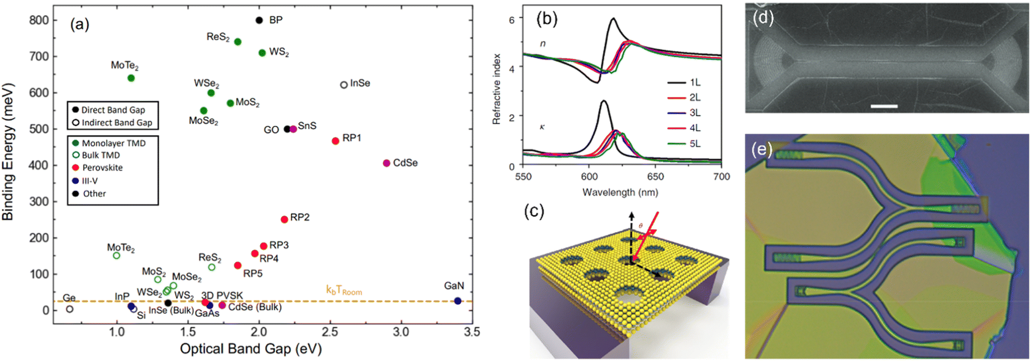 | ||
| Fig. 1 Photonic waveguides. (a) Binding energy versus optical band gap of common 2D semiconductors.5 Copyright 2022 AIP Publishing. (b) Thickness dependent refractive indices of WS2.3 (c) A schematic of the WS2 photonic crystal membrane.3 Copyright 2019 Springer Nature Limited. (d) An hBN waveguide with input and output couplers.6 (e) Optical image of waveguide splitter patterned on a single hBN flake.7 Copyright 2021 American Chemical Society. | ||
Light guiding in a sub nanometer-thick TMD layer was initially predicted in theory.8 In 2019, visible light guiding using angstrom-thick WS2 was experimentally achieved.3Fig. 1b depicts the layer-dependent refractive index and absorption of WS2. An abnormally high refractive index can be achieved with single or few layers WS2. The challenge of the aforementioned experiment was to distinguish the guided mode from the propagating light in free space. They utilised a periodic suspended structure (Fig. 2c) to allow a portion of the guided mode to decay out of the plane of the material. This is possible because a patterned photonic crystal structure folds the waveguide mode dispersion, which normally lies below the light line, back to the first Brillouin zone.
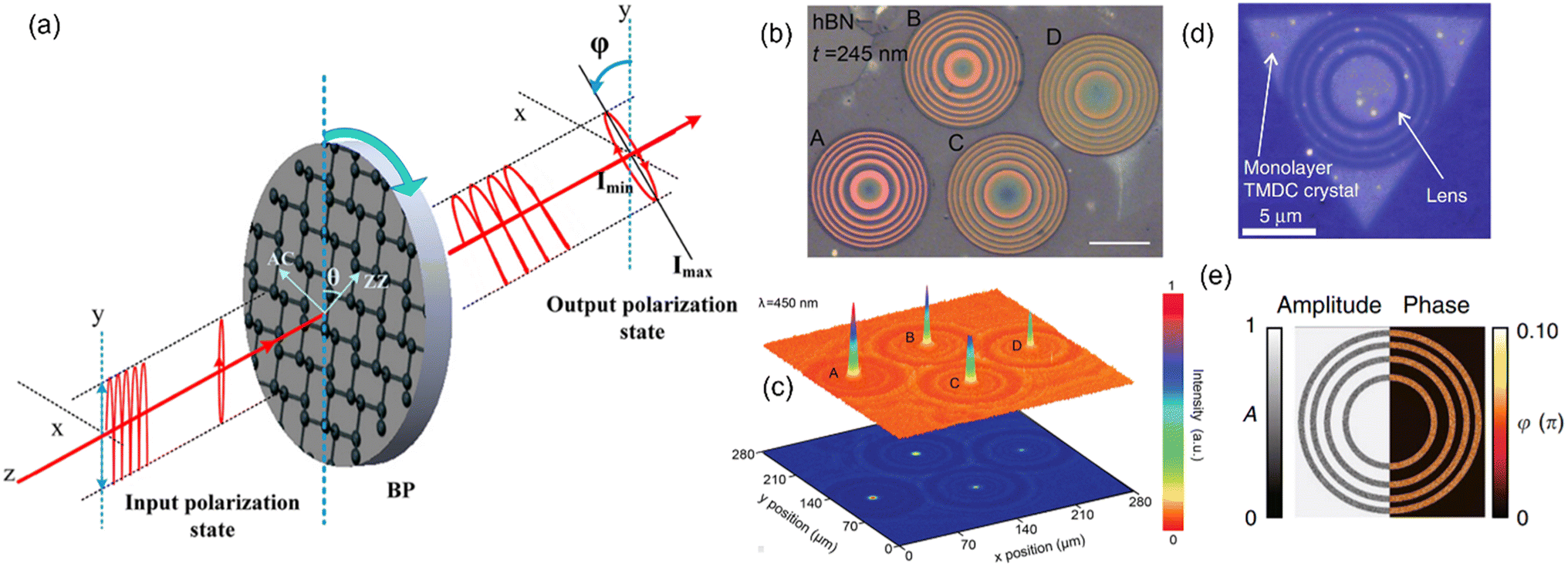 | ||
| Fig. 2 Thin and flat optics. (a) Schematic diagram showing the linearly polarized incident light changes to elliptical polarization state.10 Reprinted with permission from ACS Photonics. Copyright 2017 American Chemical Society. (b) Optical image of the hBN metalenses.11 (c) Intensity distribution at the focal plane. Copyright 2018 American Chemical Society. (d) Optical microscopic image of a monolayer WSe2 lens.12 (e) Simulated amplitude and phase distributions of the WSe2 lens.12 | ||
Wire-type waveguides6 and slot waveguides7 also have been demonstrated. These studies used a 2D insulating material, hexagonal boron nitride (hBN), to construct on-chip waveguides. In contrast to TMDs, hBN has a wide bandgap, and hence the material is transparent for visible wavelengths. And on chip waveguide fully consists of 2D materials (Fig. 1d) is first demonstrated in 2019. In 2021, hBN waveguides were successfully integrated with single photon emitters.7 Some defects in the hBN crystalline structure function as single photon emitters, which naturally allows hBN waveguides to accommodate quantum emitters monolithically. This study also includes a waveguide splitter and inversely designed couplers (Fig. 1e).
Waveguides composed of 2D materials are interesting because they can carry optical signals generated from 2D materials such as photoluminescence (PL), quantum emission, valley polarization, etc. According to a recent theoretical study, material with gyroelectric permittivity can carry intrinsic optical spin and be directed in the medium.9 A gyroelectric medium is a material with non-zero off-diagonal components in the dielectric tensor and shows an anisotropic response to circularly polarized light. In their numerical calculation, model parameters adopted standard values for 2D materials, and it was demonstrated that the waveguide utilizing gyroelectric material can act as an optical spin sorter. Such handedness-selective coupling of light in a waveguide can be potentially integrated into quantum emitters and valley polarized emission.
2.2 Thin and flat optics using 2D materials
Substituting 2D materials for bulky optical systems allow for the miniaturisation of these systems. Several optical components, including waveplates and lenses, have been presented thus far. In order to create waveplates, the photonic device should impose phase retardation to a specific polarization. There are multiple materials that exhibit birefringence at visible wavelength, including black phosphorous (BP), ReS2 and ReSe2, whose birefringence corresponds to 0.245, 0.037, and 0.047, respectively.10 When linearly polarized light propagates through BP, ReS2, and ReSe2, polarization plane rotates by 0.05°, 0.02°, and 0.011° degrees per atomic layer according to ref. 10. Therefore, by varying the thickness of birefringent 2D materials, it is possible to change the level of phase retardance, creating half or quarter waveplates.Ultrathin lenses have also been demonstrated using other 2D materials. In Fig. 2b, hBN metalenses consisting of an array of pillars are shown and their intensity distribution at the focal plane is presented in Fig. 2c.11 In this study, focusing light was possible with limited phase coverage, i.e., a system that does not provide a full 2π phase shift. In the same study, metalenses with an array of MoS2 pillars were fabricated to perform efficient lens focusing at longer wavelength.12 MoS2 was chosen for its high refractive index. It is highlighted that metalenses with 2D materials alleviate fabrication constraints. For example, it is difficult to directly grow common bulk high index materials, such as AlGsAs (n ∼ 3.8) or GaP (n ∼ 3.4) on any substrates, whereas hBN or MoS2 can be exfoliated and transferred. In this work, the thickness of the lens was decreased down to ∼λ/10.
The ultimate thickness for a flat lens is a monolayer. However, it is challenging to obtain sufficient phase modulation with a single layer despite the extraordinarily large refractive indices of TMDs in the visible wavelength range. In order to achieve desired amplitude and phase modulation using sub-nanometer lenses, direct femtosecond laser writing was employed to pattern lenses in monolayer TMDs.12 A femtosecond laser creates size-controlled nanoparticles; for example, WOx is formed from WSe2. An optical microscope image of a patterned monolayer WSe2 lens is shown in Fig. 2d. The refractive index of the monolayer WSe2 is 5.5 at a wavelength of 633 nm while the patterned area has WO2 nanoparticles with a refractive index 1.8 at λ = 633 nm. This allows 0.1 π-phase modulation based on an analytical model (Fig. 2e). In this paper, focusing has been experimentally demonstrated using various 2D materials: WSe2, MoS2, WS2, PtSe2, and PtS2.
2.3 2D material optical cavities
Optical cavities can enhance the light–matter interaction. They increase the spontaneous emission rate, reduce the lifetime, and hence increase the brightness. Early studies on 2D materials utilized the transfer method, i.e., the placement of 2D materials atop optical or plasmonic cavities to take advantage of the cavity effect. Optical cavities were only recently constructed from 2D materials. In 2018, monolithic free-standing photonic crystal cavities were demonstrated using hBN.4 In this study, the layered material was evaluated for nanofabrication using both electron beam lithography and FIB. The highest experimental Q-factor was 2100. In 2022, hBN photonic crystal cavities with an improved Q-factor of 5000 (Fig. 3a) were reported.13Fig. 3a shows an optical microscope image of hBN photonic cavities patterned on a hBN flake. A SEM image of a hBN photonic crystal cavity is shown in Fig. 3b. Here, hBN photonic crystal cavities incorporate single photon emitters. This study demonstrated cavity resonance tuning via temperature (Fig. 3c) and observed an enhanced PL intensity and a reduced lifetime of a single photon emitter.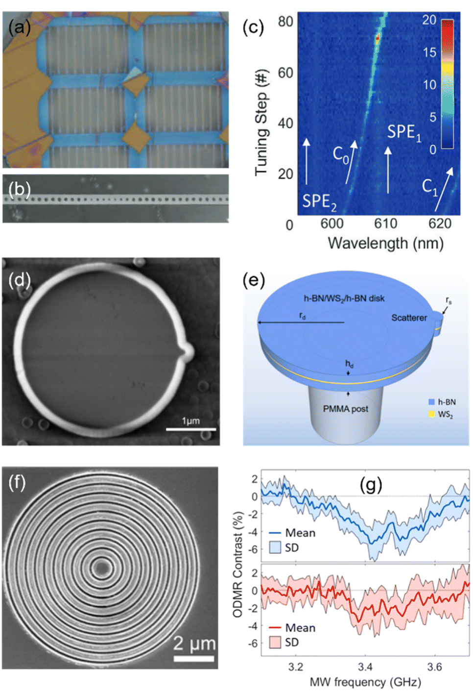 | ||
| Fig. 3 2D material optical cavities. (a) Optical microscope image of the hBN cavity array.13 (b) SEM image of a single freestanding photonic crystal cavity.13 (c) The series of spectra as the temperature increases.13 Copyright 2021 Wiley-VCH GmbH. (d) SEM image of hBN/WS2/hBN microdisk.14 (e) A schematic of microdisk cavity.14 Copyright 2018 American Chemical Society. (f) An SEM image of an hBN bullseye cavity.15 (g) ODMR spectra of a boron vacancy (VB−) with and without cavity effect.15 Copyright 2021 American Chemical Society. | ||
Whispering Gallery Modes (WGM) from 2D material optical cavities have been reported as well. In 2018, a microdisk made of WS2 and hBN was demonstrated and a SEM image of the microdisk is shown in Fig. 3d.14 In this work, a monolayer WS2 serves as a light emitting material, which is sandwiched by two hBN flakes, as schematically depicted in Fig. 3e. They achieved a Q factor of 1200. In contrast to previous research that transferred 2D materials on top of the cavity, this work incorporated a 2D monolayer in the center of the cavity, thereby achieving efficient light–matter coupling. This work also highlighted that this approach is ideal for trion coupling as the ratio of trion PL to exciton PL ratio increases when WS2 is on a hBN substrate.
A monolithic ring resonator made of hBN with an optical Q-factor of 500 was demonstrated in 2019.6 Later, circular Bragg grating cavities were also explored using hBN achieving a Q-factor of 100.15 In this work, the hBN quantum emitters were coupled to the cavity mode and increased optically detected magnetic resonance (ODMR) contrast was observed, as seen in Fig. 3g.
Lasing from 2D materials has been reported in several papers. Until recently, the majority of works on lasing were demonstrated using optical cavities made from conventional 3D bulk materials.16 However, 2D heterostructures can be beneficial in several ways. It is shown that a TMD monolayer exhibits a narrow linewidth when encapsulated by hBN due to efficiently suppressed inhomogeneous broadening.17 In their work, PL spectra of MoSe2, WSe2, MoS2 and WS2 were tested at 300 K and 4 K on SiO2 and capped with hBN, respectively. Additionally, interlayer exciton from 2D heterostructures provide a rich study environment since they alter band structures and exciton states. Interlayer exciton lasers were demonstrated using WSe2 and MoSe2 stacked layers as a gain medium and a silicon nitride grating structure as a cavity.18 This work observed extended spatial coherence of interlayer emission. In 2022, room temperature lasing from monolithic 2D materials was demonstrated for the first time.19 This paper reported indirect bandgap lasing from WS2 disks.
2.4 2D material Mie resonators and metasurface
Mietronics attracted considerable attention as a new platform capable of capturing light in a subwavelength resonator.24,25 Mie resonance occurs when the resonant wavelength approaches the spatial dimension of the resonator, i.e., 2R ≈ λ/n.25 Here R is the radius of the resonator or nanoparticle, and n is the refractive index. Therefore, 2D materials with an unusually high refractive index can aid in the observation of strong Mie resonance. The first Mie resonator from a 2D material was created using WS2.20 The high refractive index of WS2 is advantageous to confine light in a sub-wavelength sized resonator. The in-plain refractive index of the resonator material is larger than 4 in the visible wavelength range. WS2 nanodisks with a varying radius are shown in Fig. 4a, as well as their corresponding scattering spectra (Fig. 4b). In the scattering spectrum, the resonance dip in the scattering spectra arises from anapoles. Effective light–matter coupling in Mie resonator allows the observation of a strong coupling between an anapole and an exciton polariton.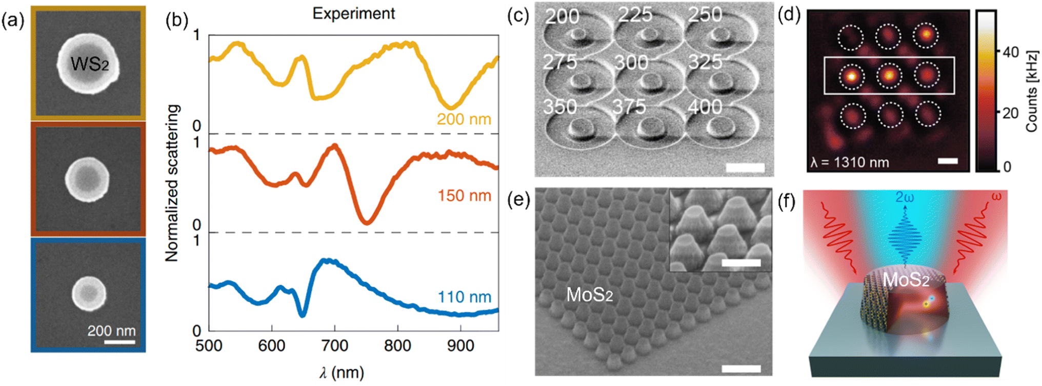 | ||
| Fig. 4 2D material Mie resonators. (a) SEM images of WS2 nanodisks with radii 200 nm, 150 nm, and 110 nm from top to bottom.20 (b) Experimental dark-field scattering data.20 Copyright 2019 Springer Nature Limited. (c) SEM image of fabricated WS2 resonators with varying radii spanning from 200 nm to 400 nm.21 (d) SH intensity map of the disks in (c).21 Copyright 2020 American Chemical Society. (e) EM image of the fabricated MoS2 metasurface.22 (f) Schematic of a MoS2 nanoresonator.23 Copyright 2022 Wiley-VCH GmbH. | ||
Mie-type resonance in a high refractive index 2D material has also been used to enhance nonlinear emission. TMDs exhibit thickness-dependent nonlinear optical responses, and the second harmonic (SH) intensity decreases as the number of layers increases.26 To increase the nonlinearity of TMDs, various external optical/plasmonic cavities were implemented. Fig. 4c demonstrates the direct creation of nanoresonators on WS2 to improve the second harmonic generation.21 Patterned WS2 discs display anapole-like resonance behaviour, which boosts SH generation resonantly. To test Mie-resonance enhanced SH, disks with varied radii were fabricated as shown in Fig. 4c. Fig. 4d shows a scanned SH intensity image across the sample. As predicted from simulation, the disk with a radius of around 275 nm exhibits brighter SH emission, due to the anapole mode. These stand-alone TMDs resonators reduce the fabrication complexity.
Light–matter interaction in 2D material metasurface became popular in recent years.27,28 Periodic nanostructures made from MoS2 are reported (Fig. 4d)22 in 2021 and the structure is used for SH and third harmonic (TH) generation. In this paper, tunable SH emission direction, either forwards or backwards, was achieved by varying the excitation wavelength, which selects a different multipolar resonance. In addition, the aspect ratio of the truncated cone structure provides extra degree of freedom and enables directionality control. In 2022, MoS2 disks were fabricated to couple Mie-type resonances to MoS2's C-exciton resonance to enhance SHG intensity.23 Schematic of the MoS2 resonator is shown in Fig. 4f where pump radiation excites the Mie resonance at half of the exciton resonance of the quadratic susceptibility.
A lasing action has been demonstrated using Mie resonance with halide perovskite (CsPbBr3) nanocubes.29 The nanocube in this study has a refractive index of 2.5 and is supported by a sapphire substrate with a refractive index. With TMDs, the index contrast can be improved, and a Mie laser for all 2D materials can possibly be achieved in the near future. Another unexplored area is the region where the resonator is surrounded by a medium with a higher refractive index.25 The majority of research in Mietronics with 2D materials investigated the conventional Mie problem where the resonator has high indices of refraction. The Mie void mode can also be investigated using 2D materials.
In addition, the bulk WS2 on silica was patterned into metasurfaces which support photonic bound states in the continuum (BICs) resonance.30 This work achieved a strong coupling of light–matter interaction, observing a Rabi splitting of 116 meV. hBN metasurfaces were also fabricated demonstrating a sharp BIC resonance with Q-factors above 300.31
3 Perspective and discussion
In recent years, all-2D material integrated photonics, in which all photonic components are made exclusively from 2D materials, has been envisioned. In the majority of cases, a high refractive index is crucial and presents unique opportunities for 2D material devices. Since exfoliated single crystalline 2D materials have been used in many experiments, optical constants from exfoliated 2D materials must be measured experimentally. However, in the past, optical constants were measured from non-crystallin materials, which did not provide a complete set of optical constants for in-plane and out-of-plane. The in-plane and out-of-plane refractive indices of hBN were determined experimentally and revealed significant optical anisotropy.32 In 2022, the optical constants of numerous 2D materials were measured in the 300–1700 nm range. They studied WS2, WSe2, MoS2, MoSe2, MoTe2, ReS2, WTe2, TaS2, TaSe2 and NbSe2.33 The paper reported high refractive indices over 4 from MoS2, MoSe2 and MoTe2. Birefringence over 1 was observed from MoS2, MoSe2, WS2, WSe2 and ReS. Large optical anisotropy is particularly essential since it underlies the functionality of many optical devices, such as polarizers, waveplates, and so on, and it enables more compact and efficient devices.34 All-2D material integrated nanophotonics is envisioned as a result of the recent interest in such 2D-based optical systems.35,36 Light will be absorbed, contained, guided, and detected by an all-2D integrated chip. All-2D devices can provide a reduced footprint, greater energy efficiency, and enhanced light–matter interactions.35 Unique optical phenomena of 2D materials, such as interlayer exciton, Moire excitons, and valley-dependent exciton, may incorporated into all-2D photonics devices in the future. Although nanofabrication and CVD growth of 2D materials need to improve further, the manipulation of chemical and physical properties of 2D materials has been developed dramatically in recent years.37 Overall, photonic devices made of 2D materials will benefit from this rich research environment.Conflicts of interest
There are no conflicts to declare.References
- R. Mas-Balleste, C. Gomez-Navarro, J. Gomez-Herrero and F. Zamora, 2D materials: to graphene and beyond, Nanoscale, 2011, 3, 20–30 RSC.
- Z. Wang, et al., Two-dimensional light-emitting materials: preparation, properties and applications, Chem. Soc. Rev., 2018, 47, 6128–6174 RSC.
- X. Zhang, et al., Guiding of visible photons at the angstrom thickness limit, Nat. Nanotechnol., 2019, 14, 844–850, DOI:10.1038/s41565-019-0519-6.
- S. Kim, et al., Photonic crystal cavities from hexagonal boron nitride, Nat. Commun., 2018, 9, 1–8 CrossRef PubMed.
- J. Lynch, L. Guarneri, D. Jariwala and J. van de Groep, Tutorial: Exciton Resonances for Atomically-Thin Optics, arXiv, 2022, preprint arXiv:2206.12175 Search PubMed.
- J. E. Fröch, Y. Hwang, S. Kim, I. Aharonovich and M. Toth, Photonic nanostructures from hexagonal boron nitride, Adv. Opt. Mater., 2019, 7, 1801344 CrossRef.
- C. Li, et al., Integration of hBN quantum emitters in monolithically fabricated waveguides, ACS Photonics, 2021, 8, 2966–2972 CrossRef CAS.
- J. B. Khurgin, Two-dimensional exciton–polariton—light guiding by transition metal dichalcogenide monolayers, Optica, 2015, 2, 740–742 CrossRef CAS.
- S.-H. Gong and Q.-H. Park, Gyroelectric guided modes with transverse optical spin, Opt. Express, 2021, 29, 10631–10638 CrossRef PubMed.
- H. Yang, et al., Optical waveplates based on birefringence of anisotropic two-dimensional layered materials, ACS Photonics, 2017, 4, 3023–3030 CrossRef CAS.
- C.-H. Liu, et al., Ultrathin van der Waals metalenses, Nano Lett., 2018, 18, 6961–6966 CrossRef CAS PubMed.
- H. Lin, et al., Diffraction-limited imaging with monolayer 2D material-based ultrathin flat lenses, Light: Sci. Appl., 2020, 9, 1–11 CrossRef PubMed.
- J. E. Fröch, et al., Purcell Enhancement of a Cavity-Coupled Emitter in Hexagonal Boron Nitride, Small, 2022, 18, 2104805 CrossRef PubMed.
- T. Ren, P. Song, J. Chen and K. P. Loh, Whisper gallery modes in monolayer tungsten disulfide-hexagonal boron nitride optical cavity, ACS Photonics, 2018, 5, 353–358 CrossRef CAS.
- J. E. Fröch, et al., Coupling spin defects in hexagonal boron nitride to monolithic bullseye cavities, Nano Lett., 2021, 21, 6549–6555 CrossRef PubMed.
- L. Reeves, Y. Wang and T. F. Krauss, 2D material microcavity light emitters: to lase or not to lase?, Adv. Opt. Mater., 2018, 6, 1800272 CrossRef.
- F. Cadiz, et al., Excitonic linewidth approaching the homogeneous limit in MoS 2-based van der Waals heterostructures, Phys. Rev. X, 2017, 7, 021026 Search PubMed.
- E. Y. Paik, et al., Interlayer exciton laser of extended spatial coherence in atomically thin heterostructures, Nature, 2019, 576, 80–84 CrossRef CAS PubMed.
- J. Sung, et al., Room-temperature continuous-wave indirect-bandgap transition lasing in an ultra-thin WS2 disk, Nat. Photonics, 2022, 16, 792–797 CrossRef CAS.
- R. Verre, et al., Transition metal dichalcogenide nanodisks as high-index dielectric Mie nanoresonators, Nat. Nanotechnol., 2019, 14, 679–683, DOI:10.1038/s41565-019-0442-x.
- S. Busschaert, et al., Transition metal dichalcogenide resonators for second harmonic signal enhancement, ACS Photonics, 2020, 7, 2482–2488 CrossRef CAS.
- M. Nauman, et al., Tunable unidirectional nonlinear emission from transition-metal-dichalcogenide metasurfaces, Nat. Commun., 2021, 12, 1–11 CrossRef PubMed.
- A. A. Popkova, et al., Nonlinear Exciton-Mie Coupling in Transition Metal Dichalcogenide Nanoresonators, Laser Photonics Rev., 2022, 2100604 CrossRef CAS.
- K. Koshelev and Y. Kivshar, Dielectric resonant metaphotonics, ACS Photonics, 2020, 8, 102–112 CrossRef.
- Y. Kivshar, The Rise of Mie-tronics, ACS Publications, 2022, vol. 22, pp. 3513–3515 Search PubMed.
- H. G. Rosa, et al., Characterization of the second-and third-harmonic optical susceptibilities of atomically thin tungsten diselenide, Sci. Rep., 2018, 8, 1–7 CAS.
- S. So, J. Mun, J. Park and J. Rho, Revisiting the Design Strategies for Metasurfaces: Fundamental Physics, Optimization, and Beyond, Adv. Mater., 2022, 2206399 CrossRef PubMed.
- G. Yoon, T. Tanaka, T. Zentgraf and J. Rho, Recent progress on metasurfaces: applications and fabrication, J. Phys. D: Appl. Phys., 2021, 54, 383002 CrossRef CAS.
- E. Tiguntseva, et al., Room-temperature lasing from Mie-resonant nonplasmonic nanoparticles, ACS Nano, 2020, 14, 8149–8156 CrossRef CAS PubMed.
- T. Weber, et al., Strong light-matter interaction with self-hybridized bound states in the continuum in monolithic van der Waals metasurfaces, arXiv, 2022, preprint arXiv:2209.01944 Search PubMed.
- L. Kühner, et al., High-Q Nanophotonics over the Full Visible Spectrum Enabled by Hexagonal Boron Nitride Metasurfaces, arXiv, 2022, preprint arXiv:2210.11314 Search PubMed.
- Y. Rah, Y. Jin, S. Kim and K. Yu, Optical analysis of the refractive index and birefringence of hexagonal boron nitride from the visible to near-infrared, Opt. Lett., 2019, 44, 3797–3800 CrossRef CAS PubMed.
- B. Munkhbat, P. Wróbel, T. J. Antosiewicz and T. O. Shegai, Optical Constants of Several Multilayer Transition Metal Dichalcogenides Measured by Spectroscopic Ellipsometry in the 300–1700 nm Range: High Index, Anisotropy, and Hyperbolicity, ACS Photonics, 2022, 9, 2398–2407 CrossRef CAS PubMed.
- G. Ermolaev, et al., Giant optical anisotropy in transition metal dichalcogenides for next-generation photonics, Nat. Commun., 2021, 12, 1–8 CrossRef PubMed.
- H. Ling, R. Li and A. R. Davoyan, All van der Waals integrated nanophotonics with bulk transition metal dichalcogenides, ACS Photonics, 2021, 8, 721–730 CrossRef CAS.
- B. Munkhbat, B. Küçüköz, D. G. Baranov, T. J. Antosiewicz and T. O. Shegai, Nanostructured Transition Metal Dichalcogenide Multilayers for Advanced Nanophotonics, arXiv, 2022, preprint arXiv:2202.04898 Search PubMed.
- H. Lin, et al., Engineering van der Waals materials for advanced metaphotonics, Chem. Rev., 2022, 122, 15204–15355 CrossRef CAS PubMed.
| This journal is © The Royal Society of Chemistry 2023 |