
 Open Access Article
 This Open Access Article is licensed under a
 Creative Commons Attribution 3.0 Unported Licence
Transition metal doped pyrite (FeS2) thin films: structural properties and evaluation of optical band gap energies†
Sadia
Khalid
abc,
Mohammad Azad
Malik
*ad,
David J.
Lewis
ad,
Punarja
Kevin
d,
Ejaz
Ahmed
b,
Yaqoob
Khan
c and
Paul
O'Brien
ad
aSchool of Materials, The University of Manchester, Oxford Road, Manchester, M13 9PL, UK. E-mail: azad.malik@manchester.ac.uk; Fax: +44 (0)161 275 4616; Tel: +44 (0)161 275 4652
bDepartment of Physics, Bahauddin Zakariya University, Multan 60800, Pakistan
cNano Science & Catalysis Division, National Centre for Physics, Shahdra Valley Road Quaid-i-Azam University Campus, Islamabad 45320, Pakistan
dSchool of Chemistry, The University of Manchester, Oxford Road, Manchester, M13 9PL, UK
First published on 30th October 2015
Abstract
Iron pyrite (FeS2) is a semiconductor comprised of earth-abundant elements and has the potential to be a low cost photovoltaic material with comparatively low toxicity. The properties of transition metal doped iron pyrite thin films (MxFe1−xS2 where M = Co, Ni, Cu, or Zn) deposited by aerosol-assisted chemical vapour deposition (AACVD) on various substrates including glass, (100) silicon and indium tin oxide (ITO) have been studied. Changes in the cubic lattice parameter as well as peak broadening on doping were observed by powder X-ray diffraction (p-XRD) measurements. The structural properties of the transition metal doped pyrite (MxFe1−xS2) depend strongly on the transition metal dopant used and preferred orientation in all films was found to be along the (200) plane. The influence of transition metal doping on the structure and phase transformation was significant in copper doped pyrite thin films. The height-profiling of MxFe1−xS2 films with atomic force microscopy (AFM) displayed smooth surfaces with uniform distribution of particles. Optical studies revealed that there is increment in the bandgap of MxFe1−xS2 thin films which is supported by previous work. There may be contribution from oxidation of the doped pyrite surface in band gap enhancement observed by X-ray photoelectron spectroscopy (XPS). These findings may be important to improve doped pyrite layers for photovoltaic devices.
1. Introduction
Transition metal sulfides have attractive optical properties for photovoltaics, with high extinction coefficients and band gaps commensurate with the solar photon flux. Iron pyrite (or cubic iron disulfide), β-FeS2 (Eg = 0.95 eV; absorption coefficient, α > 105 cm−1@hν > 1.3–1.4 eV, is potentially the most important transition metal sulfide for sustainable energy applications. Due to the inexpensive nature of its constituent elements, pyrite could potentially expand the opportunity for wide-scale deployment of photovoltaic modules.1 The material is also relatively non-toxic compared with other semiconducting materials used in photovoltaic applications. Additionally, pyrite has also found numerous applications in optoelectronic devices,2,3 energy conversion/storage devices,4,5 agriculture,6 biomedical applications7 and extreme pressure additives in formulated oils.8 Organohalide lead(II) perovskites such as methylammonium lead(II) iodide (CH3NH3PbI3)9 have also emerged as light-harvesting semiconductors for thin film solar cells along with copper indium gallium selenide (CIGS),10 copper zinc tin sulfide (CZTS)11 and quantum dot sensitised solar cells such as those based on nanocrystalline cadmium selenide (CdSe).12The ternary chalcogenides of chalcopyrite type structure (CuInS2, CuGaS2, CuInSe2 or CuGaSe2)13,14 are excellent solar harvesters and highly efficient counter electrodes in dye/quantum dot sensitized solar cells.15 However, many of these materials suffer from potential barriers to mass commercialisation either from toxicity issues (heavy metals such as lead and cadmium), stability to humidity or from the scarcity of one or more of their constituent elements in the Earth's crust.
Pyrite-based photovoltaic devices display low power conversion efficiencies (only up to ca. 3%) that are generally attributed to surface defects which cause low open circuit voltages (VOC).16 Different strategies have been employed for improvement of photovoltaic properties of pyrite17 including bandgap tuning by doping/alloying18 and by fabrication of pyrite composites.8 Sun et al. have investigated from first principles density-functional theory (DFT) calculations that the band gap of pyrite can be increased slightly by cation substitution with ruthenium (Ru) or osmium (Os) to form materials Fe1−xRuxS2 and Fe1−xOsxS2 but their incorporation into pyrite is limited by the large positive enthalpy of mixing.19 Engineering the band gap of pyrite materials by doping potentially makes it possible to produce pyrite photovoltaic devices which utilise architectures based on combinations of wide to narrow bandgaps to increase the power conversion efficiency by capturing more of the solar spectrum.
We have reported the synthesis of single source precursors and their use to deposit semiconductor thin films or nanoparticles.20–27 Recently we reported the aerosol-assisted chemical vapour deposition (AACVD) of a range of materials pertinent to photovoltaic applications, including the organic lead halide perovskite methylammonium lead(II) bromide28 copper sulphide, copper indium sulphide,14 and tin sulphide,29,30 iron selenide31 and, significantly, transition metal doped iron sulphide.32 In this paper we report on structural and surface properties of transition metal (M = Co, Ni, Cu, Zn) doped pyrite (MxFe1−xS2) thin films as well as fully evaluating the effect of doping on the optical band gap energy.
2. Experimental
2.1. Synthesis of precursors (1–5) and deposition of (MxFe1−xS2 where M = Co, Ni, Cu, or Zn) thin films
Transition metal diethyldithiocarbamato complexes (1), [Co(S2CNEt2)3] (2), [Ni(S2CNEt2)2] (3), [Cu(S2CNEt2)2] (4) and [Zn(S2CNEt2)2] (5) were prepared and used to deposit MxFe1−xS2 (where M = Co, Ni, Cu, Zn) thin films by AACVD as described previously32 onto glass, Si(100) and ITO-coated glass. In a typical deposition, 0.3 g (0.6 mmol) of the iron precursor (1) and varying concentration of the dopant precursors (2–5) (0.05 mol%, 0.1 mol%, 0.15 mol%, 0.20 mol%, 0.25 mol%, 0.30 mol%) were used.2.2. Deposition of thin films
Thin films were deposited using AACVD. Glass, silicon or ITO coated glass slides (1 × 2 cm) were used as substrates for the deposition. Substrates were thoroughly cleaned and sonicated in acetone for 30 minutes to remove any possible contamination. In a typical deposition experiment, precursor complex (or a suitable combination of precursors) was dissolved in 15 mL toluene taken in a two-necked 100 mL round-bottom flask. The flask was then connected with an argon gas inlet which passed through the solution and carried the aerosols generated by a PIFCO ultrasonic humidifier to the reactor tube connected to other neck of the flask and placed in a Carbolite furnace. The argon flow rate was controlled at 180 sccm by a Platon flow gauge. Thermolysis of the precursor at the hot substrate surface due to thermally induced reactions led to deposition onto the substrates.2.3. Characterization of thin films
p-XRD studies were performed on an Xpert diffractometer using Cu-Kα radiation (λ = 1.5406 Å). The samples were mounted flat and scanned between 2θ = 25° and 65° with a step size of 0.02°. AFM was carried using a Bruker multimode 8 atomic force microscope operating in Peakforce QNM mode, using a silicon nitride tip. Raman spectroscopy was performed using a Renishaw 1000 microscope system equipped with a 50× objective, with solid-state laser excitation (514.5 nm, 25% power). The incident light was linearly polarised in the sample plane with scattered light left un-analysed for collection by the air cooled CCD. XPS spectra were recorded using a Kratos Axis Ultra spectrometer. Optical measurements were performed at room temperature using Perkin Elmer Lambda 950 UV/Vis/NIR spectrophotometer in the wavelength range 200–1200 nm. Photoluminescence spectra were measured using an Edinburgh Instruments FLS920 spectrofluorimeter. Band gap energies were calculated from the obtained absorbance spectra.3. Results and discussion
3.1. Optical band gaps of doped pyrite films
The optical band gap of pyrite thin films deposited at 350 °C using precursor (1) by AACVD were determined from absorbance measurements by Tauc plots (Fig. S1–S4, ESI†). The indirect bandgap for pyrite thin films was calculated as Eg = 0.92 eV (Fig. S5, ESI†) which is in accordance with the previously reported bandgap value (Eg ≈ 0.95 eV). Band gap studies revealed the improvement in band gap values as well as in absorption coefficient in transition metal doped pyrite (MxFe1−xS2) thin films. The optical spectra of as-deposited films using precursors (1) and varying concentration of the dopant precursors of (2–5) (0.05 mol%, 0.1 mol%, 0.15 mol%, 0.20 mol%, 0.25 mol%, 0.30 mol%) were studied by UV-Vis-NIR spectroscopy. Absorption spectra reveal shifts in the absorption edges by transition metal doping. The energy of the optical bandgap (Eg) was estimated using Tauc plots by plotting energy (E = hν) versus (αhν)n where n = 2 and 1/2 are used to fit the linear regions of the curve for direct and indirect transitions respectively. Extrapolation of the linear portion of the curve to the x-axis ordinate gives the energy of the band gap. The variation in optical band gap energy versus the mole percent of transition metal precursors in the delivery mixture for all dopants is shown in Fig. 1.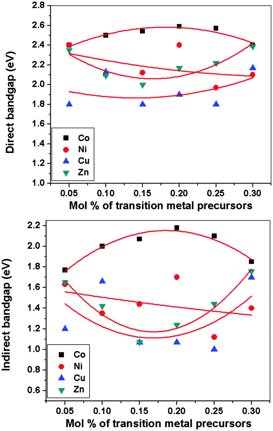 | ||
| Fig. 1 Direct and indirect optical bandgaps vs. mol% of transition metal precursors for doped iron sulphide MxFe1−xS2 thin films (where M = Co, Ni, Cu, Zn) deposited at 350 °C on glass substrates synthesized by AACVD from complexes (1) in combination with (2), (3), (4) and (5). | ||
Cobalt doped pyrite (CoxFe1−xS2) thin films were deposited at 350 °C by AACVD using precursors (1) and varying the concentration of (2). The evaluated direct energy band gaps are: 2.40 eV (0.05 mol%), 2.50 eV (0.10 mol%), 2.54 eV (0.15 mol%), 2.59 eV (0.20 mol%), 2.57 eV (0.25 mol%), and 2.40 eV (0.30 mol%). The evaluated indirect transitions are: 1.77 eV (0.05 mol%), 2.00 eV (0.10 mol%), 2.07 eV (0.15 mol%), 2.18 eV (0.20 mol%), 2.10 eV (0.25 mol%), and 1.85 eV (0.30 mol%) (Fig. S6, ESI†). The blue shift in optical absorption band edge of films suggests the formation of solid solution.33 A similar behaviour has been noted by other laboratories.34,35
The nickel doped pyrite (NixFe1−xS2) thin films were deposited at 350 °C by AACVD using precursors (1) and varying the concentration of (3). The direct optical band gap (Eg) of nickel doped pyrite (NixFe1−xS2) thin films are: 2.40 eV (0.05 mol%), 2.10 eV (0.10 mol%), 2.12 eV (0.15 mol%), 2.40 eV (0.20 mol%), 1.97 eV (0.25 mol%), and 2.10 eV (0.30 mol%). The evaluated indirect transitions are: 1.67 eV (0.05 mol%), 1.35 eV (0.10 mol%), 1.44 eV (0.15 mol%), 1.70 eV (0.20 mol%), 1.12 eV (0.25 mol%), and 1.40 eV (0.30 mol%) (Fig. S7, ESI†). The variation in band gap is linear with varying concentration of dopant precursor for NixFe1−xS2 thin films which indicates the gradual incorporation of nickel within pyrite. The blue shift in optical absorption band edge of films confirms the formation of solid solution.36
The copper doped pyrite (CuxFe1−xS2) thin films were deposited by AACVD at 350 °C using precursors (1) and varying the concentration of (4). The evaluated direct energy band gaps are: 1.80 eV (0.05 mol%), 2.13 eV (0.10 mol%), 1.80 eV (0.15 mol%), 1.90 eV (0.20 mol%), 1.80 eV (0.25 mol%), and 2.17 eV (0.30 mol%). The evaluated indirect transitions are: 1.20 eV (0.05 mol%), 1.66 eV (0.10 mol%), 1.07 eV (0.15 mol%), 1.07 eV (0.20 mol%), 1.00 eV (0.25 mol%), and 1.70 eV (0.30 mol%) (Fig. S8, ESI†). The blue shift in optical absorption band edge of films shows formation of solid solution.37 The band gap varies in CuxFe1−xS2 thin films with concentration of the dopant precursor but less than cobalt due to limited solubility.19
The zinc doped pyrite (ZnxFe1−xS2) thin films were deposited by AACVD at 350 °C using precursors (1) and varying the concentration of (5). The evaluated direct energy band gaps are: 2.35 eV (0.05 mol%), 2.09 eV (0.10 mol%), 2.00 eV (0.15 mol%), 2.17 eV (0.20 mol%), 2.22 eV (0.25 mol%), and 2.39 eV (0.30 mol%). The evaluated indirect transitions are: 1.65 eV (0.05 mol%), 1.42 eV (0.10 mol%), 1.07 eV (0.15 mol%), 1.24 eV (0.20 mol%), 1.44 eV (0.25 mol%), and 1.76 eV (0.30 mol%) (Fig. S9, ESI†). The blue shift in optical absorption band edge of films shows formation of solid solution. The enhancement in band gap of ZnxFe1−xS2 thin films is supported by previous observations.38 Alloying pyrite with different elements involves issues like differences in electronegativity, size, band gap bowing and miscibility.19 Band gap bowing effect was observed in FexM1−xS2 thin films. Increment in the band gap of FexM1−xS2 thin films was observed, which might be attributed to transition metal doping, oxygen alloying and quantum confinement effects.18 Recently, first principle calculations investigated by Xiao et al. explored that biaxial strain can also increase band gap of pyrite.39
3.2. Photoluminescence of doped pyrite films
Photoluminescence (PL) emission spectroscopy can probe band gap energy, impurities and defects within films, and surface structure. Radiative PL emission originates from exciton recombination, where an excited electron recombines with a hole, releasing a photon in the process. High PL quantum yields indicate higher recombination rate of the electron–hole pairs and the lifetime of the photoluminescent state is short.40 Steady state PL measurements for transition metal doped pyrite (MxFe1−xS2) thin films deposited on glass substrates at 350 °C by AACVD was performed at an excitation wave length of 375 nm at ambient temperature.The PL spectra of the cobalt doped pyrite (CoxFe1−xS2) thin films deposited at 350 °C using precursors (1) and varying the concentration of (2) (0.05 mol%, 0.1 mol%, 0.15 mol%, 0.20 mol%, 0.25 mol%, 0.30 mol%) show broad emission peaks in the range of 400–600 nm at different dopant concentration (Fig. S10, ESI†). The emission peaks strongly support band-to-band transitions, which occurs due to exciton recombination of the excited electron in the conduction band with a hole in the valence band. Small features between 550–675 nm are attributed to excitonic peaks in sample at dopant concentration of 0.05 mol%.
Nickel doped pyrite (NixFe1−xS2) thin films deposited at 350 °C using precursors (1) and varying concentration of (3) (0.00 mol%, 0.05 mol%, 0.1 mol%, 0.15 mol%, 0.20 mol%, 0.25 mol%, 0.30 mol%) show broad emission peaks between 389–400 nm for all samples (Fig. S11, ESI†). Small peaks at 500–700 nm might be attributed to the excitonic peaks due to defect states in sample at dopant concentration of 0.15 mol%. PL peak intensity decreases with the increase in nickel doping concentration corresponding to low recombination rates at higher nickel impurity level.
Copper doped pyrite (CuxFe1−xS2) thin films deposited at 350 °C using precursors (1) and varying concentration of (4) (0.05 mol%, 0.1 mol%, 0.15 mol%, 0.20 mol%, 0.25 mol%, 0.30 mol%) show broad emission peaks in the range of 390–400 nm (Fig. S12, ESI†). The zinc doped pyrite (ZnxFe1−xS2) thin films deposited at 350 °C using precursors (1) and varying concentration of (5) (0.05 mol%, 0.1 mol%, 0.15 mol%, 0.20 mol%, 0.25 mol%, 0.30 mol%) showed broad emission peaks in the range of 400–415 nm Fig. S13, ESI†). A similar behaviour was observed in pyrite composites or heterostructures.2,17
3.3. Structural studies
Microstrain and dislocations in the crystal lattice of FeS2 can have an influence upon the band gap of the material. Analysis of peak shifts or peak broadening in the powder X-ray diffraction (p-XRD) patterns of doped pyrite provides a quantification of lattice strain that is a measure of change in lattice constants attributable to crystal imperfections, such as dislocation. Strain may also emerge from crystallite size reduction and alloying.41 The average lattice constant can also be determined from interplanar spacing dhkl: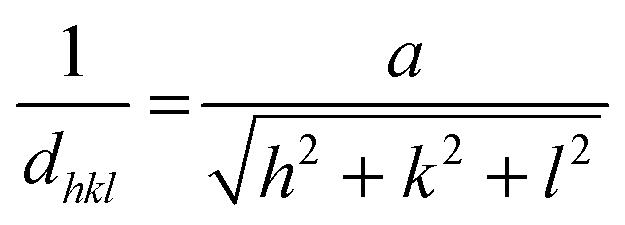 | (1) |
 | (2) |
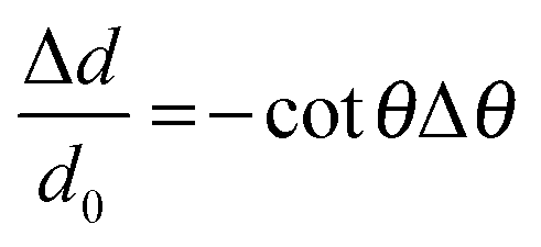
The effect of lattice strain on diffraction peak position varies from peak shifting (uniform strain) to peak broadening (non-uniform strain). A change in the interplanar spacing (Δd) shifts the diffraction peaks toward lower or higher angle resulting a change in the Bragg angle (Δθ). Lattice strain can be expressed as:
 | (3) |
 | (4) |
 | (5) |
 | (6) |
 | (7) |
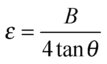
p-XRD analysis of MxFe1−xS2 thin films deposited at 350 °C reveals that the diffraction peaks shift gradually towards lower 2θ values as compared to pyrite with preferred orientation along the (200) plane.32 The doping induces the lattice strain in MxFe1−xS2 thin films. The lattice parameter for the cubic doped films increases monotonically with doping and consequently induces microstrain in cubic structure of pyrite. The average value of microstrain was found to be least in the copper doped while the most in zinc doped pyrite thin films (Table 1). For all doped films, the microstrain values are higher than undoped FeS2 (3.031 × 10⁻³) which is caused by cation substitution that is in good agreement to previously reported values 3.4 × 10⁻³ to 3.4 × 10⁻⁴ for pyrite thin films calculated by Rietveld refinements of X-ray diffraction data.44 Lattice distortion is caused by the difference in sizes the two metal ions into the pyrite lattice. Specifically, the microstrain caused by transition metal doping is proportional to dislocation density. Undoped pyrite thin films on glass substrates, which have a dislocation density of 1.075 × 10⁻³ nm−2 calculated by using eqn (7).
| x | CoxFe1−xS2 | NixFe1−xS2 | CuxFe1−xS2 | ZnxFe1−xS2 | |
|---|---|---|---|---|---|
| a Phase transformation from cubic pyrite to tetragonal chalcopyrite. | |||||
| Lattice constant, (a, nm) | 0.05 | 0.5419 | 0.5425 | 0.5428 | 0.5421 |
| 0.10 | 0.5422 | 0.5427 | 0.5434 | 0.5422 | |
| 0.15 | 0.5424 | 0.5422 | 0.5430 | 0.5421 | |
| 0.20 | 0.5425 | 0.5424 | 0.5432 | 0.5422 | |
| 0.25 | 0.5430 | 0.5426 | 0.5435 | 0.5421 | |
| 0.30 | 0.5444 | 0.5425 | 0.4177a | Amorphous | |
| Microstrain, (ε) ×10−3 | 0.05 | 3.147 | 3.542 | 3.606 | 4.179 |
| 0.10 | 3.588 | 4.730 | 3.335 | 3.391 | |
| 0.15 | 2.508 | 3.032 | 2.995 | 3.852 | |
| 0.20 | 2.992 | 2.577 | 3.056 | 4.817 | |
| 0.25 | 3.633 | 2.756 | 2.982 | 3.866 | |
| 0.30 | 4.125 | 3.991 | 3.372 | Amorphous | |
| Dislocation density, (δ, nm−2) ×10−3 | 0.05 | 1.404 | 1.280 | 1.416 | 1.819 |
| 0.10 | 2.770 | 3.158 | 1.063 | 1.295 | |
| 0.15 | 0.667 | 0.088 | 1.252 | 1.682 | |
| 0.20 | 0.080 | 0.082 | 1.048 | 2.083 | |
| 0.25 | 1.263 | 1.120 | 1.786 | 1.584 | |
| 0.30 | 1.799 | 2.557 | 1.190 | Amorphous | |
Divalent cations with ionic radius larger than Fe2+ incorporated into the FeS2 structure form substitutional solid solutions and the lattice parameter should be increased. The lattice parameter ‘a’ of films was calculated using eqn (2) as; 0.5420 nm for undoped FeS2 and 0.5419–0.5444 nm (CoxFe1−xS2), 0.5422–0.5427 nm (NixFe1−xS2), 0.5428–0.5435 nm (CuxFe1−xS2) and 0.5421–0.5422 nm (ZnxFe1−xS2). The increase of the lattice parameter suggests an increase of the interplanar crystal spacing. The average lattice distortion degree was found to be greatest in copper-doped pyrite thin films greater than the values already reported for pyrite thin films where δ < 0.45 The average value of dislocation density was found to be maximum in zinc doped and minimum in copper doped pyrite thin films. The most pronounced structural changes observed with p-XRD was observed in the case of copper-doped pyrite thin films where the lattice changes from cubic (pyrite-ICDD No. 01-073-8127) to tetragonal (chalcopyrite-ICDD No. 01-083-0984) denoted by star in Table 1 as-evidenced by the appearance of a peak at 2θ = 29.5°. This deviation in structural parameters varies from cobalt to zinc doped pyrite thin films. The preferred orientation was along the (200) crystal plane for all dopants except copper doped pyrite thin films where phase transformation from pyrite to chalcopyrite at x = 0.30 mol% develops preferred orientation along the (112) plane. Some diffraction peaks were too weak to be observed at higher concentration of zinc precursor (x = 0.30 mol%) and pattern was observed as for amorphous material.32
The MxFe1−xS2 films deposited by AACVD at 350 °C on indium tin oxide (ITO) substrates were characterized by p-XRD. X-ray patterns of the as-deposited films (Fig. 2) show the cubic pyrite (FeS1.96 (ICDD No. 01-073-8127)) phase. It was possible to index the Bragg reflections to the (111), (200), (210), (220), (311), (222), (023) and (321). The Bragg reflections at 2θ = 30.273° and 35.165° correspond to the (222) and (400) planes respectively for indium tin oxide (ITO) (ICDD ref No. 00-039-1058). The lattice mismatch of doped pyrite thin films from wide bandgap semiconductor and solar substrate indium tin oxide (ITO) was also investigated. Microstrain and dislocation density has a greater value for all the as-deposited MxFe1−xS2 thin films fabricated by AACVD at 350 °C on indium tin oxide (ITO) substrates as compared to glass substrates due to lattice imperfections originating from lattice misfit in the films (Table 2).46 This behaviour is potentially related to small crystallite size on this substrate.44
 | ||
| Fig. 2 p-XRD patterns of reference iron sulfide (pyrite-(ICDD No.01-073-8127)), indium tin oxide (ITO-(ICDD ref No. 00-039-1058)) and transition metal doped pyrite MxFe1−xS2 thin films at x = 0.10 mol% deposited from complexes (1) and (2), (3), (4) and (5) at 350 °C on ITO substrates by AACVD. | ||
| ×10−3 | CoxFe1−xS2 | NixFe1−xS2 | CuxFe1−xS2 | ZnxFe1−xS2 |
|---|---|---|---|---|
| Microstrain (ε) | 6.323 | 4.202 | 4.988 | 4.279 |
| Dislocation density (δ, nm−2) | 3.395 | 2.100 | 2.371 | 2.085 |
Unlike the conventional deposition methods, deposition of undoped and doped pyrite thin films using the solution-based process like aerosol assisted chemical vapour deposition (AACVD) requires the particular molarity of precursor solutions. Additionally, it is challenging to sustain the pyrite phase at the same time while varying dopants under similar experimental conditions. In general, we observed that diethyldithiocarbamato transition metal complexes produced good quality transition metal doped pyrite thin films.
The as-deposited MxFe1−xS2 thin films on the ITO substrate were further characterized by Raman spectroscopy which revealed that the pyrite phase is dominant in all films. The Raman spectrum of CoxFe1−xS2 (x = 0.10 mol%) thin films synthesised by AACVD at 350 °C on indium tin oxide (ITO) substrates (Fig. 3(a)) shows three peaks at 341, 375, and 426 cm−1, which are the characteristic active modes for pyrite (FeS2) corresponding to the S2 dumb bell libration (Eg), S–S in-phase stretch (Ag), and coupled libration and stretch (Tg) modes, respectively.5 We tentatively assign the Raman band at 320 cm−1 to minor marcasite impurities.47–49 The Raman spectrum of NixFe1−xS2 (x = 0.10 mol%) thin films synthesised by AACVD at 350 °C on indium tin oxide (ITO) substrates (Fig. 3(b)) shows three peaks at 339, 375, and 410 cm−1 corresponding to characteristic active modes for pyrite (FeS2). NixFe1−xS2 film shows no Raman band for substrate or marcasite impurity. The Raman spectrum of CuxFe1−xS2 (x = 0.10 mol%) thin films synthesised by AACVD at 350 °C on indium tin oxide (ITO) substrates (Fig. 3(c)) exhibits three peaks at 288, 324, and 361 cm−1 corresponding to characteristic active modes for oxidized pyrite that might be due to long exposure time for film under high energy laser beam for ∼1 min during spectrum capture. The chalcopyrite (CuFeS2) structure exhibit bands at 287, 351 and 470 cm−1.47 Raman spectrum of films on ITO substrate have the expected vibrational modes at 109, 135, 307, 366, 495, 517 and 630 cm−1 assigned to In2O3. The vibrational band at 631 cm−1 in the ITO spectrum is assigned to the contribution of the In–O (vibrational band at 630 cm−1) and the Sn–O (vibrational modes at 633 cm−1). The Sn–O exhibits vibrational modes at 144, 175, 240, 248, 433, 476 and 584 cm−1.50 The Raman spectrum of ZnxFe1−xS2 (x = 0.10 mol%) thin films deposited at 350 °C on indium tin oxide (ITO) substrates (Fig. 3(d)) displays three peaks at 336, 371, and 410 cm−1 corresponding to characteristic active modes for pyrite (FeS2). ZnxFe1−xS2 film shows no Raman band for the substrate or any marcasite impurities.
 | ||
| Fig. 3 Raman spectra of transition metal doped pyrite MxFe1−xS2 thin films at x = 0.10 mol% deposited from complexes (1) and (2), (3), (4) and (5) at 350 °C on ITO substrate deposited by AACVD. | ||
These observations demonstrate that all transition metal doped pyrite thin films MxFe1−xS2 are cubic for all dopants except copper. This observation might be related to the miscibility of the respective sulfide of the transition metal complex at specific deposition temperature and dopant concentration conditions. Consequently, cation substitution in pyrite causes structural transformation and lattice strain.51 Also, extended laser irradiation (>500 s) in air induces the substitution of sulfur by oxygen in the chalcogenide materials and the subsequent formation of transition metal oxides during Raman measurement.
3.4. Surface properties
The as-deposited transition metal doped pyrite (MxFe1−xS2) thin films were characterized using atomic force microscopy (AFM) to explore their surface topography and morphology. Selective MxFe1−xS2 thin films deposited on glass substrates at 350 °C by AACVD using precursors (1) and varying concentration of the dopant precursors of (2–5) were imaged by AFM (Fig. 4). The morphology of MxF1−xS2 thin films depends on dopant concentration as well as on transition metal complex that is used as single source precursor. Overall surface morphology of thin films shows adherent, compact and crack/fracture free surfaces. Adherence is a chemical-physical phenomenon depending on the method of thin film fabrication and the adhesion at nanoscale decreases with increasing surface roughness.52 Thin films fabricated by chemical vapour deposition method are typically adherent. Average roughness values for MxF1−xS2 thin films varied as 13.9 nm, 7.9 nm, 6.8 nm and 6.1 nm. Variation in crystallite size and growth with doping has been discussed previously.32 | ||
| Fig. 4 Height-profile AFM images of transition metal doped pyrite (MxFe1−xS2) thin films deposited at 350 °C on glass substrates by AACVD from complexes (a) (1) and (2) at x = 0.05 mol%, (b) (1) and (4) at x = 0.30 mol%, (c and d) (1) and (5) at x = 0.30 mol%. | ||
Surface analysis of transition metal doped pyrite (MxFe1−xS2) thin films confirms the presence of uniform and crack-free surfaces. Thin film crystalline quality, morphology and texture are associated with surface roughness. The surface roughness in transition metal (Co, Ni, Cu, Zn) doped pyrite (MxFe1−xS2) thin films deviate with dopant concentration and transition metal precursors. Zinc doped pyrite thin films showed the smoothest surfaces. Particle roughness and height profiles were studied using atomic force microscopy (AFM). Fig. 4 shows that the surface texture of the films varies from granular to the spherical growth of the particles in thin films with varying concentration of dopant. Moreover, roughness parameters, skewness (Rsk) and kurtosis (Rku) were calculated from AFM analysis. Positive low values of skewness (Rsk = 0.396, 0843, 0.089, 0.404) display that peaks are somewhat dominant on the films surface while the kurtosis values (Rku = 3.578, 3.307, 2.524, 2.301) indicate that the grain distribution over the scanned area has comparatively few high peaks and low valleys which indicates a slightly undulating surface.53 Surface morphology plays an important role in photovoltaic devices.54 AFM height profiles of transition metal doped pyrite (MxFe1−xS2) thin films show uniform distribution of particles with average particle height 130 nm (Fig. 4). AFM data for scanning areas ranging from 0.5 × 0.5 up to 1 × 1 μm2 for transition metal doped pyrite films revealed smooth surfaces having root mean squared (RMS) roughness values of 18.9 nm, 10.0 nm, 8.3 nm and 7.4 nm (Fig. 4). These smooth films doped with cobalt show microstrain values similar to FeS2 itself and suggests that microstrain may be correlated to the overall smoothness of films grown by AACVD.55
Photoelectron spectroscopy (XPS) was used for qualitative analysis of selected transition metal doped pyrite (MxFe1−xS2) thin films prepared by AACVD using precursors (1) and the dopant precursors (2-5) of concentration 0.30 mol%. Integration and comparison of the Fe 2p, Co 2p, Ni 2p, Cu 2p and Zn 2p signals revealed compositions of transition metal doped pyrite thin films (MxFe1−xS2). XPS analysis (Fig. 5) revealed phase transformation of pyrite to doped pyrite with an approximate surface composition of MxFe1−xS2 (discounting other inconsequential species that may be present).56–58 Copper doped pyrite thin film at x = 0.30 mol% revealed transformation from pyrite (FeS2) to chalcopyrite (CuFeS2) at binding energy 161.3 eV of S 2p3/2 and 74.65 eV for Cu 3p3/2 (Fig. 5).
 | ||
| Fig. 5 XPS spectra of transition metal doped pyrite MxFe1−xS2 thin films at x = 0.30 mol% deposited from complexes (1) and (2), (3), (4) and (5) at 350 °C on glass substrate deposited by AACVD. | ||
Density functional theory (DFT) calculation revealed that the interaction of impure pyrite (impurities like As, Co and Ni) with oxygen can enhance the oxidation of pyrite.59 Pyrite containing impurities observed to be more reactive than un-doped pyrite.60,61 XPS studies of the oxidized transition metal doped pyrite revealed the shifting of binding energies of surface components towards higher binding energies as compared to pure pyrite.56 This observation is in accordance with the results from XPS studies suggesting that bulk defect states introduced in doped pyrite increase the density of occupied surface states which mediate charge transfer and thus oxidation.62
Thus, surface study reveals the influence of doping on oxidation processes related to the surface defects.
Subsequently, pyrite cannot simply be compared with and developed along the line of classical semiconductor compounds. Some structural parameters were qualitatively discussed in the present work, but categorically, further systematic work is required to establish the role of impurities in doped pyrite to improve its properties.
4. Conclusions
Despite their promise, photovoltaic modules containing FeS2 continue to show small photovoltages which have limited power conversion efficiencies to around 3%. Bandgap engineering of pyrite by doping may help in increasing power conversion efficiency by increasing the portion of the solar spectrum absorbed. Transition metal doped iron pyrite (MxFe1−xS2) thin films were deposited on glass and indium tin oxide (ITO) coated glass substrates by AACVD using diethyldithiocarbamato complexes of the general formula [M(S2CN(Et)2)n]. Lattice parameters and optical band gap confirmed the formation of a solid solution as determined by powder X-ray diffraction (p-XRD) and UV-Vis spectroscopy. Raman spectroscopy also helped to identify the phase of films deposited on ITO substrates. Atomic force microscopy (AFM) confirmed crack free surfaces. X-ray photoelectron spectroscopy (XPS) allowed the evaluation of species at the surface MxFe1−xS2 thin films.The structural properties of the transition metal doped pyrite (MxFe1−xS2) depend strongly on the transition metal dopant used. Preferred orientation in all MxFe1−xS2 thin films was observed to be along (200) plane. The influence of transition metal doping on the structure and phase transformation was significant in copper doped pyrite thin films. Optical studies revealed that there is increment in the bandgap of MxFe1−xS2 thin films which is supported by previous work. There may be contribution from oxidation of the doped pyrite surface in band gap enhancement. Most of theoretical studies regarding band gap enhancement of doped pyrite propose that transition metals (Ni,Cu) introduce new defect states within pyrite structure.51 Density functional theory (DFT) calculations show that oxygen alloying in pyrite can increase its band gap 1.0–1.5 eV without introducing electronic states within the bandgap.18 There may be contribution in band gap enhancement from oxygen alloying. Similar results have been reported previously.63
Lattice parameter increases can be correlated with the quantity of the dopant transition metal ion incorporated. The band gap of the MxFe1−xS2 thin films increases with increasing dopant in all cases. Previously, improved photoresponse was observed with zinc alloyed into the ZnxFe1−xS2 nanocrystal photoconductor attributed to the increased band gap.38 Improved optical absorption with transition metal doping was observed in the MxFe1−xS2 thin films engineering the optical bandgap. These may open the opportunities for photovoltaic applications using the MxFe1−xS2 thin films with engineered wider bandgaps than pyrite.
Acknowledgements
SK thanks the Higher Education Commission of Pakistan for an IRSIP scholarship and the POB group (The University of Manchester, United Kingdom) for assistance with this research. SK is also grateful to Nano Science and Catalysis Division (NS&CD), National Centre for Physics (NCP) Islamabad, Pakistan for providing research facilities as hosted researcher. This work was also funded by the UK Engineering and Physical Sciences Research Council (EPSRC) Core Capability in Chemistry grant (EPSRC grant number EP/K039547/1). We thank Dr John Walton (University of Manchester) for performing XPS measurements and Dr Louise Natrajan (University of Manchester) for access to the spectrofluorimeter.References
- C. Wadia, A. P. Alivisatos and D. M. Kammen, Environ. Sci. Technol., 2009, 43, 2072–2077 CrossRef CAS PubMed.
- M. A. Khan, J. Sarker, S. Lee, S. C. Mangham and M. Manasreh, Mater. Chem. Phys., 2014, 148, 1022–1028 CrossRef.
- M. Wang, C. Xing, K. Cao, L. Zhang, J. Liu and L. Meng, J. Mater. Chem. A, 2014, 2, 9496–9505 CAS.
- X. Wen, X. Wei, L. Yang and P. K. Shen, J. Mater. Chem. A, 2015, 3, 2090–2096 CAS.
- M. S. Faber, M. A. Lukowski, Q. Ding, N. S. Kaiser and S. Jin, J. Phys. Chem. C, 2014, 118, 21347–21356 CAS.
- G. Srivastava, C. K. Das, A. Das, S. K. Singh, M. Roy, H. Kim, N. Sethy, A. Kumar, R. K. Sharma, S. K. Singh, D. Philip and M. Das, RSC Adv., 2014, 4, 58495–58504 RSC.
- Y. Bai, J. Yeom, M. Yang, S.-H. Cha, K. Sun and N. A. Kotov, J. Phys. Chem. C, 2013, 117, 2567–2573 CAS.
- M. Zhang, B. Chen, H. Tang, G. Tang, C. Li, L. Chen, H. Zhang and Q. Zhang, RSC Adv., 2015, 5, 1417–1423 RSC.
- H. J. Snaith, J. Phys. Chem. Lett., 2013, 4, 3623–3630 CrossRef CAS.
- A. Chirilă, S. Buecheler, F. Pianezzi, P. Bloesch, C. Gretener, A. R. Uhl, C. Fella, L. Kranz, J. Perrenoud, S. Seyrling, R. Verma, S. Nishiwaki, Y. E. Romanyuk, G. Bilger and A. N. Tiwari, Nat. Mater., 2011, 10, 857–861 CrossRef PubMed.
- D. J. Lewis, P. Kevin, O. Bakr, C. A. Muryn, M. A. Malik and P. O'Brien, Inorg. Chem. Front., 2014, 1, 577–598 RSC.
- D. J. Binks, Phys. Chem. Chem. Phys., 2011, 13, 12693–12704 RSC.
- S. N. Malik, S. Mahboob, N. Haider, M. A. Malik and P. O'Brien, Nanoscale, 2011, 3, 5132–5139 RSC.
- S. N. Malik, A. Q. Malik, R. F. Mehmood, G. Murtaza, Y. G. Alghamdi and M. A. Malik, New J. Chem., 2015, 39, 4047–4054 RSC.
- M. Azad Malik, N. Revaprasadu and K. Ramasamy, Nanomaterials for solar energy, Nanoscience: Volume 1: Nanostructures through Chemistry, The Royal Society of Chemistry, 2013, pp. 29–59 Search PubMed.
- P. Lazić, R. Armiento, F. Herbert, R. Chakraborty, R. Sun, M. Chan, K. Hartman, T. Buonassisi, B. Yildiz and G. Ceder, J. Phys.: Condens. Matter, 2013, 25, 465801 CrossRef PubMed.
- A. Kirkeminde, R. Scott and S. Ren, Nanoscale, 2012, 4, 7649–7654 RSC.
- J. Hu, Y. Zhang, M. Law and R. Wu, J. Am. Chem. Soc., 2012, 134, 13216–13219 CrossRef CAS PubMed.
- R. Sun and G. Ceder, Phys. Rev. B: Condens. Matter Mater. Phys., 2011, 84, 245211 CrossRef.
- N. Revaprasadu, M. A. Malik, P. O'Brien and G. Wakefield, J. Mater. Res., 1999, 14, 3237–3240 CrossRef CAS.
- M. A. Malik, M. Motevalli and P. O'Brien, Inorg. Chem., 1995, 34, 6223–6225 CrossRef CAS.
- M. A. Malik, M. Motevalli, J. R. Walsh and P. O'Brien, Organometallics, 1992, 11, 3136–3139 CrossRef CAS.
- A. A. Memon, M. Afzaal, M. A. Malik, C. Q. Nguyen, P. O'Brien and J. Raftery, Dalton Trans., 2006, 4499–4505 RSC.
- D. Binks, S. Bant, D. West, P. O'Brien and M. Malik, J. Mod. Opt., 2003, 50, 299–310 CAS.
- C. Q. Nguyen, A. Adeogun, M. Afzaal, M. A. Malik and P. O'Brien, Chem. Commun., 2006, 2182–2184 RSC.
- M. A. Malik, M. Motevalli, T. Saeed and P. O'Brien, Adv. Mater., 1993, 5, 653–654 CrossRef CAS; K. Ramasamy, M. A. Malik, N. Revaprasadu and P. O'Brien, Chem. Mater., 2013, 25, 3551–3569 CrossRef.
- A. Panneerselvam, C. Q. Nguyen, M. A. Malik, P. O'Brien and J. Raftery, J. Mater. Chem., 2009, 19, 419–427 RSC.
- D. J. Lewis and P. O'Brien, Chem. Commun., 2014, 50, 6319–6321 RSC.
- P. Kevin, S. N. Malik, M. A. Malik and P. O'Brien, Chem. Commun., 2014, 50, 14328–14330 RSC.
- P. Kevin, D. J. Lewis, J. Raftery, M. Azad Malik and P. O'Brien, J. Cryst. Growth, 2015, 415, 93–99 CrossRef CAS.
- M. Akhtar, M. A. Malik, J. Raftery and P. O'Brien, J. Mater. Chem. A, 2014, 2, 20612–20620 CAS.
- S. Khalid, E. Ahmed, M. Azad Malik, D. J. Lewis, S. Abu Bakar, Y. Khan and P. O'Brien, New J. Chem., 2015, 39, 1013–1021 RSC.
- Y. Tomm, R. Schieck, K. Ellmer and S. Fiechter, J. Cryst. Growth, 1995, 146, 271–276 CrossRef CAS.
- J. Jiao, L. Chen, D. Kuang, W. Gao, H. Feng and J. Xia, RSC Adv., 2011, 1, 255–261 RSC.
- F. Long, J. He, M. Zhang, X. Wu, S. Mo, Z. Zou and Y. Zhou, J. Mater. Sci., 2015, 50, 1848–1854 CrossRef CAS.
- R. Chandler and R. Bene, Phys. Rev. B: Solid State, 1973, 8, 4979 CrossRef CAS.
- I. Ferrer, F. Caballero, C. De las Heras and C. Sánchez, Solid State Commun., 1994, 89, 349–352 CrossRef CAS.
- B. Mao, Q. Dong, Z. Xiao, C. L. Exstrom, S. A. Darveau, T. E. Webber, B. D. Lund, H. Huang, Z. Kang and J. Huang, J. Mater. Chem. A, 2013, 1, 12060–12065 CAS.
- P. Xiao, X.-L. Fan, L.-M. Liu and W.-M. Lau, Phys. Chem. Chem. Phys., 2014, 16, 24466–24472 RSC.
- T. H. Gfroerer, Encyclopedia of Analytical Chemistry, 2000 Search PubMed.
- P. Scardi, M. Leoni and R. Delhez, J. Appl. Crystallogr., 2004, 37, 381–390 CrossRef CAS.
- V. Mote, Y. Purushotham and B. Dole, J. Theor. Appl. Phys., 2012, 6, 1–8 CrossRef.
- P. Chelvanathan, Y. Yusoff, F. Haque, M. Akhtaruzzaman, M. Alam, Z. Alothman, M. Rashid, K. Sopian and N. Amin, Appl. Surf. Sci., 2015, 334, 138–144 CrossRef CAS.
- C. De las Heras, J. de Vidales, I. Ferrer and C. Sánchez, J. Mater. Res., 1996, 11, 211–220 CrossRef CAS.
- L. Y. Huang and L. Meng, Mater. Sci. Eng., B, 2007, 137, 310–314 CrossRef CAS.
- L. Meng, Y. Liu and L. Tian, J. Cryst. Growth, 2003, 253, 530–538 CrossRef CAS.
- S. N. White, Chem. Geol., 2009, 259, 240–252 CrossRef CAS.
- C. Sourisseau, R. Cavagnat and M. Fouassier, J. Phys. Chem. Solids, 1991, 52, 537–544 CrossRef CAS.
- H. Lutz and B. Müller, Phys. Chem. Miner., 1991, 18, 265–268 CrossRef CAS.
- O. M. Berengue, A. D. Rodrigues, C. J. Dalmaschio, A. J. Lanfredi, E. R. Leite and A. J. Chiquito, J. Phys. D: Appl. Phys., 2010, 43, 045401 CrossRef.
- P. Abraitis, R. Pattrick and D. Vaughan, Int. J. Miner. Process., 2004, 74, 41–59 CrossRef CAS.
- R. De Oliveira, D. Albuquerque, F. Leite, F. Yamaji and T. Cruz, Measurement of the nanoscale roughness by atomic force microscopy: basic principles and applications, INTECH Open Access Publisher, 2012 Search PubMed.
- E. S. Gadelmawla, M. M. Koura, T. M. A. Maksoud, I. M. Elewa and H. H. Soliman, J. Mater. Process. Technol., 2002, 123, 133–145 CrossRef; R. Muhammad, A. M. Rana, M. Hafeez, E. Ahmed, A. S. Bhatti, M. F. Wasiq and M. Y. Nadeem, Acta Chim. Slov., 2014, 61, 80–86 Search PubMed.
- C. Teichert and I. Beinik, Conductive atomic-force microscopy investigation of nanostructures in microelectronics, Scanning Probe Microscopy in Nanoscience and Nanotechnology, 2011, vol. 2, pp. 691–721 Search PubMed.
- J.-G. Yoon, H. K. Oh and S. J. Lee, Phys. Rev. B: Condens. Matter Mater. Phys., 1999, 60, 2839 CrossRef CAS.
- S. Mattila, J. A. Leiro and K. Laajalehto, Appl. Surf. Sci., 2003, 212–213, 97–100 CrossRef CAS.
- S. Mattila, J. A. Leiro and M. Heinonen, Surf. Sci., 2004, 566–568(part 2), 1097–1101 CrossRef CAS.
- A. G. Schaufuß, H. W. Nesbitt, I. Kartio, K. Laajalehto, G. M. Bancroft and R. Szargan, Surf. Sci., 1998, 411, 321–328 CrossRef.
- Y.-Q. Li, J.-H. Chen, Y. Chen and J. Guo, Trans. Nonferrous Met. Soc. China, 2011, 21, 1887–1895 CrossRef CAS.
- S. Lehner, K. Savage, M. Ciobanu and D. E. Cliffel, Geochim. Cosmochim. Acta, 2007, 71, 2491–2509 CrossRef CAS.
- S. Lehner and K. Savage, Geochim. Cosmochim. Acta, 2008, 72, 1788–1800 CrossRef CAS.
- K. S. Savage, D. Stefan and S. W. Lehner, Appl. Geochem., 2008, 23, 103–120 CrossRef CAS.
- B. J. Richardson, L. Zhu and Q. Yu, Sol. Energy Mater. Sol. Cells, 2013, 116, 252–261 CrossRef CAS.
Footnote |
| † Electronic supplementary information (ESI) available: Tauc plots and photoluminescence spectra. See DOI: 10.1039/c5tc03275j |
| This journal is © The Royal Society of Chemistry 2015 |