
 Open Access Article
 This Open Access Article is licensed under a
 Creative Commons Attribution 3.0 Unported Licence
The electronic structure of sulvanite structured semiconductors Cu3MCh4 (M = V, Nb, Ta; Ch = S, Se, Te): prospects for optoelectronic applications
Aoife B.
Kehoe
a,
David O.
Scanlon
bc and
Graeme W.
Watson
*a
aSchool of Chemistry and CRANN, Trinity College Dublin, Dublin 2, Ireland. E-mail: watsong@tcd.ie
bUniversity College London, Kathleen Lonsdale Materials Chemistry, Department of Chemistry, 20 Gordon Street, London WC1H 0AJ, UK
cDiamond Light Source Ltd, Diamond House, Harwell Science and Innovation Campus, Didcot, Oxfordshire OX11 0DE, UK
First published on 4th November 2015
Abstract
The electronic structure of a family of ternary copper chalcogenide systems Cu3MCh4 (M = V, Nb, Ta; Ch = S, Se, Te) has been explored to ascertain the compounds' potential for optoelectronic device applications. The lattice parameters, density of states, band gap, optical absorption, and effective mass of each of the nine systems were determined with PBEsol+U, and a valence band alignment was performed to assess the doping limits of the series. The calculated optical band gaps of the materials range from 1.19 eV for Cu3VTe4 to 2.60 eV for Cu3TaS4, with the former also predicted to have the highest valence band maximum and the lowest hole effective mass of the series, indicative of a p-type material with photovoltaic potential. The wide range of band gap energies predicted in this series of isostructural materials evidences how selective combination of elements in ternary systems can be used to tune electronic properties through alloying and thus target ideal values for specific applications. Five materials in the series are predicted to have optical band gaps suitable for solar cell absorbers, with Cu3NbTe4 and Cu3TaTe4 being of particular interest due not only to their respective band gaps of 1.46 eV and 1.69 eV but also their potential to be alloyed based on their similar lattice constants and valence band energies.
1 Introduction
The development of high performance p-type semiconductors is of huge importance in the progress of modern optoelectronic technologies such as photovoltaic (PV) devices,1 solar water splitting cells,2 and transparent conducting materials (TCMs).3 To represent viable long-term solutions to the global energy crisis, it is of critical importance that the materials upon which these industries are based be cost effective and widely available in addition to fulfilling the necessary technical requirements.The optimal materials for use as solar cell absorbers, for example, possess a direct band gap close to ∼1.5 eV, are light absorbing with an optical absorption of ∼105 cm−1, and can be fabricated as thin films such that properties including crystallinity and orientation can be controlled.4 A number of materials which fulfil these criteria are currently under widespread investigation, such as CdTe, Cu(In/Ga)Se2 (CIGS), and Cu2ZnSn(S/Se)4 (CZTSS),4–7 the current record efficiencies of which are 19.6%, 20.5%, and 12.6%, respectively.8 However, as Cd is highly toxic and In is both rare and expensive, there is a drive to discover compounds comprising environmentally sound and relatively abundant elements such as those in CZTSS which fulfil the above requirements. Non-copper based materials such as ZnSnN29,10 and ZnSnP211 are also under investigation for PV applications. An emerging class of potential PV materials are hybrid halide perovskites such as methylammonium lead iodide (CH3NH3PbI3, commonly abbreviated as MAPI), which have already achieved efficiencies of over 15%.12–15 Issues exist with the long-term stability of hybrid perovskites, given their water solubility and low sublimation temperatures, and the inclusion of Pb in these materials raises concerns of toxicity.16
Transparent semiconductors have extensive applications in a range of optical and electronic devices such as solar cells, flat panel displays, and organic light emitting diodes. It is almost exclusively n-type materials that are used for these purposes due to their high transparency and conductivity,17 with band gaps greater than 3 eV and carrier concentrations of at least 1020 cm−3.18 An important goal in the TCM community is to develop a viable p-type transparent semiconductor to combine p- and n-type materials in pn junctions for “transparent electronics”.3,19 Potential transparent p-type semiconductors include CuMO2 delafossites (M = Al, Sc, Cr, In, Ga),3,20–22 AB2O4 spinels (A = tetrahedrally coordinated Mg, Zn, Cd; B = octahedrally coordinated Co, Rh, Ir),23,24 and the layered LaCuOCh materials (Ch = S, Se, Te).25–27 Delafossites have large band gaps but possess poor conductivity, and while doping improves this, it also reduces optical transparency.28,29 Although transparency is achieved in the spinel materials, they exhibit small hole mobilities, high effective masses, and low conductivities.24 Problems with the layered materials include band gaps less than the 3 eV required for optical transparency and the difficulty and expense involved in making films with uniaxial orientation.30
The combination of multiple metal ion species within a material can result in more control over certain structural and electronic properties, including the band gap. CZTSS, for example, is based on the structure of the wide band gap material ZnS, in which two Zn(II) ions can be substituted by Cu(I) and Ga(III) to give CuGaS2 and then two Ga(III) ions replaced by Zn(II) and Sn(IV).31 In BiVO4, interaction of V 3d states with Bi 6p and O 2p states lowers the conduction band (CB) while mixing of the Bi s states and O p states raises the O 2p dominated valence band (VB) relative to a purely ionic model.32 By selecting appropriate elements for ternary and quaternary compounds, it might therefore be possible to tune band gaps to create viable p-type semiconductors with possible applications in PV cells, light modulators,33 sensors, TCMs, and information storage.34
In this study, the ternary copper based semiconductors Cu3MCh4 (M = V, Nb, Ta; Ch = S, Se, Te) are investigated to examine the effect that the mixing of Cu d states with M d states has on the electronic structure of the systems and to determine whether they are more likely to display n- or p-type behaviour. In addition, the magnitude of the band gaps of the nine systems are determined and their VBs aligned to explore the potential for alloying isostructural materials to fine tune the band gaps for various optoelectric applications. Various ternary Cu materials such as CuMCh2 (M = Sb, Bi; Ch = S, Se),35 Cu3MCh3 (M = Sb, Bi; Ch = S, Se),36 and CuMO2 (M = In, Ga, Sc)20 have previously been explored as potential candidates for a number of the applications listed above, including as PV absorbers and TCMs, and V, Nb, and Ta are all relatively abundant elements, with estimated global reserves of 15![[thin space (1/6-em)]](https://www.rsc.org/images/entities/char_2009.gif) 000000 metric tons, 4300000 metric tones, and 100000 metric tons, respectively, compared with the 11000 metric tons of In.37
000000 metric tons, 4300000 metric tones, and 100000 metric tons, respectively, compared with the 11000 metric tons of In.37
Structurally, Cu3MCh4 has a cubic unit cell (Fig. 1) and belongs to the space group P![[4 with combining macron]](https://www.rsc.org/images/entities/char_0034_0304.gif) 3m.38 The M (M = V, Nb, Ta) ions occupy the corners of the cell while the Cu ions lie on the cube edges, with each metal ion tetrahedrally coordinated to four Ch (Ch = S, Se, Te) ions. An advantage of cubic cells such as Cu3MCh4 (M = V, Nb, Ta; Ch = S, Se, Te) is that the problems involved in manufacturing anisotropic materials with particular orientation are eliminated. The centre of the cube is vacant such that the tetrahedral sites formed by the anions create a 3D channel system through the lattice along the 〈100〉 directions. This accounts for the high ionic mobility of Cu interstitial ions in Cu3VS4 reported by Arribart et al.,39 with a value of 10−4 cm2 V−1 s−1 at 300 K. The authors also note that the large number of vacant sites accesses the potential for intercalation, with Cu ions cited as the most probable candidate.
3m.38 The M (M = V, Nb, Ta) ions occupy the corners of the cell while the Cu ions lie on the cube edges, with each metal ion tetrahedrally coordinated to four Ch (Ch = S, Se, Te) ions. An advantage of cubic cells such as Cu3MCh4 (M = V, Nb, Ta; Ch = S, Se, Te) is that the problems involved in manufacturing anisotropic materials with particular orientation are eliminated. The centre of the cube is vacant such that the tetrahedral sites formed by the anions create a 3D channel system through the lattice along the 〈100〉 directions. This accounts for the high ionic mobility of Cu interstitial ions in Cu3VS4 reported by Arribart et al.,39 with a value of 10−4 cm2 V−1 s−1 at 300 K. The authors also note that the large number of vacant sites accesses the potential for intercalation, with Cu ions cited as the most probable candidate.
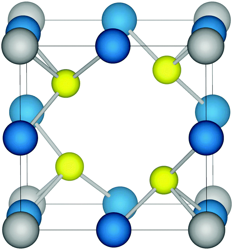 | ||
| Fig. 1 The structure of the cubic chalcogenides Cu3MCh4 (M = V, Nb, Ta; Ch = S, Se, Te). Copper ions, transition metal ions, and chalcogen anions are shown in blue, grey, and yellow, respectively. | ||
Optical absorption measurements by Newhouse et al.40 found the optical band gaps of Cu3TaS4 and Cu3TaSe4 to be 2.70 eV and 2.35 eV, respectively, with visible photoluminescence of Cu3TaS4 upon the absorption of UV light also reported.41 Van Arkel and Crevecoeur42 prepared the compounds Cu3VS4, Cu3NbS4, Cu3TaS4, Cu3VSe4, Cu3NbSe4, and Cu3TaSe4 and reported both V systems to be black, a characteristic indicative of compounds with small band gaps. Cu3NbS4, Cu3TaS4, Cu3NbSe4, and Cu3TaSe4 were found to be green, yellow, red, and green, respectively, suggesting that they have larger band gaps than the corresponding V systems although smaller than the limit for optical transparency. Petritis et al. reported a band gap of 1.3 eV measured by infrared absorption for Cu3VS4 and also determined Cu3TaS4 to be yellow-green in line with the previous study, although the colour of Cu3NbS4 was found in this instance to be red instead of green.43 Thin film Cu3VS4 prepared by pulsed laser deposition (PLD) is also reported to be black with a band gap of 1.35 eV determined by spectroscopic ellipsometry.44
Two previous density functional theory (DFT) studies performed with the PBE functional45 reported fundamental indirect band gaps for Cu3VS4, Cu3NbS4, and Cu3TaS4 of 1.02 eV, 1.64 eV, and 1.91 eV, respectively,46 and 1.041 eV, 1.667 eV, and 1.815 eV, respectively,47 although underestimation of band gap magnitude is a well documented issue with PBE calculations.48,49 An investigation with Bader analysis predicted effective charges of 0.5, 1.5, and −0.75 on the Cu, transition metal, and S ions, respectively.50 Calculations using the full-potential augmented plane wave plus local orbitals (FP-APW+lo) method also reported fundamental indirect band gaps between the R and X k-points for Cu3VSe4, Cu3NbSe4, and Cu3TaSe4.51
In this study, we show how varying the elements in isostructural ternary compounds can change the geometric and electronic structure of a material and therefore be used to tune properties relevant to particular applications. By close examination of the Cu-based chalcogenide series Cu3MCh4 (M = V, Nb, Ta; Ch = S, Se, Te), we outline how the electronic structure of each system is influenced by its constituent elements and compare the nine systems by means of a band gap alignment. From this, we suggest a variety of potential applications based on the wide range of band gaps obtained and propose that alloying materials within such a family could allow for precise control of properties such as band gap.
2 Methods
All calculations were performed with the Vienna ab initio simulation package (VASP),52,53 which utilises the projector augmented wave (PAW) method54,55 to describe interactions between the core (Cu:[Mg], V:[Mg], Nb:[Ca], Ta:[Sr], S:[Ne], Se:[Ar], Te:[Kr]) and valence electrons. A plane wave cut-off of 400 eV and a k-point mesh of Γ-centred 4 × 4 × 4 were employed, and calculations were deemed to be converged when residual forces on each atom were less than 0.01 eV Å−1.One of the inherent flaws in DFT is the self-interaction error (SIE), in which inexact cancellation of the self Coulomb interaction and the exchange functional results in the effective interaction of an electron with itself. To combat this, the empirical +U correction of Dudarev et al.56 is used in conjunction with the PBEsol functional, which was specifically developed to model the properties of solids.57 The validity of the +U method to provide improved structural and electronic descriptions of systems with partially occupied orbitals has been widely demonstrated for a range of solid state materials, including both n-58–61 and p-type semiconductors.62–65 A U of 5.2 eV was applied to the Cu d states, a value which has been shown to reproduce the VB features of a range of CuI-based materials.66–68 This value was originally selected to model the electronic structure of Cu2O with PBE+U in comparison to X-ray photoelectron spectroscopy (XPS),68–70 so to verify the suitability of the same U for PBEsol, Cu2O calculated with PBEsol+U and U = 5.2 eV was also compared to XPS.
Structural optimization was performed over a range of constrained volumes, and the equilibrium cell volume was found by fitting the energy–volume curve to the Murnaghan equation of state,71 which minimizes the associated problem of Pulay stress.72 Electronic density of states (EDOS) and band structure calculations were then performed for each of the chalcogenide systems. To determine the optical properties of the systems, the optical transition matrix elements and the optical absorption spectrum were calculated using the transversal approximation method, which sums the absorption spectra over direct VB to CB transitions.73 The high symmetry points used to generate band structures in this paper are taken from the handbook of Bradley and Cracknell,74 with a schematic of the Brillouin Zone available online on the Bilbao Crystallographic Server.75
To determine the relative energy of the VBs in the systems, an important consideration when combining materials in alloys or heterojunctions, VB offsets were calculated using a procedure analogous to that developed by Wei and Zunger.76,77 To align the valence band maximum (VBM) of each of the systems, the difference between the VBM and Cu 1s core levels (CL) were obtained in each of the separate materials. The compounds were ordered by increasing lattice parameter, and for each consecutive pair of systems, a 48 atom 1 × 1 × 6 supercell was created at the average lattice constant of the two, consisting of three unit cells from each of the two original systems. The supercells were relaxed so that resultant forces were less than 0.01 eV Å−1 and the energy difference of the two CL in the heterostructure was calculated. The VBM offset between each pair of systems was found by aligning the CL of each separate material with the CL offset obtained from the supercell. To determine the relative position of the conduction band minimum (CBM) for each compound, the calculated fundamental band gaps are added to the VBM energies.
3 Results
The calculated lattice parameters of the nine systems are shown in Table 1, with the results listed alongside previously reported experimental values for comparison. Good agreement with experiment is achieved, with underestimation by less than 1% observed in all cases. As experimental lattice constants are usually obtained at room temperature, it is expected that the computationally determined athermal values reported here are slightly smaller. The cell volumes increase down both the transition metal and chalcogenide series due to the increasing atomic radii. For each chalcogen, there is less than a 0.01 Å difference in the lattice constants of the Nb and Ta systems, significantly less than the difference between analogous V and Nb systems, suggesting that the Nb and Ta compounds might be alloyed with minimal strain. This is consistent with previous reports of the ionic radii of Nb and Ta, which are the same in several coordination environments.78| PBEsol+U | Experimental | |
|---|---|---|
| Cu3VS4 | 5.358 | 5.39,42 5.391,43 5.393(1)79 |
| Cu3NbS4 | 5.472 | 5.50,42 5.500,43 5.5001(6)80 |
| Cu3TaS4 | 5.480 | 5.52,42 5.5185,81 5.5145(1)82 |
| Cu3VSe4 | 5.557 | 5.57,42 5.5636(5)83 |
| Cu3NbSe4 | 5.641 | 5.65,42 5.638(1)84 |
| Cu3TaSe4 | 5.650 | 5.67,42 5.6625,81 5.6600(1)38 |
| Cu3VTe4 | 5.838 | — |
| Cu3NbTe4 | 5.902 | 5.9217(1)85 |
| Cu3TaTe4 | 5.906 | 5.9283,81 5.930(2)86 |
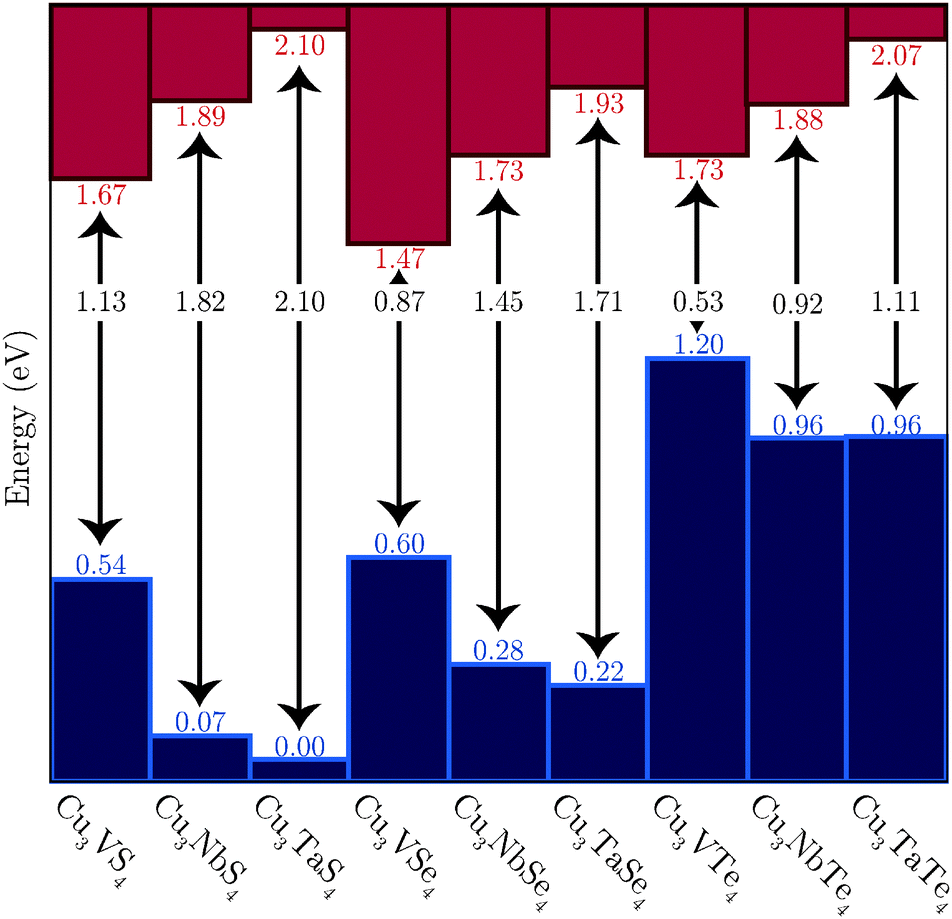
The band structures of all nine systems are shown in Fig. 2, with the calculated direct and indirect band gaps presented in Table 2. Both the VB and CB contain reasonably dispersed bands, although the greatest curvature in the CB does not actually occur in the lowest energy unoccupied bands, which are less dispersed and more densely grouped than those higher in energy. The band structures reveal that all of the systems are predicted to possess indirect fundamental band gaps, with the VBM and CBM at the R and X points, respectively. The direct band gap is at the M point for the three V systems and at the X point for the Nb and Ta materials. Cu3VTe4 has the smallest band gap, with a direct band gap of 0.93 eV and an indirect band gap of 0.53 eV. Cu3TaS4 is determined to have the largest band gap of the series, with a direct band gap of 2.60 eV and an indirect band gap of 2.10 eV. The band gaps are seen to decrease down the Ch group and increase down the M group.
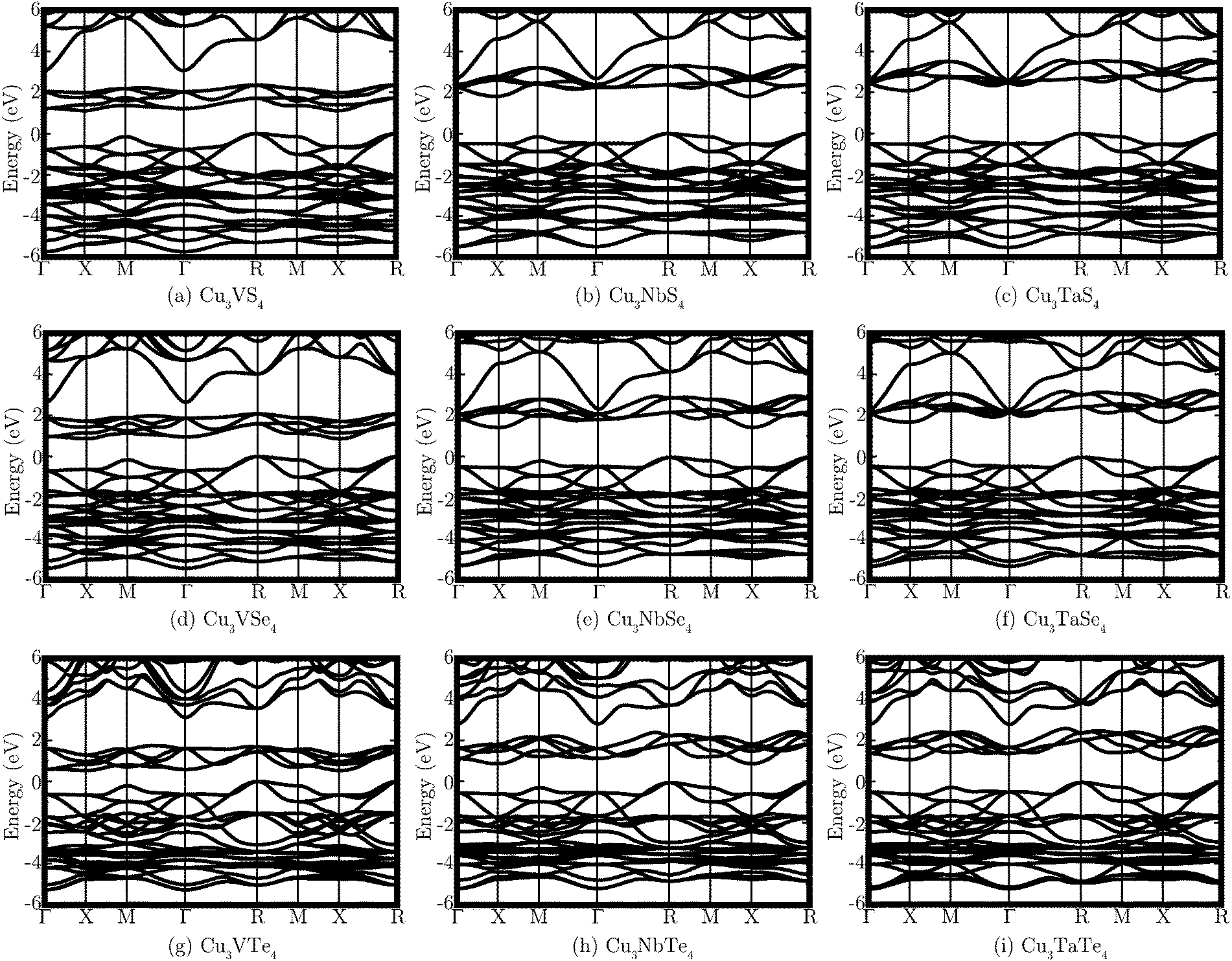 | ||
| Fig. 2 PBEsol+U band structures of each of the nine systems Cu3MCh4 (M = V, Nb, Ta; Ch = S, Se, Te), with the VBM set to 0 eV in all cases. | ||
| E dg | E ig | E optg | E g(expt.) | |
|---|---|---|---|---|
| Cu3VS4 | 1.51 (M) | 1.13 (R → X) | 1.72 (R) | 1.3,43 1.3544 |
| Cu3NbS4 | 2.31 (X) | 1.82 (R → X) | 2.31 (X) | — |
| Cu3TaS4 | 2.60 (X) | 2.10 (R → X) | 2.60 (X) | 2.7040 |
| Cu3VSe4 | 1.28 (M) | 0.87 (R → X) | 1.49 (X) | — |
| Cu3NbSe4 | 1.95 (X) | 1.45 (R → X) | 1.95 (X) | — |
| Cu3TaSe4 | 2.22 (X) | 1.71 (R → X) | 2.22 (X) | 2.3540 |
| Cu3VTe4 | 0.93 (M) | 0.53 (R → X) | 1.19 (X) | — |
| Cu3NbTe4 | 1.46 (X) | 0.92 (R → X) | 1.46 (X) | — |
| Cu3TaTe4 | 1.69 (X) | 1.11 (R → X) | 1.69 (X) | — |
The calculated optical band gaps are also shown in Table 2, with the Nb and Ta systems shown to have an optical band gap the same as the direct band gap at X. However, while this transition is dipole allowed, the absorption is weak between the band edges and strong absorption at this k-point is not predicted until transitions 0.6–0.8 eV higher in energy occur. For the V materials, the lowest energy direct transition at M is optically forbidden, and the optical band gap is instead at X for Cu3VSe4 and Cu3VTe4 and at R for Cu3VS4. The difference in the optical gap between R and X in Cu3VS4 is small, with values of 1.72 eV and 1.76 eV, respectively. While transitions between the band edges at M are forbidden and those at X are weak, optical band gaps at both R and Γ show far stronger absorption and are between 0.02 eV and 0.43 eV higher in energy.
The charge density of the top of the VB and the bottom of the CB at M, X, and Γ, which show forbidden, weak, and strong optical transitions, respectively, was calculated, with the charge density of Cu3VTe4 presented as an example in Fig. 3. The highest occupied band at M is primarily contributed to by Te p states, while the lowest unoccupied band at the same k-point consists only of V d density, resulting in negligible overlap between the two states. At X, while the top of the VB is still dominated by Te p states with some Cu d density, both metals contribute d state density to both the highest occupied band and the lowest unoccupied band, resulting in an optically allowed, albeit weak, d–d transition. However, at Γ, while there is some contribution from Cu d, M d density dominates both the occupied and unoccupied states, leading to significant overlap between the states and a strong transition.
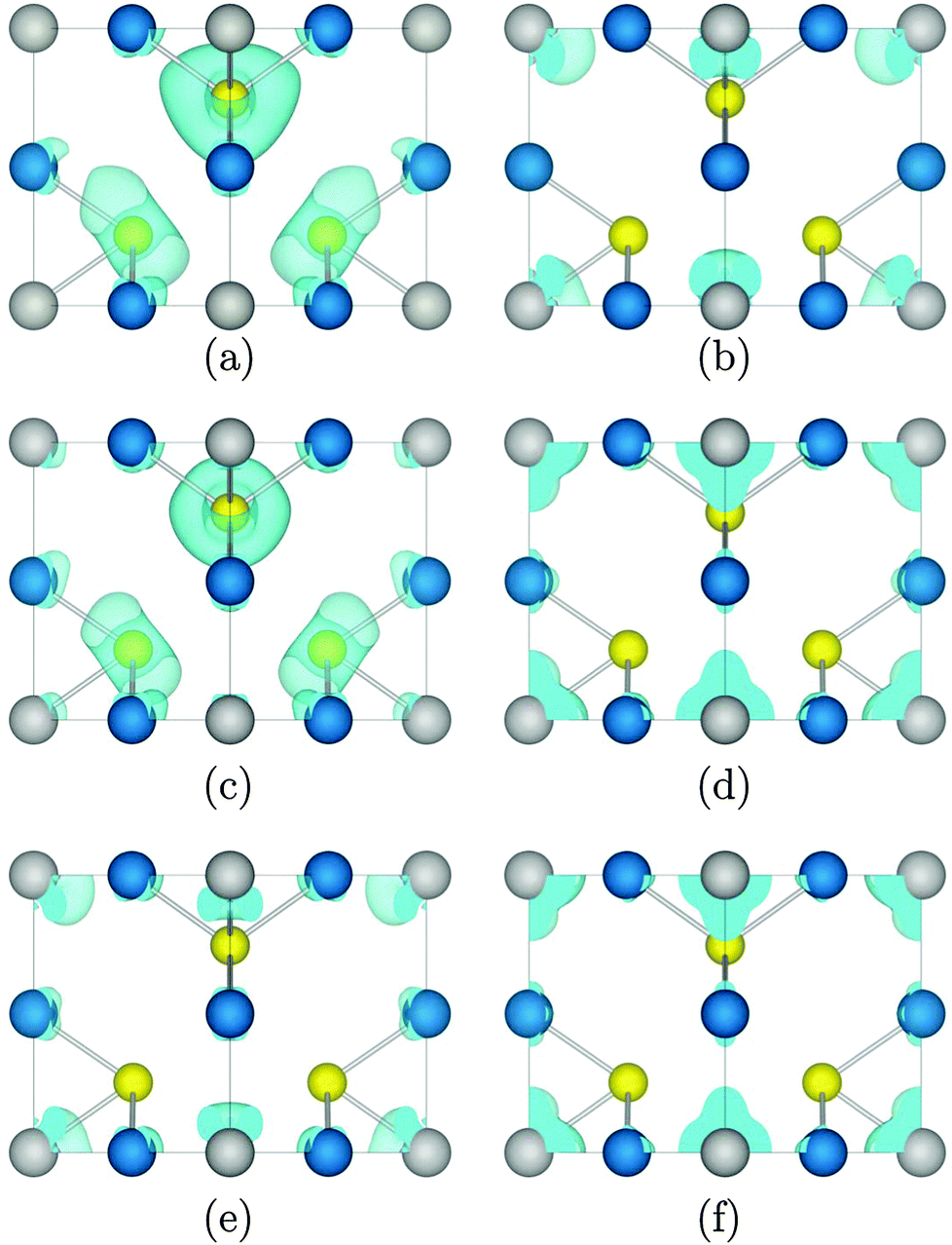 | ||
| Fig. 3 The calculated charge density of (a) the highest occupied band at M, (b) the lowest unoccupied band at M, (c) the highest occupied band at X, (d) the lowest unoccupied band at X, (e) the highest occupied band at Γ, and (f) the lowest unoccupied band at Γ in Cu3VTe4. The isosurface is set to 0.03 eV Å−3. Cu, M, and Ch ions are shown in blue, grey, and yellow, respectively. | ||
The PBEsol+U optical band gaps provide good agreement with experiment, although it should be noted that there are a limited number of studies on these materials in the literature so only a few values are available for comparison. For Cu3TaS4 and Cu3TaSe4, the systems with the largest optical band gaps of 2.60 eV and 2.22 eV, respectively, good agreement is obtained with experimental band gaps measured by optical absorption of 2.70 eV and 2.35 eV.40 However, these are too small for optical transparency, ruling out these systems for TCM applications. The calculated optical band gap of Cu3VS4, at 1.72 eV, agrees less well with experimental reports of 1.3 eV43 and 1.35 eV,44 although the former was estimated via infrared absorption and showed significant temperature dependence while the latter was determined by spectroscopic ellipsometry, which does not yield the band gap directly but fits the dielectric function to a chosen model. In addition, the calculated band gaps of Cu3VS4 and Cu3VSe4 correspond to wavelengths of greater than 700 nm, concurring with reports that these materials are black in colour.42 Similarly, the small band gap of Cu3NbSe4 is predicted to absorb photons of 636 nm and below such that only red light is reflected, in agreement with this compound's observed colour, and Cu3NbS4, Cu3TaS4, and Cu3TaSe4 have the largest optical band gaps of the series, which result in green, yellow, and green materials.42
The calculated carrier effective masses at both the VBM and CBM are shown in Table 3. The lightest hole effective mass is in the R to Γ direction, with the values decreasing down the chalcogen group and in most cases increasing down the transition metal group. The three Te materials have the lightest hole effective masses of the series and are therefore the most likely to display good p-type mobility, with Cu3VTe4 having the lowest value of 0.607mh*. For the electron effective mass at the CBM, similar values are observed in both the M and R directions. Cu3TaTe4 is the material with the lightest electron effective mass, with a value of 0.693me* along the line to R. In comparison, the hole effective mass of p-type semiconductor Cu2O has been experimentally determined to be 0.58mh*,87 while the electron effective mass of n-type In2O3 has been reported both computationally and experimentally as 0.30me*.88,89
| Valence band (m*) | Conduction band (m*) | ||||||
|---|---|---|---|---|---|---|---|
| R → Γ | S | Se | Te | X → Γ | S | Se | Te |
| V | 0.865 | 0.766 | 0.607 | V | 3.005 | 3.066 | 3.125 |
| Nb | 0.951 | 0.830 | 0.640 | Nb | 2.232 | 2.569 | 2.249 |
| Ta | 0.944 | 0.831 | 0.648 | Ta | 3.394 | 3.960 | 3.102 |
| R → M | S | Se | Te | X → M | S | Se | Te |
| V | 3.709 | 3.110 | 1.942 | V | 1.312 | 1.156 | 1.242 |
| Nb | 3.452 | 2.645 | 1.553 | Nb | 0.925 | 0.790 | 0.744 |
| Ta | 3.546 | 2.888 | 1.642 | Ta | 0.883 | 0.744 | 0.700 |
| R → X | S | Se | Te | X → R | S | Se | Te |
| V | 1.074 | 0.942 | 0.738 | V | 1.324 | 1.181 | 1.227 |
| Nb | 1.164 | 0.987 | 0.750 | Nb | 0.935 | 0.797 | 0.736 |
| Ta | 1.154 | 1.008 | 0.764 | Ta | 0.891 | 0.738 | 0.693 |
The calculated EDOS for each of the nine compounds are shown in Fig. 4. The VBM are aligned to 0 eV, but due to the smearing employed in plotting the EDOS, the small band gap of Cu3VTe4 is difficult to visually distinguish. The VB displays significant density of Cu 3d, M nd (M = V, n = 3; M = Nb, n = 4; M = Ta, n = 5), and Ch mp (Ch = S, m = 3; Ch = Se, m = 4; Ch = Te, m = 5) states. The CB is primarily composed of M nd states, with smaller contributions from the Cu 3d and Ch mp states. There is significantly less Cu 3d density near the top of the VB in the Te systems compared to the S and Se systems, and the main Cu d peak is shifted lower in energy down the chalcogen group. For the V compounds, the V 3d states dominate the bottom of the CB, but for the Nb and Ta systems, more mixing with the Cu d and Ch mp states is observed. It should be noted that only the Cu d, M d, and Ch p states are shown in the EDOS as they account for almost all contribution to the band edges. However, the peak beginning at approximately 4 eV, which corresponds to the most dispersed bands in the band structure, also comprises density from Cu s and p states, M s and p states, and Ch s and d states (excluding d states for sulphur).
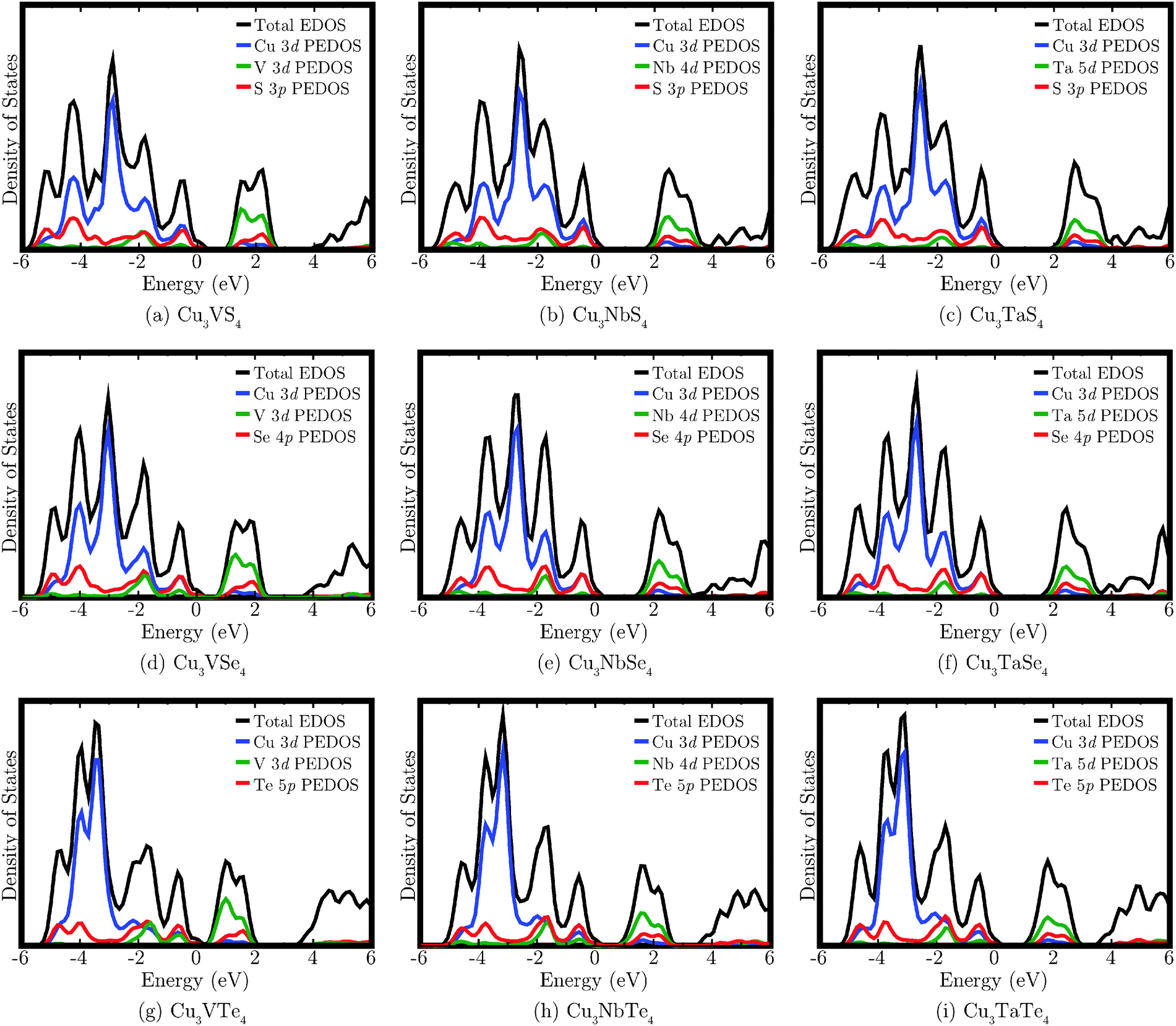 | ||
| Fig. 4 The calculated density of states for Cu3MCh4 (M = V, Nb, Ta; Ch = S, Se, Te). In each case, the VBM has been aligned to 0 eV and a 0.2 eV Gaussian broadening has been applied to each EDOS. | ||
The PBEsol+U calculated VB offsets are shown in Fig. 5, with the VBM energies shown relative to that of the lowest VB, that of Cu3TaS4, and the positions of the CBM based on the calculated band gaps. Two competing trends are in evidence. Firstly, the VBM decreases in energy and the CBM increases in energy down the M (M = V, Nb, Ta) series, leading to progressively wider band gaps. Secondly, the band gap decreases down the Ch (Ch = S, Se, Te) group, with the VB being raised and the CB simultaneously lowered.
 | ||
| Fig. 5 The offset of the VBM of the nine systems, as determined with PBEsol+U. The corresponding CBM are based on the indirect band gaps calculated with PBEsol+U. | ||
Bader charge analysis calculations were performed on the optimised charge densities of the systems, with the findings summarised in Table 4. The formal charges of the species involved are +1 for the Cu, +5 for the transition metal, and −2 for the chalcogen. It was found that there are effective charges of between 0.03 and 0.37 on the Cu ions, between 1.05 and 1.66 on M (M = V, Nb, Ta) ions, and between −0.31 and −0.67 on Ch (Ch = S, Se, Te) ions. The overall covalency is seen to increase down the Ch group as the electronegativity of the chalcogen ions decreases, although there is a competing trend whereby the Bader charges on the M and Ch ions increase down the M group. The least covalent compound is therefore Cu3TaS4 and the most covalent is Cu3VTe4, which correspond to the systems with the largest and smallest band gaps of the family, respectively.
| Cu | M | Ch | |||||||
|---|---|---|---|---|---|---|---|---|---|
| S | Se | Te | S | Se | Te | S | Se | Te | |
| V | 0.37 | 0.24 | 0.03 | 1.38 | 1.21 | 1.05 | −0.62 | −0.48 | −0.29 |
| Nb | 0.35 | 0.23 | 0.04 | 1.54 | 1.36 | 1.12 | −0.65 | −0.51 | −0.31 |
| Ta | 0.34 | 0.22 | 0.04 | 1.66 | 1.47 | 1.20 | −0.67 | −0.54 | −0.33 |
4 Discussion
The band gap energies obtained with PBEsol+U offer good agreement with the limited experimental data available. The band gap magnitudes displayed across the nine systems show two independent trends that result from moving down the M (M = V, Nb, Ta) and Ch (Ch = S, Se, Te) series. It was observed that the band gap decreases down the chalcogenide group, from S to Se to Te, which is to be expected due to increasingly higher energy p states. Conversely, the band gap increases down the transition metal group, in agreement with previous studies on systems containing group 5 ions, such as InMO4 (M = V, Nb, Ta)90 and SrBi2M2O9 (M = Nb, Ta).91 The increase in band gap magnitude down the group can be explained by analysis of the EDOS, which shows that the bottom of the CB is dominated by M d states that have higher energies in the heavier ions, increasing from V to Nb to Ta.Considering the relatively high electronegativity of chalcogens (particularly S and Se) with respect to the transition metals considered, it might be expected that the VB would be made up almost entirely of chalcogen states. However, the introduction of a closed shell cation, in this case the d10 ion Cu(I), results in mixing between the Cu d states and the chalcogen p states, which helps to delocalise hole states and render p-type electronic transport viable, an approach used with Cu-based oxides such as delafossites.3 It is also found that the system with the largest Bader charges on the group five transition metal and the chalcogen, Cu3TaS4, corresponds to the largest band gap; conversely, the most covalent compound, Cu3VTe4, has the smallest band gap. In agreement with the EDOS, more mixing of both the Cu and transition metal ion states with the chalcogen states is observed in the Te systems than in those containing S. Varying the M ion results in increasing the effective charge on M down the transition metal group while decreasing the charge on the Cu and Ch ions.
In all cases, the values of electron and hole effective mass are quite close, suggesting that these systems could act as either p- or n-type semiconductors. The hole effective mass is seen to have a strong dependence on the Ch ion, with the Te systems having the lightest hole effective mass and the S materials having the heaviest. Conversely, the electron effective mass varies most significantly with the M ion, as the V systems possess higher electron effective masses while the Nb and Ta systems have far lighter electron effective masses. As such, Cu3TaTe4 has relatively low carrier effective masses at both the VBM and CBM, with Cu3NbSe4, Cu3NbTe4, and Cu3TaSe4 also showing reasonable values at both band edges.
In the context of current PV technology, the adsorber layer should ideally be p-type, with a high VBM and a low hole effective mass. The system with the highest VBM is Cu3VTe4. Its VB electrons are closest to the vacuum and holes could therefore be created with relative ease, so this material is predicted to be the most susceptible to p-type doping. From the effective mass calculations, the system is also likely to have good p-type mobility. In general, the systems with lower hole effective mass also have higher VBMs, and all three Te materials are therefore potential p-type materials. Cu3VSe4 has the lowest CBM of all the systems and is therefore the most likely to support n-type doping, an interesting result as these two systems differ only in the chalcogen ion but are predicted to have markedly different properties. However, the electron effective mass of Cu3VSe4 is relatively high compared to the Nb and Ta systems.
Cu3VTe4, Cu3NbTe4, Cu3VSe4, Cu3TaTe4, and Cu3VS4 have optical band gaps potentially suited to photovoltaic application, with values of 1.19 eV, 1.46 eV, 1.49 eV, 1.69 eV, and 1.72 eV, respectively. All of these systems are predicted to show reasonable p-type conductivity, particularly the three Te systems, which is the usual polarity of PV absorber materials. In addition, the antibonding states at the top of the VB are indicative of defect tolerant systems, i.e. ones in which the presence of defects do not affect the optoelectronic properties of the compound and where defect states are typically shallow, which is necessary for high conductivity.92 The band gaps of all nine systems are below the threshold for optical transparency of 3 eV, with the largest optical band gap that of Cu3TaS4 at 2.60 eV, effectively ruling these materials out as TCMs.
The energy difference between the VBM of the Nb and Ta systems is in all cases small (<0.1 eV), as is the difference is their lattice constants (<0.01 Å), a point of interest when considering the compatibility of materials upon alloying. For example, Cu3NbTe4 and Cu3TaTe4 have very similar lattice constants of 5.641 Å and 5.650 Å, respectively, differ in their VBM energies by just 0.06 eV, and have respective optical band gaps of 1.46 eV and 1.69 eV. By combining the two materials and varying the concentrations of Nb and Ta ions in the mixed system, the band gap could theoretically be tuned to any value between 1.46 eV and 1.69 eV.
5 Conclusion
The electronic structure of nine sulvanite structured semiconductors Cu3MCh4 (M = V, Nb, Ta; Ch = S, Se, Te) has been elucidated with PBEsol+U in order to rationalise trends in the optoelectronic properties of the series and to identify potential candidates for optoelectronic applications. Five materials were identified as having optical band gaps in the appropriate range for PV absorbers, namely Cu3VTe4, Cu3NbTe4, Cu3VSe4, Cu3TaTe4, and Cu3VS4, with band gap values of 1.19 eV, 1.46 eV, 1.49 eV, 1.69 eV, and 1.72 eV, respectively. Cu3VTe4 also has the highest VBM in the series, making it the most likely to exhibit p-type behaviour, and is predicted to have the highest p-type mobility of the nine materials, all of which is indicative of a potential PV absorber. None of the systems were found to have band gaps of large enough magnitude to result in optical transparency, so potential TCM application of any of these materials is therefore unlikely. The VB alignment shows that each pair of Nb and Ta compounds have VBMs close in energy as well as similar lattice constants, which increases their potential to be successfully alloyed for the purpose of tuning properties such as band gap. The range of calculated band gaps over the series evidences how varying the composition of ternary compounds can strongly influence the electronic structure. In addition, it poses the question as to how alloying isostructural materials with different band gap magnitudes can be exploited to tune electronic properties to specific optoelectric applications.Acknowledgements
This research was supported by SFI (grant numbers 09/RFP/MTR2274 and 12/IA/1414). Calculations were performed on HECToR and ARCHER via membership of the Materials Chemistry Consortium (funded by EPSRC grant number EP/L000202), the DJEI/DES/SFI/HEA Irish Centre for High-End Computing (ICHEC) platform Fionn, and the Lonsdale cluster maintained by TCHPC. A. B. K. is grateful to the Irish Research Council EMBARK initiative for the provision of a postgraduate scholarship.References
- F. Odobel, L. Le Pleux, Y. Pellegrin and E. Blart, Acc. Chem. Res., 2010, 43, 1063–1071 CrossRef CAS PubMed.
- M. G. Walter, E. L. Warren, J. R. McKone, S. W. Boettcher, Q. X. Mi, E. A. Santori and N. S. Lewis, Chem. Rev., 2010, 110, 6446–6473 CrossRef CAS.
- H. Kawazoe, H. Yasakuwa, H. Hyodo, M. Kurita, H. Yanagi and H. Hosono, Nature, 1997, 389, 939–942 CrossRef CAS.
- K. L. Chopra, P. D. Paulson and V. Dutta, Prog. Photovoltaics, 2004, 12, 69–92 CAS.
- R. W. Miles, G. Zoppi and I. Forbes, Mater. Today, 2007, 10, 20–27 CrossRef CAS.
- S. Y. Chen, A. Walsh, J. H. Yang, X. G. Gong, L. Sun, P. X. Yang, J. H. Chu and S. H. Wei, Phys. Rev. B: Condens. Matter Mater. Phys., 2011, 83, 125201 CrossRef.
- H. Katagiri, Thin Solid Films, 2005, 480, 426–432 CrossRef.
- M. A. Green, K. Emery, Y. Hishikawa, W. Warta and E. D. Dunlop, Prog. Photovoltaics, 2014, 22, 701–710 Search PubMed.
- N. Feldberg, J. D. Aldous, W. M. Linhart, L. J. Phillips, K. Durose, P. A. Stampe, R. J. Kennedy, D. O. Scanlon, G. Vardar, R. L. Field, III, T. Y. Jen, R. S. Goldman, T. D. Veal and S. M. Durbin, Appl. Phys. Lett., 2013, 103, 042109 CrossRef.
- L. Lahourcade, N. C. Coronel, K. T. Delaney, S. K. Shukla, N. A. Spaldin and H. A. Atwater, Adv. Mater., 2013, 25, 2562–2566 CrossRef CAS PubMed.
- D. O. Scanlon and A. Walsh, Appl. Phys. Lett., 2012, 100, 251911 CrossRef.
- J. Burschka, N. Pellet, S.-J. Moon, R. Humphry-Baker, P. Gao, M. K. Nazeeruddin and M. Gratzel, Nature, 2013, 499, 316–319 CrossRef CAS PubMed.
- M. Liu, M. B. Johnston and H. J. Snaith, Nature, 2013, 501, 395–398 CrossRef CAS PubMed.
- D. S. Bhachu, D. O. Scanlon, E. J. Saban, H. Bronstein, I. P. Parkin, C. J. Carmalt and R. G. Palgrave, J. Mater. Chem. A, 2015, 3, 9071–9073 CAS.
- A. Walsh, D. O. Scanlon, S. Chen, X. G. Gong and S.-H. Wei, Angew. Chem., Int. Ed., 2015, 54, 1791–1794 CrossRef CAS PubMed.
- M. D. McGehee, Nature, 2013, 501, 323–325 CrossRef CAS PubMed.
- T. Minami, MRS Bull., 2000, 25, 38–44 CrossRef CAS.
- R. G. Gordon, MRS Bull., 2000, 25, 52–57 CrossRef CAS.
- D. O. Scanlon, A. Walsh and G. W. Watson, Chem. Mater., 2009, 21, 4568–4576 CrossRef CAS.
- K. G. Godinho, B. J. Morgan, J. P. Allen, D. O. Scanlon and G. W. Watson, J. Phys.: Condens. Matter, 2011, 23, 334201 CrossRef CAS PubMed.
- D. O. Scanlon, K. G. Godinho, B. J. Morgan and G. W. Watson, J. Chem. Phys., 2010, 132, 024707 CrossRef PubMed.
- D. Shin, J. S. Foord, D. J. Payne, T. Arnold, D. J. Aston, R. G. Egdell, K. G. Godinho, D. O. Scanlon, B. J. Morgan, G. W. Watson, E. Mugnier, C. Yaicle, A. Rougier, L. Colakerol, P. A. Glans, L. F. J. Piper and K. E. Smith, Phys. Rev. B: Condens. Matter Mater. Phys., 2009, 80, 233105 CrossRef.
- H. Kawazoe and K. Ueda, J. Am. Ceram. Soc., 1999, 82, 3330–3336 CrossRef CAS.
- M. Dekkers, G. Rijnders and D. H. A. Blank, Appl. Phys. Lett., 2007, 90, 021903 CrossRef.
- S. Inoue, K. Ueda, H. Hosono and N. Hamada, Phys. Rev. B: Condens. Matter Mater. Phys., 2001, 64, 245211 CrossRef.
- K. Ueda, S. Inoue, S. Hirose, H. Kawazoe and H. Hosono, Appl. Phys. Lett., 2000, 77, 2701–2703 CrossRef CAS.
- K. Ueda, H. Hosono and N. Hamada, J. Phys.: Condens. Matter, 2004, 16, 5179–5186 CrossRef CAS.
- N. Duan, A. W. Sleight, M. K. Jayaraj and J. Tate, Appl. Phys. Lett., 2000, 77, 1325–1326 CrossRef CAS.
- H. Yanagi, S. Inoue, K. Ueda, H. Kawazoe, H. Hosono and N. Hamada, J. Appl. Phys., 2000, 88, 4059–4163 CrossRef.
- H. Hiramatsu, K. Ueda, H. Ohta, M. Orita, M. Hirano and H. Hosono, Appl. Phys. Lett., 2002, 81, 598–600 CrossRef CAS.
- C. R. A. Catlow, Z. X. Guo, M. Miskufova, S. A. Shevlin, A. G. H. Smith, A. A. Sokol, A. Walsh, D. J. Wilson and S. M. Woodley, Philos. Trans. R. Soc., A, 2010, 368, 3379–3456 CrossRef CAS PubMed.
- A. Walsh, Y. Yan, M. N. Huda, M. M. Al-Jassim and S. H. Wei, Chem. Mater., 2009, 21, 547–551 CrossRef CAS.
- R. Nitsche and P. Wild, J. Appl. Phys., 1967, 38, 5413–5414 CrossRef CAS.
- S. Sheng, G. Fang, C. Li, S. Xu and X. Zhao, Phys. Status Solidi, 2006, 203, 1891–1900 CrossRef CAS.
- D. J. Temple, A. B. Kehoe, J. P. Allen, G. W. Watson and D. O. Scanlon, J. Phys. Chem. C, 2012, 116, 7334–7340 CAS.
- A. B. Kehoe, D. J. Temple, G. W. Watson and D. O. Scanlon, Phys. Chem. Chem. Phys., 2013, 15, 15477–15484 RSC.
- U.S. Geological Survey, Mineral Commodity Summaries 2015, United States Government Printing Office, Washington, D.C., 2015 Search PubMed.
- G. E. Delgado, A. J. Mora, S. Duran, M. Munoz and P. Grima-Gallardo, J. Alloys Compd., 2007, 439, 346–349 CrossRef CAS.
- H. Arribart, B. Sapoval, O. Gorochov and N. Lenavard, Solid State Commun., 1978, 26, 435–439 CrossRef CAS.
- P. F. Newhouse, P. A. Hersh, A. Zakutayev, A. Richard, H. A. S. Platt, D. A. Keszler and J. Tate, Thin Solid Films, 2009, 517, 2473–2476 CrossRef CAS.
- J. Tate, P. F. Newhouse, R. Kykyneshi, P. A. Hersh, J. Kinney, D. H. McIntyre and D. A. Keszler, Thin Solid Films, 2008, 516, 5795–5799 CrossRef CAS.
- A. E. Van Arkel and C. Crevecoeur, J. Less-Common Met., 1963, 5, 177–180 CrossRef.
- D. Petritis, G. Martinez, C. Levyclement and O. Gorochov, Phys. Rev. B: Condens. Matter Mater. Phys., 1981, 23, 6773–6786 CrossRef CAS.
- X. Lv, Z. Deng, F. Miao, G. Gu, Y. Sun, Q. Zhang and S. Wan, Opt. Mater., 2012, 34, 1451–1454 CrossRef CAS.
- J. P. Perdew, K. Burke and M. Ernzerhof, Phys. Rev. Lett., 1996, 77, 3865–3868 CrossRef CAS PubMed.
- W. Espinosa García, A. Morales Aramburo and J. Osorio Guillén, Revista Colombiana de Física, 2008, 40, 36–39 Search PubMed.
- M. A. Ali, N. Jahan and A. K. M. A. Islam, J. Sci. Res., 2014, 6, 407–419 CAS.
- D. O. Scanlon, A. B. Kehoe, G. W. Watson, M. O. Jones, W. I. F. David, D. J. Payne, R. G. Egdell, P. P. Edwards and A. Walsh, Phys. Rev. Lett., 2011, 107, 246402 CrossRef PubMed.
- A. B. Kehoe, D. O. Scanlon and G. W. Watson, Phys. Rev. B: Condens. Matter Mater. Phys., 2011, 83, 233202 CrossRef.
- J. M. Osorio-Guillen and W. F. Espinosa-Garcia, Phys. B, 2012, 407, 985–991 CrossRef CAS.
- K. Bougherara, F. Litimein, R. Khenata, E. Ugun, H. Y. Ocak, S. Ugur, G. Ugur, A. H. Reshak, F. Soyalp and S. B. Omran, Sci. Adv. Mater., 2013, 5, 97–106 CrossRef CAS.
- G. Kresse and J. Hafner, Phys. Rev. B: Condens. Matter Mater. Phys., 1994, 49, 14251–14271 CrossRef CAS.
- G. Kresse and J. Furthmuller, Comput. Mater. Sci., 1996, 6, 15–50 CrossRef CAS.
- P. E. Blochl, Phys. Rev. B: Condens. Matter Mater. Phys., 1994, 50, 17953–17979 CrossRef.
- G. Kresse and D. Joubert, Phys. Rev. B: Condens. Matter Mater. Phys., 1999, 59, 1758–1775 CrossRef CAS.
- S. L. Dudarev, G. A. Botton, S. Y. Savrasov, C. J. Humphreys and A. P. Sutton, Phys. Rev. B: Condens. Matter Mater. Phys., 1998, 57, 1505–1509 CrossRef CAS.
- J. P. Perdew, A. Ruzsinszky, G. I. Csonka, O. A. Vydrov, G. E. Scuseria, L. A. Constantin, X. Zhou and K. Burke, Phys. Rev. Lett., 2008, 100, 136406 CrossRef PubMed.
- B. J. Morgan and G. W. Watson, Phys. Rev. B: Condens. Matter Mater. Phys., 2010, 82, 144119 CrossRef.
- R. Coquet and D. J. Willock, Phys. Chem. Chem. Phys., 2005, 7, 3819–3828 RSC.
- A. Walsh, Y. Yan, M. M. Al-Jassim and S. H. Wei, J. Phys. Chem. C, 2008, 125, 12044–12050 Search PubMed.
- B. J. Morgan, D. O. Scanlon and G. W. Watson, J. Mater. Chem., 2009, 19, 5175–5178 RSC.
- M. Nolan and G. W. Watson, J. Chem. Phys., 2006, 125, 144701 CrossRef PubMed.
- D. O. Scanlon, A. Walsh, B. J. Morgan, M. Nolan, J. Fearon and G. W. Watson, J. Phys. Chem. C, 2007, 111, 7971–7979 CAS.
- A. B. Kehoe, D. O. Scanlon and G. W. Watson, Chem. Mater., 2011, 23, 4464–4468 CrossRef CAS.
- P. R. Keating, D. O. Scanlon and G. W. Watson, Chem. Phys. Lett., 2014, 608, 239–243 CrossRef CAS.
- D. O. Scanlon, A. Walsh, B. J. Morgan, D. Payne, R. G. Egdell and G. W. Watson, Phys. Rev. B: Condens. Matter Mater. Phys., 2009, 79, 035101 CrossRef.
- T. Arnold, D. J. Payne, A. Bourlange, J. P. Hu, R. G. Egdell, L. F. J. Piper, L. Colakerol, A. De Masi, P. A. Glans, T. Learmonth, K. E. Smith, J. Guo, D. O. Scanlon, A. Walsh, B. J. Morgan and G. W. Watson, Phys. Rev. B: Condens. Matter Mater. Phys., 2009, 79, 075102 CrossRef.
- D. O. Scanlon, B. J. Morgan and G. W. Watson, J. Chem. Phys., 2009, 131, 124703 CrossRef PubMed.
- J. P. Hu, D. J. Payne, R. G. Egdell, P. A. Glans, T. Learmonth, K. E. Smith, J. Guo and N. M. Harrison, Phys. Rev. B: Condens. Matter Mater. Phys., 2008, 77, 155115 CrossRef.
- J. Ghijsen, L. H. Tjeng, J. van Elp, H. Eskes, J. Westerink, G. A. Sawatzky and M. T. Czyzyk, Phys. Rev. B: Condens. Matter Mater. Phys., 1988, 38, 11322–11330 CrossRef CAS.
- F. D. Murnaghan, Proc. Natl. Acad. Sci. U. S. A., 1944, 30, 244–247 CrossRef CAS.
- J. P. Allen, D. O. Scanlon, S. C. Parker and G. W. Watson, J. Phys. Chem. C, 2011, 115, 19916–19924 CAS.
- M. Gajdos, K. Hummer, G. Kresse, J. Furthmuller and F. Bechstedt, Phys. Rev. B: Condens. Matter Mater. Phys., 2006, 73, 045112 CrossRef.
- C. J. Bradley and A. P. Cracknell, Mathematical Theory of Symmetry in Solids, Oxford Univeristy Press, 1972 Search PubMed.
- M. I. Aroyo, J. M. Perez-Mato, D. Orobengoa, E. Tasci, G. de la Flor and A. Kirov, Bulg. Chem. Commun., 2011, 43, 183–197 CAS.
- S.-H. Wei and A. Zunger, Appl. Phys. Lett., 1998, 72, 2011–2013 CrossRef CAS.
- S.-H. Wei and A. Zunger, Phys. Rev. Lett., 1987, 59, 144–147 CrossRef CAS PubMed.
- R. D. Shannon, Acta Crystallogr., 1976, 32, 751–767 CrossRef.
- C. Mujica, G. Carvajal, J. Llanos and O. Wittke, Z. Kristallogr. – New Cryst. Struct., 1998, 213, 12 CAS.
- M. Kars, A. Rebbah and H. Rebbah, Acta Crystallogr., Sect. E: Struct. Rep. Online, 2005, 61, I180–I181 CAS.
- K. Zitter, J. Schmand, K. Wagner and R. Schöllhorn, Mater. Res. Bull., 1984, 19, 801–805 CrossRef CAS.
- G. E. Delgado, J. E. Contreras, A. J. Mora, S. Durn, M. Muoz and P. Grima-Gallardo, Acta Phys. Pol., A, 2011, 120, 468–472 CAS.
- K. O. Klepp and D. Gurtner, Z. Kristallogr. NCS., 2000, 215, 4 CAS.
- Y. J. Lu and J. A. Ibers, J. Solid State Chem., 1993, 107, 58–62 CrossRef CAS.
- G. E. Delgado, A. J. Mora, P. Grima-Gallardo, S. Duran, M. Munoz and M. Quintero, Chalcogenide Lett., 2009, 6, 335–338 CAS.
- J. Li and H. Y. Guo, J. Solid State Chem., 1995, 117, 247–255 CrossRef CAS.
- J. W. Hodby, T. E. Jenkins, C. Schwab, H. Tamura and D. Trivich, J. Phys. C: Solid State Phys., 1976, 9, 1429–1439 CrossRef CAS.
- N. Preissler, O. Bierwagen, A. T. Ramu and J. S. Speck, Phys. Rev. B: Condens. Matter Mater. Phys., 2013, 88, 085305 CrossRef.
- D. O. Scanlon, A. Regoutz, R. G. Egdell, D. J. Morgan and G. W. Watson, Appl. Phys. Lett., 2013, 103, 262108 CrossRef.
- G.-L. Li and Z. Yin, Phys. Chem. Chem. Phys., 2011, 13, 2824–2833 RSC.
- N. Zhao, Y. H. Wang, X. Y. Zhao, M. Zhang and S. Gong, Chin. Phys. Lett., 2011, 28, 077101 CrossRef.
- A. Zakutayev, C. M. Caskey, A. N. Fioretti, D. S. Ginley, J. Vidal, V. Stevanovic, E. Tea and S. Lany, J. Phys. Chem. Lett., 2014, 5, 1117–1125 CrossRef CAS PubMed.
| This journal is © The Royal Society of Chemistry 2015 |