
 Open Access Article
 This Open Access Article is licensed under a
 Creative Commons Attribution 3.0 Unported Licence
Flexible organic transistors based on a solution-sheared PVDF insulator†
S.
Georgakopoulos
,
F. G.
del Pozo
and
M.
Mas-Torrent
*
Institut de Ciència de Materials de Barcelona (ICMAB-CSIC) and CIBER-BBN, Campus de la UAB, 08193, Bellaterra, Spain. E-mail: mmas@icmab.es
First published on 4th November 2015
Abstract
Organic field-effect transistors are demonstrated in which the insulator–semiconductor stack of the poly(vinylidene fluoride) (PVDF) and polystyrene (PS):dibenzo-tetrathiavulfalene (DB-TTF) blend is deposited by two low-cost and scalable solution shearing steps onto plastic substrates. The PS vertically phase separates upon coating the DB-TTF:PS blend solution and acts as a smoothening and depolarisation layer for the underlying PVDF. The transistors exhibit a mean mobility of 0.2 cm2 V−1 s−1, an on/off ratio of 104 and near-zero threshold voltage with high reproducibility, the same performance as on previously reported Si/SiO2 substrates.
Organic electronics technology utilises materials from solution to enable the production of devices at low cost, on large areas, with high throughput, and onto a variety of substrates including flexible transparent plastics and papers.1 These devices are promising for a large variety of applications such as vapour, pressure and biological sensors,2,3 analog and digital electronic circuits, electrophoretic and even light emitting diode display drivers.4 The fabrication of OFETs on flexible substrates can be challenging due to solvent compatibility issues as well as the high surface roughness of plastics. Often, additional processing steps are required to deposit planarization layers.5 Also, OFETs on plastic substrates can perform inferiorly as compared to those on rigid Si/SiO2 substrates6 since the morphology of the semiconductor thin film can be strongly affected by different underlying surfaces. In order to realise low-cost and mass-produced devices, it is imperative to investigate cheap and easily-processable semiconductors and insulators, the main components of organic field-effect transistors (OFETs), that can be applied on plastic substrates. Those materials must be soluble in orthogonal solvents to prevent damage to the first layer by the deposition of the subsequent layer. Additionally the deposition of the materials should employ solution processing techniques that can be up-scaled. Various examples of semiconductor and insulator printing have been reported utilising techniques such as ink-jet, spray or gravure printing.7
A polymer insulator of interest is poly(vinylidene fluoride) (PVDF). PVDF stores more charge than typical solution processable insulators8 such as Cytop®, poly(vinylphenol) (PVP) and poly(methylmethacrylate) (PMMA) owing to its high permittivity (PVDF εr = 8, Cytop® εr = 2.1, PVP and PMMA εr = 3–4). PVDF is commonly dissolved in highly polar organic solvents (i.e. DMF, DMAc, DMSO) but it is unaffected by other solvents. Thus this polymer is an ideal candidate for bottom-gate applications in which the semiconductor is deposited on top of the insulator and is directly exposed to the environment, which is ideal for vapour and aqueous medium sensing applications that are rapidly gaining momentum in organic electronics.3 In this configuration, spin-coated cross-linked polymers or Cytop® are typically employed, but the current market price of PVDF is significantly lower.
PVDF exhibits multiple morphological phases with paraelectric and ferroelectric properties.9 This material is almost exclusively used in the tetrafluoroethylene copolymer form P(VDF-TrFE), which is more crystalline and exhibits higher ferroelectric response and higher permittivity (P(VDF-TrFE) εr = 10).10 The spin-coated films of P(VDF-TrFE) have been used to demonstrate inorganic9,11 and organic10,12–22 memristors. Many of the aforementioned studies utilise bilayer or trilayer insulator structures to reduce gate leakage where each layer is deposited in a different step (i.e. spin-coating of PVDF followed by spin-coating of PMMA). There is very limited work on the utilisation of paraelectric thin films for OFETs. Jung et al.10 have reported OFETs with no hysteresis based on a P(VDF-TrFE)-PVDF-PMMA blend insulator and F8T2 semiconductor with mobility of 10−4 cm2 V−1 s−1. It is noted that the charge carrier mobility in OFETs has been shown to be inversely proportional to the permittivity of the insulator, as polar insulators contribute to static dipolar disorder.23
We have previously reported24 on the deposition of a blend based on the small molecule semiconductor dibenzo-tetrathiafulvalene (DB-TTF) and the polystyrene insulator (PS) on SiO2, employing a solution meniscus shearing technique that is highly compatible with roll-to-roll production. The deposited films undergo vertical phase separation forming a bottom PS layer and a top DB-TTF layer. This technique has produced thin films of excellent performance and reproducibility with high mobilities (mean 0.2 cm2 V−1 s−1), near-zero threshold voltage (VT), and no hysteresis. This value is very close to the mobility of solution-processed single crystals25 and evaporated polycrystalline films26 of DB-TTF, with which the maxim mobilities of 1 cm2 V−1 s−1 and 0.55 cm2 V−1 s−1, respectively, have been reported. In this work we demonstrate OFETs on flexible poly(ethyleneterephthalate) (PET) substrates (Fig. 1), utilising the PVDF homopolymer to solution-shear paraelectric thin films that exhibit limited hysteresis as compared to reported studies on memristors. The subsequent solution shearing of the semiconducting DB-TTF:PS blend works exceptionally well in combination with PVDF, as the phase separation of the PS layer depolarises (PS εr = 2.4) and smoothens the underlying PVDF layer and the resulting OFETs exhibit the same mobility and reproducibility as on SiO2, without having to coat the PS in a separate step. Importantly, all the fabrication and characterisation steps were performed under ambient conditions and no degradation in the electrical performance of the devices was observed one week after fabrication.
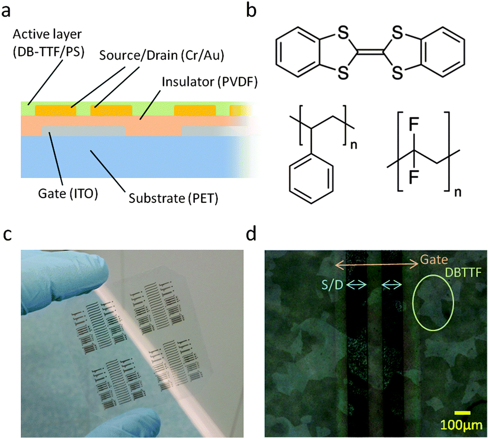 | ||
| Fig. 1 (a) Cross-sectional structure of the sample. (b) Materials used for an active layer and an insulator: DB-TTF, PS, PVDF. (c) Photograph of a finished substrate of 6 cm × 6 cm area. (d) Polarised microscopy image showing the electrodes and large crystalline domains of DB-TTF. | ||
An overview of the fabrication process is given, with a more detailed description in the ESI.† The as-bought PET substrates coated with indium tin oxide (ITO) underwent photolithography and etching processes to pattern gate structures.
PVDF (180![[thin space (1/6-em)]](https://www.rsc.org/images/entities/char_2009.gif) 000 g mol−1) was dissolved in DMF at 10 wt% concentration. The substrate was placed on a coater bed at 120 °C, and a flat blade applicator located 0.88 mm above the substrate sheared the solution forward at a speed of 5 mm s−1. The final layer was 1 μm thick as measured by profilometry. The surface was imaged by atomic force microscopy (AFM), exhibiting circular domains of 5–10 μm diameter and an rms roughness of approximately 53 nm (Fig. 2a). The measured roughness is high and would undoubtedly negatively influence OFET performance without being further smoothened. The measured FTIR spectrum of the PVDF surface (Fig. S1, ESI†) is in good agreement with the reported α-phase9 (also reported as form-II27). The capacitance was measured over frequency for a capacitor of known area (Fig. S2, ESI†) and a relative permittivity of 8 was extracted with a corresponding capacitance per unit area of 7.1 nF cm−2.
000 g mol−1) was dissolved in DMF at 10 wt% concentration. The substrate was placed on a coater bed at 120 °C, and a flat blade applicator located 0.88 mm above the substrate sheared the solution forward at a speed of 5 mm s−1. The final layer was 1 μm thick as measured by profilometry. The surface was imaged by atomic force microscopy (AFM), exhibiting circular domains of 5–10 μm diameter and an rms roughness of approximately 53 nm (Fig. 2a). The measured roughness is high and would undoubtedly negatively influence OFET performance without being further smoothened. The measured FTIR spectrum of the PVDF surface (Fig. S1, ESI†) is in good agreement with the reported α-phase9 (also reported as form-II27). The capacitance was measured over frequency for a capacitor of known area (Fig. S2, ESI†) and a relative permittivity of 8 was extracted with a corresponding capacitance per unit area of 7.1 nF cm−2.
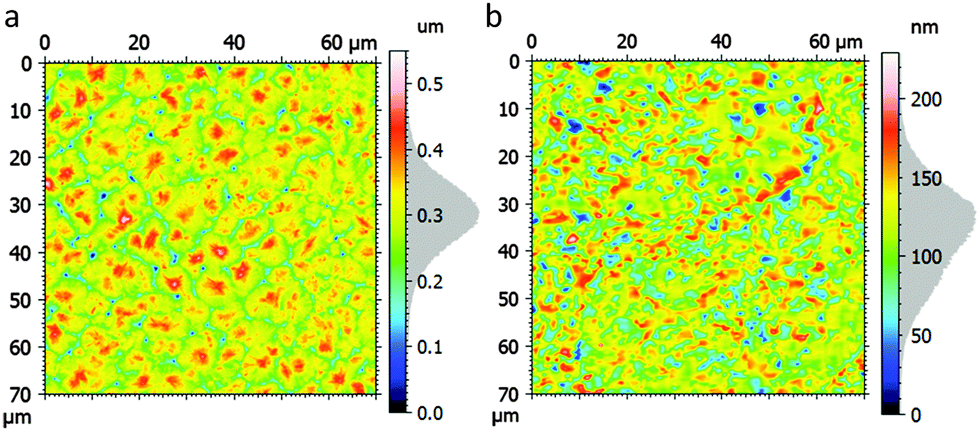 | ||
| Fig. 2 AFM height image of (a) PVDF layer (b) DB-TTF:PS layer. The RMS surface roughness is 53 nm and 28 nm respectively. The grey area on the scale bars displays the exact height distribution. | ||
Cr/Au source-drain electrodes (5 nm/35 nm thick respectively) were patterned on top of the PVDF layer by photolithography, evaporation and liftoff.
The surface of PVDF is highly hydrophobic and to improve surface wetting and achieve the subsequent deposition of the active layer, the sample was exposed to argon plasma in a reactive ion etcher at 100 mTorr, 50 W, for 30 s. No change in the surface roughness could be observed by AFM before and after the plasma exposure. Shorter exposure times can work though a wider OFET parameter spread is measured.
DB-TTF (Sigma Aldrich) was used without further purification and blended with polystyrene (3000 g mol−1) in a ratio of 1:3 in 4 wt% in anhydrous chlorobenzene and heated at 105 °C. The sample was placed on a coater bed at 105 °C, and a smooth bar located 0.3 mm above the sample sheared the solution forward at a speed of 10 mm s−1.
The thickness of the DB-TTF:PS layer was approximately 200 nm as measured by profilometry. In the films large DB-TTF crystallites can be seen by polarised optical microscopy (Fig. 1d). The roughness of the active layer is estimated to be 28 nm by AFM (Fig. 2b). To investigate the phase separation between the DB-TTF and the PS we utilised X-ray photoelectron spectroscopy (XPS) measurements (Fig. 3) to measure elemental composition as a function of distance from the surface. This was achieved by changing the incident angle, as at normal angles the penetration is higher than in grazing angles. The results show that within the first several nm from the surface, the carbon to sulphur ratio is slightly higher than in pure DB-TTF (3.8 measured, 3.5 in DB-TTF), and it increases with depth (4.6 at about twice the distance), indicating that the DB-TTF is mainly located at the top surface of the film, and the PS content increases with depth. This is consistent with the observations reported in our previous work of the DB-TTF:PS blend on SiO2.24 In that work it was also shown that the top DB-TTF layer is on the top but encapsulated by the PS, as pure DB-TTF is completely unstable under ambient conditions resulting in strong p-doping.24 X-ray diffraction measurements (Fig. S3, ESI†) show that DB-TTF crystallises in the γ-phase also as in previous work on SiO2.28 No X-ray peaks could be detected for PVDF.
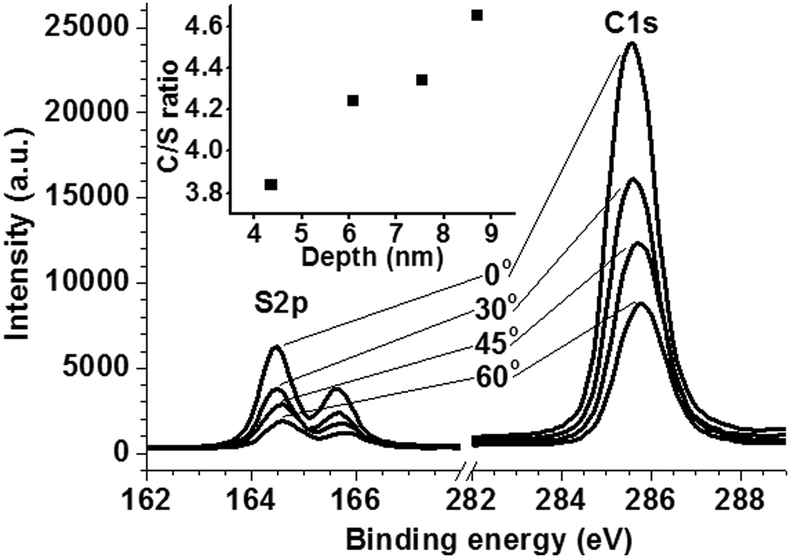 | ||
| Fig. 3 XPS spectrum of the DB-TTF:PS layer for different incidence angles. Inset: The carbon/sulfur ratio as a function of depth estimated from an inelastic mean free path of glassy carbon. | ||
The devices were characterised in air. The OFET shown in Fig. 4 exhibits an on/off ratio of 104, with peak saturation mobility of 0.2 cm2 V−1 s−1, VT of −2 V, subthreshold swing of 1.7 V per decade and hysteresis of 3.7 V extracted at VG = −5 V. Note that in the bidirectional transfer characteristic the current of the reverse sweep is higher than that of the forward sweep. This type of hysteresis originates from dielectric polarisation and not from the flow of mobile species along the semiconductor–insulator interface. It is typically observed in ferroelectric polymers such as PVDF, albeit it is much more pronounced for the higher crystallinity PVDF-TrFE copolymers utilised in memristors. The output characteristic at low VD is linear indicating efficient injection from the Au source/drain contacts (Fig. 4b). The reproducibility of the OFETs fabricated on the same substrate and on different substrates is very high (Fig. 4c and d). In 69 measured OFETs prepared on three different substrates, the average mobility was found to be centered at 0.2 cm2 V−1 s−1 and the VT at −1 V, with 100% of OFETs exhibiting values in the range of 0.1 to 0.4 cm2 V−1 s−1 and −2 to 0 V, respectively. The devices kept under ambient conditions did not show any degradation for over a week. The influence of bending on the electrical performance was also investigated. No significant variation was observed in the transfer characteristics, for inward and outward bending, in the direction parallel and perpendicular to the OFET channel, down to a bending radius of 5 mm (Fig. S4, ESI†). Also a unipolar inverter is demonstrated (Fig. S5, ESI†).
 | ||
| Fig. 4 (a) Forward and reverse transfer characteristic of an OFET with L = 50 μm, W = 4 mm, VD = −40 V. (b) Output characteristic for VG 0 to −40 V in steps of −5 V. (c) Peak saturation mobility and (d) threshold voltage spread from 69 OFETs on 3 different substrates. | ||
Conclusions
Flexible OFETs based on a low-cost, solution-processable PVDF insulator and a DB-TTF:PS semiconductor blend are demonstrated. Both the insulator and semiconductor layers are coated by highly scalable solution shearing techniques under ambient conditions. The PVDF layer exhibits high surface roughness. However, thanks to the fact that the subsequently deposited DB-TTF:PS blend vertically phase separates with a PS layer separating the PVDF and DB-TTF, the insulator surface is smoothened and depolarised. The OFETs are highly reproducible with a narrow mobility and threshold voltage spread, and mechanically stable down to an inward/outward bending radius of 5 mm.Acknowledgements
This work was mainly funded by the ERC StG 2012-306826 e-GAMES project. The authors also thank the Networking Research Center on Bioengineering, Biomaterials and Nanomedicine (CIBER-BBN), the DGI (Spain) with project BE-WELL CTQ2013-40480-R, and Generalitat de Catalunya 2014-SGR-17. We thank Dr M. Campoy for kindly allowing us to use his blade coater and Dr L. Morrone for valuable assistance with metal evaporation. F.G.D.P. thanks Universidad Técnica de Ambato and Secretaría de Educación Superior, Ciencia, Tecnología e Innovación for funding through a doctoral scholarship “Convocatoria abierta 2010”. We also acknowledge support of the publication fee by the CSIC Open Access Publication Support Initiative through its Unit of Information Resources for Research (URICI).References
- T. Sekitani, U. Zschieschang, H. Klauk and T. Someya, Nat. Mater., 2010, 9, 1015 CrossRef CAS PubMed; A. T. Zocco, H. You, J. A. Hagen and A. J. Steckl, Nanotechnology, 2014, 25, 094005 CrossRef PubMed.
- D. Elkington, N. Cooling, W. Belcher, P. C. Dastoor and X. Zhou, Electronics, 2014, 3, 234 CrossRef CAS.
- P. Lin and F. Yan, Adv. Mater., 2012, 24, 34 CrossRef CAS PubMed.
- G. Gelinck, P. Heremans, K. Nomoto and T. D. Anthopoulos, Adv. Mater., 2010, 22, 3778 CrossRef CAS PubMed; H. Sirringhaus, Adv. Mater., 2014, 26, 1319 CrossRef PubMed.
- K. Fukuda, Y. Takeda, M. Mizukami, D. Kumaki and S. Tokito, Sci. Rep., 2014, 4, 3947 Search PubMed.
- I. Doi, M. J. Kang and K. Takimiya, Curr. Appl. Phys., 2012, 12, e2 CrossRef.
- B. Kang, W. H. Lee and K. Cho, ACS Appl. Mater. Interfaces, 2013, 5, 2302 CAS.
- R. P. Ortiz, A. Facchetti and T. J. Marks, Chem. Rev., 2010, 110, 205 CrossRef CAS PubMed.
- M. Li, H. J. Wondergem, M. J. Spijkman, K. Asadi, I. Katsouras, P. W. M. Blom and D. M. De Leeuw, Nat. Mater., 2013, 12, 433 CrossRef CAS PubMed.
- S. W. Jung, S. M. Yoon, S. Y. Kang, I. K. You, J. B. Koo, K. J. Baeg and Y. Y. Noh, Curr. Appl. Phys., 2011, 11, S213 Search PubMed.
- A. Gerber, M. Fitsilis, R. Waser, T. J. Reece, E. Rije, S. Ducharme and H. Kohlstedt, J. Appl. Phys., 2010, 107, 124119 CrossRef.
- H. Sun, Q. Wang, Y. Li, Y. F. Lin, Y. Wang, Y. Yin, Y. Xu, C. Liu, K. Tsukagoshi, L. Pan, X. Wang, Z. Hu and Y. Shi, Sci. Rep., 2014, 4, 7227 CrossRef CAS PubMed.
- M. A. Khan, U. S. Bhansali and H. N. Alshareef, Adv. Mater., 2012, 24, 2165 CrossRef CAS PubMed.
- K. H. Lee, G. Lee, K. Lee, M. S. Oh and S. Im, Appl. Phys. Lett., 2009, 94, 093304 CrossRef.
- R. C. G. Naber, C. Tanase, P. W. M. Blom, G. H. Gelinck, A. W. Marsman, F. J. Touwslager, S. Setayesh and D. M. de Leeuw, Nat. Mater., 2005, 4, 243 CrossRef CAS.
- T. Kanashima, K. Yabe and M. Okuyama, Jpn. J. Appl. Phys., 2012, 51, 02BK06 CrossRef.
- R. H. Kim, H. J. Kim, I. Bae, S. K. Hwang, D. B. Velusamy, S. M. Cho, K. Takaishi, T. Muto, D. Hashizume, M. Uchiyama, P. Andre, F. Mathevel, B. Heinrich, T. Aoyama, D. E. Kim, H. Lee, J. C. Ribierre and C. Park, Nat. Commun., 2014, 5, 3583 Search PubMed.
- S. W. Jung, B. S. Na, K. J. Baeg, M. Kim, S. M. Yoon, J. Kim, D. Y. Kim and I. K. You, ETRI J., 2013, 4, 734 CrossRef.
- S. K. Hwang, S. Y. Min, I. Bae, S. M. Cho, K. L. Kim, T. W. Lee and C. Park, Small, 2014, 10, 1976 CrossRef CAS PubMed.
- R. C. G. Naber, M. Mulder, B. de Boer, P. W. M. Blom and D. M. de Leeuw, Org. Electron., 2006, 7, 132 CrossRef CAS.
- S. K. Hwang, T. J. Park, K. L. Kim, S. M. Cho, B. J. Jeong and C. Park, ACS Appl. Mater. Interfaces, 2014, 6, 20179 CAS.
- S. J. Kang, Y. J. Park, I. Bae, K. J. Kim, H. C. Kim, S. Bauer, E. L. Thomas and C. Park, Adv. Funct. Mater., 2009, 19, 2812 CrossRef CAS.
- J. Veres, S. D. Ogier, S. W. Leeming, D. C. Cupertino and S. M. Khaffaf, Adv. Funct. Mater., 2003, 13, 199 CrossRef CAS; A. F. Stassen, R. W. I. de Boer, N. N. Iosad and A. F. Morpurgo, Appl. Phys. Lett., 2004, 85, 3899 CrossRef.
- F. G. del Pozo, S. Fabiano, R. Pfattner, S. Georgakopoulos, S. Galindo, X. Liu, S. Braun, M. Fahlman, J. Veciana, X. Crispin, M. Berggren and M. Mas-Torrent, Adv. Funct. Mater., 2015 DOI:10.1002/adfm.201502274.
- M. Mas-Torrent, P. Hadley, S. T. Bromley, N. Crivillers, J. Veciana and C. Rovira, Appl. Phys. Lett., 2005, 86, 012110 CrossRef.
- T. Yamada, T. Hasegawa, M. Hiraoka, H. Matsui, Y. Tokura and G. Saito, Appl. Phys. Lett., 2008, 92, 233306 CrossRef.
- M. Kobayashi, K. Tashiro and H. Tadokoro, Macromolecules, 1974, 2, 158 Search PubMed.
- A. Brillante, I. Bilotti, R. G. D. Valle, E. Venuti, S. Milita, C. Dionigi, F. Borgatti, A. N. Lazar, F. Biscarini, M. Mas-Torrent, N. S. Oxtoby, N. Crivillers, J. Veciana, C. Rovira, M. Leufgen, G. Schmidt and L. W. Molenkamp, CrystEngComm, 2008, 10, 1899 RSC.
Footnote |
| † Electronic supplementary information (ESI) available. See DOI: 10.1039/c5tc02488a |
| This journal is © The Royal Society of Chemistry 2015 |