
 Open Access Article
 This Open Access Article is licensed under a
 Creative Commons Attribution 3.0 Unported Licence
Efficiency increase of organic solar cells with emissive light-in-coupling layers†
Beatrice
Beyer
*a and
Karl
Leo
b
aFraunhofer Institute for Organic Electronics, Electron Beam and Plasma Technology FEP, Maria-Reiche-Str. 02, 01109 Dresden, Germany. E-mail: beatrice.beyer@fep.fraunhofer.de
bTechnische Universität Dresden, Institut für Angewandte Photophysik (IAPP), George-Bähr-Str. 1, 01069 Dresden, Germany
First published on 18th September 2015
Abstract
Top-absorbing organic solar cells with a light incoupling layer allowing the exposure of harmful UV irradiation have been fabricated. Short-wavelength light is absorbed by the down-shifting system Alq3:DCM located in the light incoupling layer of top-absorbing organic solar cells and is converted into longer wavelengths. This red light is then absorbed by a ZnPc:C60 bulk heterojunction solar cell, showing a total power efficiency increase by more than 10% related to additional photocurrent generated by this architectural concept.
Introduction
Using photon conversion processes to positively influence the absorption behaviour is a common approach in the field of inorganic photovoltaics due to the discrete band structure of inorganic semiconductors. Photon conversion processes convert via luminescence parts of the solar spectrum to better match the absorption properties of a semiconductor device. ‘Multi-photon’ mechanisms such as up- and down-conversion, as well as single-photon processes like down-shifting can be used to achieve this goal.1,2Here, the excellent fluorescent properties of 4-(dicyanomethylene)-2-methyl-6-(p-dimethylaminostyryl)-4H-pyran (DCM) will be exploited to study the concept of internal downshifting of the solar light for organic solar cells. The aim is to modify the absorption profile of binary bulk heterojunction (BHJ) solar cells with fullerene C60 as an electron acceptor and zinc phthalocyanine (ZnPc) as an electron donor by utilizing the emission strength of DCM in the range between 580 and 780 nm. DCM will be inserted into the light incoupling layer (LIL) of top-absorbing solar cells in order to absorb light and to convert it into lower energy radiation, as presented in Fig. 1.
 | ||
| Fig. 1 Schematic presentation of the top-absorbing organic solar cell architecture (top left), the chemical structures of relevant compounds (top right) as well as their absorption and emission behaviour (bottom). | ||
Converting light of higher energy into lower energy by down-shifting is accompanied by a loss of photon energy and will result in a non-negligible degree of heating of the semiconductors due to the Stokes shift.1 However, this heating has to be dealt with for classical inorganic solar cells since the efficiency of these cells decreases at higher temperatures. This dependency of efficiency upon temperature is reversed for organic solar cells.3–5 So, the introduction of a down-shifting emitter molecule does not just convert the solar spectrum, it can also heat the cell from the inside. For our investigations the down-shifting emitter DCM is placed in the light incoupling layer conventionally consisting of pure tris(8-hydroxyquinolinato)aluminium (Alq3) within the optoelectronic device without lowering the overall electrical performance of the bulk heterojunction (BHJ) organic solar cells (OSCs) by affecting also the fill factor (FF) or open circuit-voltage (VOC), as often observed when sensitizers are added to the BHJ such as in ternary bulk heterojunction solar cells.6,7
Experimental
Sample preparation
Solar cells were fabricated by a consecutive (co-)evaporation of organic materials in a custom-made organic material beam deposition tool (Bestec, Germany) at a pressure of 10−8–10−7 mbar and at room temperature. A pre-cleaned bare glass (Luminescence Technologies) was used as a substrate. We used a p–i–n device architecture in order to provide ohmic contacts to both electrodes.8 The active layer (ZnPc:C60, materials were twice sublimed prior to utilization) was embedded between an anode consisting of 50 nm aluminum and 30 nm silver, a p-doped hole transport layer (HTL) of 2,2′,7,7′-tetra(m-tolyl-phenylamino)-9,9′-spiro-bifluorene (spiro-TTB) in varied thicknesses and a 20 nm thick blocking layer of C60 (BL), followed by an n-doped electron transporting layer of 15 nm C60 (ETL) and a cathode of 3 nm aluminium and 12 nm silver. For processing reasons, p- and n-doping was done employing the proprietary molecular dopant NDP9 and NDN26 (Novaled AG, Germany), which could be replaced by the open materials 2,3,5,6-tetrafluoro-7,7,8,8-tetracyanoquino-dimethane (F4-TCNQ) and Cs2CO3, respectively. For the specific investigations (HTL thickness variation, DCM dopant concentration variation) all samples and layers were fabricated within one single deposition run by either applying a wedge tool (for HTL thickness increase without interrupting the process) or specially structured shadow masks (for doping variation). Each OSC sample obtained four pixels with an active area of 4.5 × 5 (mm)2 for characterisation to investigate the statistical deviation.Sample characterisation
J–V measurements (Keithley 2400 source meter, Kepco power supply) are recorded under dark conditions and under AM1.5 and 100 mW cm−2 illumination (KHS Technical lighting) at 25 °C. The optical constants were determined by transmission and reflection spectroscopy (Solid Spec, Shimadzu) and by subsequent data fitting with the software WVASE32 (J.A.Woollam Co., Inc.). Spectral response curve data were recorded using a spectrofluorometer (Horiba Jobin Yvon, Fluoromax-4, also used for photoluminescence measurements) calibrated with a Si photodiode and a Keithley 2400 source meter. Along with the short current density (JSC), the fill factor (FF), open circuit voltage (VOC), and power efficiency (η), the saturation (S) is given, defined as the current density ratio at −1 V and 0 V (S = J(−1 V)/JSC).Optical simulations
In order to investigate the field distribution in optoelectronic devices, the simulation software Setfos 3.2 (Fluxim, Switzerland) was used. Optical constants were determined by transmission and reflection spectroscopy. The field amplitudes and the energy fluxes for each wavelength, at each position within the stack were calculated by using a transfer matrix formalism implementing the optical constants of each layer. For optimization of the transport layer thicknesses, the absorptivity of the absorption layer was maximized for the AM1.5 solar spectrum.Results and discussion
Optical properties of Alq3:DCM
DCM has widely been used as an emitter dopant material with Alq3 as a host system in organic light emitting diodes (OLEDs). Remarkably, DCM shows a distinct solid solvation dependency in Alq3.9 This effect is expressed in the form of a concentration dependent emission colour and intensity. The more emitter is doped into Alq3, the more the emission is bathochromically shifted. This has been ascribed to the self-polarization of the DCM molecule, since it is more polar than the average organic semiconductor material or Alq3, respectively. Because of this dependence of emission upon concentration, thin films with different DCM concentrations were fabricated and characterized. Fig. 2a shows the transmission spectra of various Alq3:DCM thin films with different compositional ratios. The more DCM is added, the stronger the transmission at around 495 nm is reduced; this is due to the increasing absorption of DCM. Fig. 2b shows the PL spectra of these layers excited at 495 nm for various DCM contents. As mentioned before, the emission shows a bathochromic shift due to the increasing polarity with rising DCM content. After reaching a doping concentration of 10 wt%, the emission is not further red-shifted. Additionally, the emission originating from Alq3 is immediately reduced after the addition of DCM. This is a clear sign of an efficient Förster resonance energy transfer (FRET). In order to investigate the excitation and emission characteristics of pure Alq3 and DCM-doped Alq3, emission spectra have been recorded for excitation wavelengths between 270 and 480 nm. These 3D spectra are presented in Fig. 2c and d for pure and doped Alq3, respectively. In both graphs the emission has been measured from 500 to 800 nm, where it matches with the C60:ZnPc absorption of BHJ OSCs. The spectrum of pure Alq3 is characterized by green emission which exhibits its lowest energy excitation maximum at 370 nm. It can be seen that the wavelength of the emission maximum increases with rising excitation wavelength, whereas it stays almost unchanged in the doped Alq3 thin film. The emission in this case is characterized by a red colour with high intensity. The existence of FRET is attested to the unchanged location of the lowest energy excitation maximum at around 368 nm, which means that the energy absorbed by Alq3 is directly transferred to the energy acceptor molecule DCM. Beyond the excitation of Alq3, DCM still emits by itself with a slightly lower intensity. Thus, red emission can be realized by excitation between 270 and 550 nm.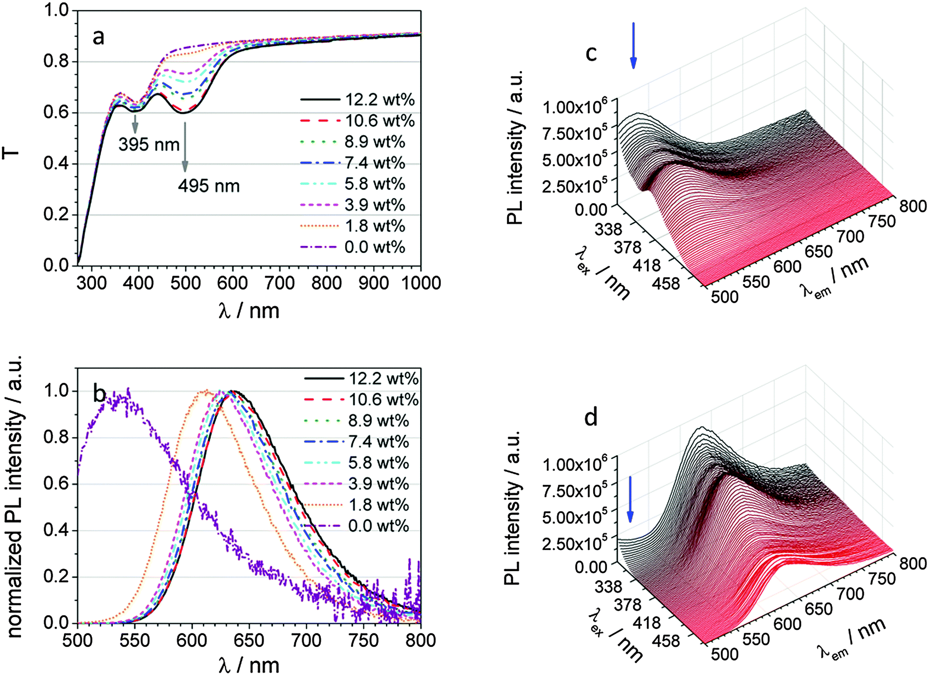 | ||
| Fig. 2 Transmission (a) and normalized PL spectra (b) of 80 nm Alq3:DCM thin films depending on the DCM concentration as well as 3D photoluminescence spectra of thin films of pure Alq3 (c) and Alq3 doped with 10 wt% DCM (d). | ||
Light incoupling layers are used to influence the optical field distribution and its amplitude, and to reduce the external reflection of the semitransparent top contact. Whereas a strong correlation between the LIL and the JSC exists, Meiss et al. described minor influences on the VOC, FF, and saturation values.10 Because of the convenient possibility of tuning the emission colour by varying the doping concentration, this LIL can be adjusted for several electron donor systems of the active solar cell layer absorbing between 500 and 700 nm. Furthermore, with the combination of DCM and Alq3, another advantage arises. Pure Alq3 has a large absorption coefficient (α > 105 cm−1 from 250 to 300 nm, α > 104 cm−1 from 300 to 420 nm) in the UV to blue range while staying below 10−1 cm−1 for longer wavelengths. This means that more than a half of the near-UV light is absorbed by a film of only 40 nm thickness.
Additionally, pure Alq3 shows a green emission, whose intensity is, however, still two magnitudes lower than the doped film, thus rather weak. Due to the strong absorption between 300 and 440 nm, the energy rich UV/vis radiance, often attributed to the degradation of several organic semiconductors in organic solar cells, is filtered out before the organic solar cell.11 Adding DCM into Alq3 broadens the absorption range of energy rich radiance to 550 nm, although it is not anticipated for this experiment. Additionally, the energy is not lost for the solar cell as it would be the case for pure Alq3. The absorbed light with a wavelength as short as 400 nm will be transferred from Alq3 to DCM via FRET, resulting in radiative decay as red emission. This can easily be absorbed by the C60:ZnPc containing absorption layer of OSCs, as shown by the spectral overlap of Alq3:DCM emission with C60:ZnPc absorption. The normalized spectra (cf. ESI,† S1) have an overlap of 99.5%.
Optical simulations
In order to apply a fluorescent LIL in organic solar cells, a stack architecture for top-absorbing solar cells is utilized. The principle architecture has been adopted from ref. 10 but has been modified. Several optical simulations have been carried out in order to locate the electric field amplitude maximum in the absorption layer as it is of great interest for solar cells in top-absorbing geometry.12,13 The optical simulations started with a fixed stack architecture, and the variation was carried out for each layer. The results are presented in the supplementary information for pure Alq3 (ESI,† S2) and doped Alq3 (ESI,† S3) as a LIL material. The absorptivity of C60:ZnPc shows a dependency upon all layers in the spectral region from 550 to 750 nm, however with different sensitivities. Whereas the thicknesses of the BL, ETL and HTL have an enormous impact on the position of the optical cavity, the influence of the LIL is comparatively low. For clarification, the predicted JSC under the assumption of AM1.5 illumination is illustrated, too. It has to be noted that the impact of emissive layers could not be considered in these simulations.Due to the parasitic absorption of the BL and ETL, their thicknesses were limited for simulations revealing only the first field amplitude maximum. However, because of processing reasons, the second thickness maxima were not considered for the HTL and LIL. Furthermore, it can be seen that a thin semitransparent cathode is essential for high JSC values. Hence, a thickness for an optimal compromise between high transparency and good conductivity should be chosen.
The simulations for pure and doped Alq3 as light incoupling layers show that the dopant (concentration) has only a minor influence on the generated photocurrent, although the optical behaviour of the LILs is rather different (cf. S4 and S5, ESI†).
Because of the good agreement between the pre-assumed stack architecture and the simulation results, only the thickness of the HTL was experimentally varied for optimization purposes. Hence, an organic solar cell consisting of the following layer sequence will be investigated: a glass/opaque anode of aluminium and silver/x nm p-spiro-TTB, a 35 nm AL/20 nm BL/15 nm ETL/15 nm cathode of aluminium and silver/80 nm LIL. Since the emissive LIL and the absorbing AL are separated by around 50 nm, which is too large for FRET, the magnitude of the incoupling will be investigated by a variation of the DCM concentration in the LIL to directly study the effect of this approach.
Variations in the HTL thickness
As summarized in the ESI,† (S2, S3), the dependency of high photocurrents on thickness is most pronounced for the HTL. A continuous increase of the AL thickness has led to a significant drop in FF and was kept at 35 or 40 nm. Thus, samples with seven different HTL thicknesses ranging from 45 to 90 nm were fabricated in order to investigate the best thickness to enable high JSC values. Table 1 gives an overview of the resulting key values of the devices. As expected, FF and VOC show no significant dependency on the HTL thickness. This is attributed to the high conductivity of the p-HTL, preventing charge carrier losses due to high resistance. However, the scattering of the values is higher than expected from the evaluated measurement uncertainty. Nonetheless, a clear relation between JSC and the HTL thickness can be drawn. Fig. 3a and b present the measured J–V curves in the dark and under illumination and shows the evaluated dHTL–JSC relation in comparison with the predicted JSC values from the optical simulations. Clearly, JSC has a maximum for thicknesses in the range between 65 and 80 nm and the results are consistent with the predicted behaviour. According to the simulations, a maximum short circuit current density is reached for an HTL thickness of 65 nm. The experiments show that slightly higher thicknesses also give very good photocurrents. This reproduction shows that the optical model used as well as the applied parameter sets of the optical constants are in good agreement with reality.| d HTL/nm | V OC/mV | J SC/mA cm−2 | FF/% | η/% | S |
|---|---|---|---|---|---|
| 45 | 503 ± 9 | 4.23 ± 0.07 | 48 ± 0.5 | 1.03 ± 0.02 | 1.18 ± 0.02 |
| 55 | 508 ± 13 | 5.20 ± 0.08 | 49 ± 0.5 | 1.31 ± 0.03 | 1.21 ± 0.02 |
| 60 | 506 ± 12 | 5.40 ± 0.07 | 49 ± 0.5 | 1.35 ± 0.02 | 1.15 ± 0.02 |
| 65 | 536 ± 14 | 5.63 ± 0.07 | 45 ± 0.4 | 1.36 ± 0.02 | 1.15 ± 0.02 |
| 70 | 516 ± 11 | 5.61 ± 0.08 | 46 ± 0.5 | 1.36 ± 0.03 | 1.17 ± 0.02 |
| 80 | 538 ± 14 | 5.58 ± 0.06 | 47 ± 0.5 | 1.42 ± 0.02 | 1.17 ± 0.02 |
| 90 | 519 ± 8 | 4.84 ± 0.07 | 43 ± 0.4 | 1.10 ± 0.02 | 1.21 ± 0.02 |
 | ||
| Fig. 3 J–V characteristics of top-absorbing OSCs under illumination (line + symbol) and in the dark (line) depending on the hole transport layer (HTL) thickness (a) and concentration of DCM doped in Alq3 (c) as well as their JSC values plotted against the thickness (b) in comparison with the predicted values from simulations and against the DCM concentration (d). | ||
Impact of the DCM concentration within the LIL
In order to validate the justification of the DCM insertion into the LIL, the DCM concentration was varied from 0 to 10 wt%. The J–V curves recorded under illumination and in the dark of the resulting OSC (cf.Fig. 3c and d) show samples with high fill factors and VOC values as expected for C60:ZnPc BHJ cells. The key values of the resulting devices are summarized in Table 2. Since the LIL is not involved electrically in the photovoltaic processes, parameters such as the FF, VOC, and S are not significantly affected by the dopant concentration. Merely the short-circuit current density JSC increases with rising DCM content in the LIL. Starting with the top-absorbing sample with pure Alq3 as a LIL material, short circuit current densities of 7.20 mA cm−2 are obtained yielding an efficiency of 1.90%, which is slightly higher than reported by Meiss and co-workers for a comparable architecture (1.84%).10 After adding DCM to Alq3 by co-deposition, the emission intensity of the LIL increased and changed from greenish to orange-reddish; the BHJ absorption layer can better absorb the red light re-emitted by the LIL. This is confirmed by the EQE measurements, which will be discussed later in detail. Interestingly, the enhancement of the photosensitivity saturates quickly, as displayed in Fig. 4b. The highest jump of 0.41 mA cm−2 is observed at 2% DCM addition. Addition of further DCM to a dopant concentration of 6% enhances JSC by 0.21 mA cm−2, and after another 4% DCM (a total content of 10%) only by 0.12 mA cm−2.| C DCM/% | V OC/mV | J SC/mA cm−2 | FF/% | η/% | S |
|---|---|---|---|---|---|
| 0 | 514 ± 7 | 7.20 ± 0.09 | 51 ± 0.5 | 1.90 ± 0.02 | 1.21 ± 0.02 |
| 2 | 524 ± 7 | 7.61 ± 0.08 | 53 ± 0.4 | 2.11 ± 0.02 | 1.19 ± 0.02 |
| 6 | 537 ± 8 | 7.80 ± 0.08 | 52 ± 0.4 | 2.16 ± 0.03 | 1.19 ± 0.02 |
| 10 | 525 ± 6 | 7.92 ± 0.09 | 53 ± 0.4 | 2.21 ± 0.02 | 1.19 ± 0.02 |
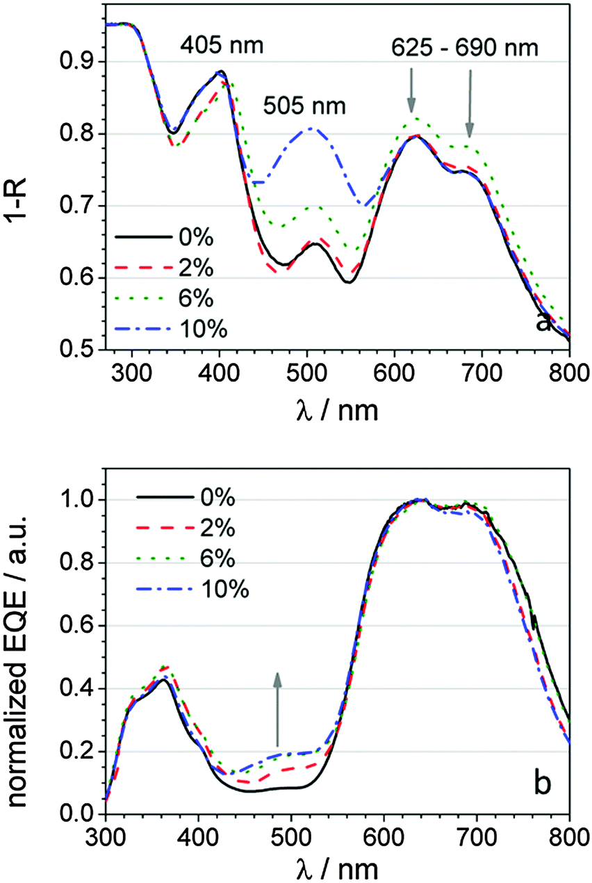 | ||
| Fig. 4 (a) Absorption spectra of the devices as well as (b) their corresponding normalized EQE measurements depending on the DCM concentration in the light incoupling layer. | ||
In order to analyse these results further, reflectance and emission spectra have been recorded for these samples. By means of the reflectance spectra, the absorption of the whole device can be evaluated. As displayed in Fig. 4a, the absorption peaks originating from Alq3 (405 nm), DCM (505 nm) and ZnPc (625–690 nm) can be assigned. Whereas the absorption stays nearly unchanged for Alq3 and ZnPc related bands, the DCM band increases noticeably with rising dopant concentration, which results, for the sample with 10% DCM in the LIL, to an absorption value comparable to that of the ZnPc band. These measurements show that the absorption profile of the devices can be considerably altered by the choice of the LIL composition.
However, there is often a huge difference between the absorption capability and the generation of free charge carriers. Unlike the absorption spectra, the EQE spectra show the dominant Q/Q+ bands of ZnPc and the superposition of C60 and Alq3 absorption. For clarification, the spectra are normalized at the ZnPc related bands because all the layers beyond the LIL have been kept equal. At 480 nm an absorption shoulder rises and increases with DCM content. For the interpretation of the EQE spectra, a discussion of the emission properties of the light incoupling layers is required.
The PL spectra of all solar cell samples are presented in Fig. 5 and show the emission spectra of all four samples at various excitation wavelengths. These wavelengths have been selected to correspond to shoulders or maxima in the EQE spectra. Depending on the excitation wavelength, transitions occurring in either Alq3 (330, 365 and 405 nm) or DCM (480 nm) are excited. The device with pure Alq3 has a yellowish emission with rising intensity for longer excitation wavelengths. Emission in the red region is not observed. After inserting 2% DCM into Alq3, all the excitation energy is transferred to the DCM molecule via FRET, resulting in red emission. Furthermore, the DCM molecule can also be directly excited by illuminating it with 480 nm light. Further addition of DCM to 6% has increased the emission intensity and shifts it slightly bathochromically. Beyond that, the direct excitation of DCM becomes more effective. This observation continues to be true up to a content to 10%. The highest intensity of red light is achieved after direct excitation of DCM, for which the energy transfer from Alq3 is less efficient compared to lower DCM concentrations.
 | ||
| Fig. 5 PL spectra of top-absorbing OSCs with different LILs in variation of their DCM doping concentration (0–10%). These spectra are depicted for the excitation wavelengths at 330 nm (line), 365 nm (dashed), 405 nm (dotted) and 480 nm (dash-dotted). | ||
A comparison between these results and the EQE spectra (Fig. 4b) explains the steep increase of the short circuit current density after the insertion of 2% DCM into the LIL and the subsequent saturation. The emission from pure Alq3 is green and can hardly be absorbed by ZnPc. Due to the effective FRET from Alq3 to DCM, photon energy absorbed by DCM and most notably by Alq3 can be utilized for exciton generation in the C60:ZnPc blend because of the matching spectral overlap between the red DCM related emission and the absorption profile of ZnPc. Up to 6% of DCM, the effectivity of this FRET and the emission intensity increase with doping concentration. This can be seen in the EQE spectra with a higher sensitivity at 360 nm (Alq3 excitation) and 480 nm (DCM excitation). At 10% DCM content, the sensitivity at 360 nm drops back to a value prior to DCM doping and reveals only a higher response at 480 nm, which means that mainly direct excitation of DCM occurs. Hence, higher DCM concentrations in the LIL will not increase the JSC value further. The solar energy irradiated from 300 to 420 nm yields only 71 mW m−2 nm−1 and increases up to 247 mW m−2 nm−1 within the spectral range of 300 to 540 nm, which is around the half of the spectral range from 300 to 800 nm with 589 mW m−2 nm−1. Thus, enhancing the absorptivity in the blue range of light can only account for 12% of the achievable energy from 300 to 800 nm. Addressing also the part of the spectrum till 540 nm, already 42% of the irradiated energy is available for charge generation. Keeping this in mind, the JSC improvement resulting from the addition of 2% is with 0.4 mA cm−2 (5%) remarkable and maximizes at 10 wt% by 0.72 mA cm−2 (10%), although becomes less efficient due to direct absorption of DCM.
However, since the doped LIL has the main purpose of accessing filtered UV light (∼300 to 400 nm), the absorption increase at around 500 nm can be considered as parasitic since broader absorbing solar cell systems would negatively be influenced and result in lower power conversion efficiencies. From this aspect, the sample with only 2% DCM in Alq3, but predominantly only contributing by Alq3 absorption represents the best choice.
In order to increase the positive contribution of the emissive LIL further, a special layer design could be applied where less than 50% of the LIL emission is directed out of the solar cell into the air. This could be realized by an anisotropic orientation of the dopant emitter or increasing the reflectivity of the LIL/air interface.
Conclusions
We present organic solar cells which harvest the higher energy part of sun light more effectively by applying an emissive light incoupling layer on a top-absorbing cell structure. Due to the efficient down-shifting properties of Alq3:DCM, the overall power efficiency has been increased by 10% (with 2% DCM in Alq3) and demonstrates that emission can effectively be absorbed within this optoelectronic device architecture when the spectral match between the emissive LIL and the absorbing BHJ layer is large.Acknowledgements
Richard Pfeifer is acknowledged for his support with the optical simulations and related discussions.Notes and references
- R. Koeppe, O. Boassart, G. Galzaferri and N. S. Sariciftci, Sol. Energy Mater. Sol. Cells, 2007, 91, 155 CrossRef PubMed.
- S. Iijima, F. Mizutani and Y. Tanaka, Bull. Chem. Soc. Jpn., 1985, 58, 1585 CrossRef CAS.
- E. A. Katz, D. Faiman, S. M. Tuladhar, J. M. Kroon, M. Wienk, T. Fromherz, F. Padinger, C. J. Brabec and N. S. Sariciftci, J. Appl. Phys., 2001, 90, 5343 CrossRef CAS PubMed.
- I. Riedel, J. Parisi, V. Dyakonov, L. Lutsen, D. Vaderzande and J. C. Hummelen, Adv. Funct. Mater., 2004, 14, 38 CrossRef CAS PubMed.
- A. S. Riad, S. M. Khalil and S. Darwish, Thin Solid Films, 1994, 249, 219 CrossRef CAS.
- J.-S. Huang, T. Goh, X. Li, M. y. Sfeir, E. A. Bielinski, S. Tomasulo, M. L. Lee, N. Hazari and A. D. Taylor, Nat. Photonics, 2013, 7, 479 CrossRef CAS PubMed.
- T. Ameri, P. Khoram, J. Min and C. J. Brabec, Adv. Mater., 2013, 25, 4245 CrossRef CAS PubMed.
- B. Maennig, D. Gebeyehu, P. Simon, F. Kozlowski, A. Werner, F. Li, S. Grundmann, S. Sonntag, M. Koch, K. Leo, M. Pfeiffer, H. Hoppe, D. Meissner, N. Sariciftci, I. Riedel, V. Dyakonov, J. Parisi and J. Drechsel, Appl. Phys. A: Mater. Sci. Process., 2004, 79, 1 CrossRef CAS.
- V. Bulovic, A. Shoustikov, M. A. Baldo, E. Bose, V. G. Kozlov, M. e. Thompson and S. R. Forrest, Chem. Phys. Lett., 1998, 287, 455 CrossRef CAS.
- J. Meiss, M. Furno, S. Pfuetzner, K. Leo and M. Riede, J. Appl. Phys., 2010, 107, 053117 CrossRef PubMed.
- M. Hermenau, M. Riede and K. Leo, Stability and Degradation of Organic and Polymer Solar Cells, ed. F. C. Krebs, Wiley-VCH, 2012 Search PubMed.
- H.-W. Lin, S.-W. Chiu, L.-Y. Lin, Z.-Y. Hung, Y.-H. Chen, F. Lin and K.-T. Wong, Adv. Mater., 2012, 24, 2269 CrossRef CAS PubMed.
- H.-W. Chong, J. Lee, S. Hofmann, Y. H. Kim, L. Müller-Meskamp, B. Lüssem, C.-C. Wu, K. Leo and M. C. Gather, J. Appl. Phys., 2013, 113, 204502 CrossRef PubMed.
Footnote |
| † Electronic supplementary information (ESI) available: Spectral overlap of Alq3:DCM and ZnPc:C60; results of optical simulations for various layers and thicknesses; optical constants of Alq3 and Alq3:DCM. See DOI: 10.1039/c5tc02446c |
| This journal is © The Royal Society of Chemistry 2015 |