
 Open Access Article
 This Open Access Article is licensed under a
 Creative Commons Attribution 3.0 Unported Licence
Influencing FTO thin film growth with thin seeding layers: a route to microstructural modification†
Nuruzzaman
Noor
,
Clair K. T.
Chew
,
Davinder S.
Bhachu
,
Matthew R.
Waugh
,
Claire J.
Carmalt
and
Ivan P.
Parkin
*
Materials Research Centre, UCL Department of Chemistry, Christopher Ingold Building, 20 Gordon Street, London, WC1H 0AJ, UK. E-mail: i.p.parkin@ucl.ac.uk; Fax: +44 (0)20 7679 7463; Tel: +44 (0)20 7679 4669
First published on 24th August 2015
Abstract
We report on the seeded growth of fluorine doped tin oxide (FTO) polycrystalline transparent conducting oxide (TCO) thin films on float glass using a novel two-step chemical vapour deposition (CVD) method. Aerosol-assisted CVD (AACVD) was used to grow a seed layer to direct and promote full film growth via an atmospheric pressure CVD (APCVD) overlay. The method allowed for reproducible control over morphology and denser, rougher, higher-performing TCO at a relatively low growth temperature (500 °C). Growth promotion depended on seeding time with an optimal seeding time being present, below which morphology control and conformal coverage was unavailable. The film properties and functional characteristics were characterised by SEM, AFM, XRD, XPS, UV-Vis-Near IR transmittance-reflectance and Hall Effect probe measurements. Highly transparent and electrically conductive films, comparable to commercial materials and with high roughness and low transmission haze values indicate the process yields high quality films with a controllable morphology that can be tuned to desired application. The versatile method provides a route towards the morphological control of high-quality FTO thin films with high optical clarity and low-emissivity properties and can be readily extended to a variety of different substrates and metal oxide materials.
1 Introduction
Transparent conducting oxides (TCO) are thin film materials that are simultaneously optically transparent and appreciably electrically conductive. This extremely valuable coincidence of properties means TCO find use in a wide variety of applications including for glazing, flat panel displays and solar panels, usually as electrodes.1 Doped SnO2 based TCO are some of the most widely used transparent conducting materials (TCM), the intrinsically n-type semiconducting properties further enhanced through selective aliovalent doping to obtain highly conductive, transparent thin films.2–8As technologies continue to advance, demands on the hardware, including TCO components, are increasing. Unfortunately, the limits imposed on TCO properties due to the competitive nature of the underlying electrical and optical mechanisms in such films mean the limits of raw electrical conductivity or optical transparency property improvements are fast being reached.9,10 Future performance advances for conventional TCO will require more sophisticated methods for effecting property improvements, such as more precise tailoring of film properties to specific applications, in addition to the exploration of less conventional TCO frameworks, e.g.; doped TiO2.11–18 The former includes the control of secondary properties through, for example, film preferred orientation to minimise charge carrier obstacles and tune morphology so as to best suit the optical scattering needs of an application. The effective use of nanostructured components for novel technologies requires the ability to design and synthesise materials with highly controlled surface features in a reproducible manner.19 Since the physical properties of a polycrystalline thin film generally depend on its crystallographic features, especially crystallographic orientation and grain size,20 the optimisation of surface texture, which can be controlled by the use and variation of nucleating seed layers, is commercially important for fully utilising these strongly anisotropic properties. Different TCO microstructural feature sizes lead to different interactions with light including in-coupling, light trapping and absorbance.21–23 Such morphological features are important for secondary optical characteristics such as haze (the amount of light diffusely scattered overall due to angled surface features), the control of which is important so as to tune growth to different application, e.g.; silicon solar cell layers vs. optoelectronic layers, or for use in suspended particle devices (SPD).24–26
The production of fluorine-doped SnO2 (FTO) – one of the worlds most widely used and produced TCO – and other conventional TCO is frequently carried out by atmospheric-pressure chemical vapour deposition (APCVD), most notably by Pilkington-NSG for their TEC glass range.27–29 APCVD involves the use of discrete chemical precursors, the concentration of which is controlled by gas flows prior to mixing and the subsequent deposition for film formation, to control functional properties.30 However, whilst optimised electrical conductivity and optical transmittance TCO values can be achieved using this high-throughput deposition method, control of microstructure, particularly the various morphologies afforded by techniques such as aerosol-assisted CVD (AACVD), cannot be reproduced due to the lack of growth control on the amorphous glass substrate. AACVD is a solution processing method that can deliver single source precursors (i.e.; all required thin film components are present at the desired ratios in a precursor mixture) to a heated substrate in the form of an aerosol and has been used for a variety of materials syntheses.4–6,31–38 Both the uniformity of the precursor mixture and small size distribution of aerosol particles results in a highly uniform thin film, although the longer deposition times required due to the slower aerosol delivery rate limit its ability to be easily engineered into a glass production line. Despite the variant delivery methods, both APCVD and AACVD involve vapourisation of the precursor chemicals immediately prior to deposition and thin film formation. Thus, a method to incorporate the desirable and tunable properties as afforded by AACVD with the speed of the industrially friendly APCVD method would be extremely beneficial.
This study looks at the use of a light, randomly orientated seeding layer to provide nucleation points from which APCVD growth can proceed.39–41 Those nucleation sites, as synthesised by AACVD, exhibit texture control and increased film density due to the promotion of homo-epitaxial nucleation and growth versus direct growth on an amorphous glass substrate. Thus, the seeding layer should nucleate growth, giving variant grain growth characteristics compared to conventional APCVD thin films due to a reduced film growth induction time, by providing a lower activation energy barrier to improved film formation, yielding denser, faster growing and more adhesive films.42,43 Additionally, the films formed have more uniform grain sizes and grain boundaries; important for improved thin film technology,44 as well as greater control over feature shape and size, which will have important implications for incident light scattering and so TCO application.45,46 Seeding strategies have been similarly used to good effect in the formation and control of microstructures in a variety of materials.20,46–57
The work presented in this paper explores FTO synthesis by the AA-AP CVD seed-overlay method. The data illustrates how increasingly controllable morphologies are possible solely through the use of a seed layer and will have important implications in future FTO synthesis and thin film morphology manipulation.
2 Experimental
All chemicals were used as bought; butyltintrichloride (MBTC; 95%; Sigma-Aldrich), trifluoroacetic acid (TFA; 98%; Sigma Aldrich), methanol (MeOH; ≥99.5%, Analar), ethyl acetate (EtOAc; ≥99.5%, Analar) and deionised water. Compressed air was obtained through a house line fitted with a filter. The glass substrate for deposition was 3.2 mm thick plain float glass with a 50 nm thick SiO2 barrier layer, as supplied by Pilkington NSG.2.1 Synthesis
AACVD (see Fig. 1) was carried out in a flat-bed, cold-walled tubular reactor, as described elsewhere.33,38 Substrates were cleaned with soap, water, isopropanol and acetone then allowed to dry under air ambient prior to loading into the reactor. The AACVD precursor solution was made by mixing MBTC (0.2 mol dm−3), MeOH and TFA. Depositions were carried out on barrier coated float glass substrates measuring 145 mm × 45 mm × 3.2 mm (length × width × thickness). Substrates were heated to the desired temperature before deposition, the film deposited at 500 °C using compressed air (constant 2 bar pressure) and cooled under air to room temperature. A pneumatic aerosol generation method was applied, using a TSI Model 3076 Constant Output Atomiser, over a range of deposition times. | ||
| Fig. 1 Illustrative schematic of an AACVD deposition reactor set-up. | ||
APCVD (see Fig. 2) was carried out in a flat-bed, cold-walled tubular reactor, as described elsewhere.33 The seeded substrates were manually transferred in from the AACVD reactor once cool, to the APCVD reactor, without any further treatment. SnO2 based films were formed from the reaction of MBTC and EtOAc alongside the TFA fluorine-dopant precursor. MBTC is one of the most widely used SnO2 precursors due to its ease-of-use and it readily volatolises in a CVD bubbler, decomposing cleanly during deposition to give high-quality TCO films. EtOAc is required because SnO2 synthesis often requires an oxidant source in order to help formation of the oxide.
 | ||
| Fig. 2 Illustrative schematic of an APCVD deposition reactor set-up. | ||
In each experiment, precursor reagents were volatilized in isolated heated bubblers (MBTC and EtOAc) or introduced via a syringe (TFA in H2O; 5 vol%) and then transported to the mixing chamber by inert plain line flow of N2 carrier gas, which in turn passed into the heated reactor via a baffle manifold. Depositions were carried out on FTO-seeded barrier coated float glass substrates measuring 145 mm × 45 mm × 3.2 mm (length × width × thickness). Films were cooled to room temperature under a stream of N2 after deposition. The resistivity, ρ, at a number of positions on each film was screened, allowing identification of the position of minimal electrical resistivity. Only those conditions used to form the region of lowest ρ across the series are discussed for each seed-overlay deposition system.
2.2 Analysis
X-ray diffraction (XRD) measurements of the synthesised films were made in ambient air on a LynxEye D8 diffractometer with readings taken over a 21–66° 2θ range. Diffraction patterns were analysed for crystallinity, orientation and phase purity. Patterns were fit to a Le Bail refined model using GSAS EXPGUI software and crystallite sizes extracted from the Lorentzian broadening term.57,58 X-ray photoelectron spectroscopy (XPS) analysis was carried out using a Thermo Scientific K-Alpha spectrometer with monochromated Al Kα radiation, depth profiling 16 levels, at 20 second intervals, followed by readings, with a 10 second pause before acquisition (an experimentally determined sputter rate of approximately 0.7–0.8 nm s−1). Survey scans were collected in the range of 0–1200 eV at 200 eV pass energy. High-resolution spectra were acquired at 50 eV pass energy and used for the principal peaks of Sn (3d), O (1s), F (1s), and C (1s). The area underneath these bands is an indication of the concentration of element within the region of analysis (spot size 400 μm). Peaks were modelled with CASAXPS using relative sensitivity factors to calculate the film composition and referenced to adventitious carbon at a binding energy (B.E.) of 284.8 eV. All Room temperature Transmittance–Reflectance (T–R) profiles were taken using a Perkin Elmer Fourier Transform Lambda 25 UV-Vis-Near IR spectrophotometer over a wavelength range of 200–2500 nm against an air background. The bandgap was derived from Tauc plots of data in transmission. Transmission haze measurements were carried out on a BYK-Gardner Haze-Gard at the Pilkington NSG site. Scanning Electron Microscopy (SEM) images were obtained using a JEOL JSM-6301F Field Emission SEM at 5 keV accelerating voltage. Room temperature Hall Effect measurements were carried out on an Ecopia HMS-3000 using a current of 1 mA and 0.58 T magnetic field, utilising measured film thickness values as obtained from a Filmetrics F20 spectral reflectance system in air against an as – supplied FTO standard. Ohmic contacts were formed with indium–tin solder and tested on the in-built software prior to measurement. Raman spectroscopy measurements were carried out on a Renishaw 1000 in via UV-Vis spectrometer utilising a green laser (514 nm) under ambient conditions. AFM imaging was carried out on a Nanosurf Easyscan 2 Controller in contact mode and surface roughness properties calculated. Images were visualised using the Gwyddion software and zeroed.593 Results and discussion
3.1 Film synthesis
A series of FTO thin films with controllable microfeatures were formed by a novel two-step, seed-overlay deposition method comprising random seeding on the substrate surface by AACVD (producing heterogeneous nucleation centres) and overlaying by APCVD (promoting heterogeneous growth on such nucleation sites and suppressing unwanted homogeneous nucleation). This study makes the distinction between nucleation and expansion/growth more obvious and tries to effectively separate the two steps using the two CVD techniques. Although such processes are always inherent in film growth, separating the two allows a greater level of control over the growth dynamics and the effected product. The promotion of heterogeneous nucleation and suppression of homogeneous nucleation means gas-phase nucleation that leads to spurious growth in the bulk and on the film surface can be eliminated. The AA-AP CVD process involves surface-assisted crystal nucleation whereby nucleation is initiated at the surface steps or facets of the seed crystal/layer followed by lateral growth. This is possible because of the decreased activation energy of nucleation.60For the seeded films, the AACVD spherical seed sites are lain down. APCVD growth is then directed by these nucleation sites, the incoming gaseous precursors growing from the seeds and then expanding to fill in the empty space between islands, filling in voids and growing until impingement of grain boundaries. Thus, the growth step merges seeded islands into the final patterned thin film, with the kinetics of crystallite growth related to the velocity of crystallite expansion from the seed crystal.61 The seed layer acts as the initial template for the first crystalline nucleation stage, promoting adhesion and increasing the growth rate at energetically more favourable sites, which results in dramatically increased growth and uniformity versus conventional, non-seeded CVD methods. An insufficient number of nucleation sites and/or an insufficient overlay time to promote growth in the regions between the seed sites means holey films are obtained (see Fig. 3). Increased seeding time yields a higher seed density, with points better able to interact and influence eachother; the greater templating effect resulting in improved microstructural periodicity. This greater structural and compositional uniformity, with overlapping and very small clusters nearing structural continuity, is thought due to decreased mass transport dependence during deposition and so lower sensitivity to preferential nucleation via terminal growth effect.62–64 The AA-AP CVD method also reduces the minimum thickness required to obtain a continuous film (i.e.; a lower percolation thickness) and yields improved film thickness uniformity.65
 | ||
| Fig. 3 SEM and AFM images illustrating the morphology and surface roughness features of FTO thin films formed at various AACVD seed – APCVD overlay times. | ||
The experimentally synthesised FTO thin films were found to be strongly adhesive to the glass substrate, generally giving blanket deposition (continuous and conformal coverage) and passing the scotch tape adhesion test.66 These films were transparent, hard and chemisorbed, being impervious to common solvents, to storage in light and air and displaying scratch resistance to various grades of pencil but could be marked with brass.67 The lack of pinhole defects and absence of voids indicates there was no large scale gas-phase nucleation. Lack of film flaking for the seeded films indicates good adhesion. Repeat depositions gave near-identical deposition and optical transmittance profiles and electrical conductivity values for the individual synthesis conditions. However, during deposition, different parts of the film were found to be most conductive for seeding-overlay combinations, which suggests that different deposition pressures predominate. For example, for longer seeding times the films were found to be mostly conductive at the top end of the film, closest to the reactor inlet indicating a surface reaction rate limited process, whereas shorter seeding times led to more conductivity towards the centre of the film, indicating a mass transport limited deposition process. Increasing deposition times give thicker films. In terms of the seed-overlay, the thickest films are found for films with the longest seeding times in a system (where overlay time is kept constant), although these also have the greatest thickness variation. The lowest seeding times tend to have the lowest variation in film thickness for each system.
For some depositions, thermophoretic effects were observed, where film growth was also noted on the top guide plate.68 However, in all systems the films with the best performance characteristics were always grown on the bottom heated substrate and the most conductive parts of the film were identified for full characterisation in all cases.
3.2 Film morphology
SEM images (see Fig. 3) show seeding via the AA-AP CVD technique has a marked effect on the film microstructure. Almost all analysed AA-AP CVD formed films were continuous with no observable pits, cracks or voids, unlike in the shorter deposition time films formed solely by either AACVD or APCVD. Volmer–Weber growth, where growth is nucleated and promoted around the seed, was induced through seeding and there was a variable morphology between films which is thought to be dependent on the variation of seed-overlay times. SEM images indicate that it is only the length of the seeding time and so the number of nucleation points and the spacings in between, that have an impact on film growth; the size of the spacings should not have any influence. Longer seeding time decreases the distance between seeds, decreasing the growth rate of individual seeds and giving smaller grain sizes upon overlayer deposition.69 This decreased growth rate of individual crystallites leads to a visible increase in the angle of surface features as they become more acute (see Fig. 3).70 The optimum thus seems to be a few seed sites that have undergone island growth such that there exists a large number of gaps. These islands then merge in the second part of the AA-AP CVD process to form the final, patterned thin film.The results also show that a minimum required seeding time is necessary for the underlying layer to template structure evolution and to allow conformal coverage. Below this optimum seeding time the desired structure-directing effects are negated. Templating is believed to occur due to the fact that a growing APCVD film is more readily affected by the morphology when a denser seeding layer is present, where growth competition is likely to be higher such that the underlying morphology has a greater chance of being maintained. In AACVD, the shape of the aerosol droplet is usually maintained through to film formation, resulting in a spherical morphology. This can be observed in the SEM images for the solely AACVD synthesised films (see ESI† – S1). Such a widespread morphology is however, not present on solely APCVD synthesised films where no aerosol is present (see ESI† – S2). However, the AACVD – seeded samples seem to affect the adopted morphology of the thin film, such that it differs from either solely AACVD or APCVD – synthesised films. Such a morphology is most apparent in films with longer seeding times and shorter overlay times.
Another effect is the smaller grain sizes and greater degrees of film feature uniformity that result from the seeded films and increasing overlay deposition time. This is due to both the greater number of nucleation sites afforded and to the competitive growth from these nucleation sites upon extended overlay deposition. Thus, longer seeding means a greater number of nucleation points and a shorter distance between next-nearest-neighbour seeds, meaning they merge more quickly.69 Crystallite size calculations (see Table 1) reinforce this observation of densely packed but significantly smaller crystallites. This is in marked contrast to APCVD-formed films, where grain and crystallite sizes are extremely large, especially with increasing deposition times and a wider range of size difference. Rather, it tends towards characteristics shown by AACVD-formed films where microfeatures show a greater degree of uniformity and a generally smaller average grain/crystallite size, regardless of overlay deposition time.
| AACVD Seed/s | APCVD Overlay/s | d/nm | ρ/×10−3 Ω cm | μ/cm2 V− 1s−1 | n/×1020 cm−3 | l/nm | RMS roughness/nm | Skewness/nm |
|---|---|---|---|---|---|---|---|---|
| d: film thickness; ρ: bulk resistivity; μ: charge carrier mobility; n: charge carrier concentration; and l: average crystallite size. | ||||||||
| 0 | 40 | 381 ± 21 | 1.04 ± 0.05 | 10.4 ± 2.3 | 5.6 ± 0.7 | — | 15.6 ± 0.2 | −0.3 ± 0.2 |
| 0 | 50 | 1421 ± 90 | 1.99 ± 1.5 | 8.0 ± 1.3 | 3.9 ± 0.8 | — | 17.6 ± 5.9 | 3.7 ± 3.0 |
| 0 | 60 | 1374 ± 385 | 0.87 ± 0.27 | 9.9 ± 1.4 | 7.7 ± 2.9 | — | 44.1 ± 40.5 | 3.3 ± 1.3 |
| 0 | 120 | 493 ± 66 | 2.04 ± 0.23 | 19.8 ± 1.2 | 1.5 ± 0.1 | — | 29.1 ± 2.4 | 0.3 ± 0.2 |
| 600 | 0 | 262 ± 15 | 1.11 ± 0.0 | 17.8 ± 2.0 | 3.1 ± 0.6 | 20 | 12.2 ± 1.3 | 3.4 ± 0.1 |
| 10 | 10 | 108 ± 1 | 14.10 ± 7.60 | 0.9 ± 0.2 | 5.1 ± 0.7 | 59 | 50.5 ± 25.2 | 1.5 ± 1.1 |
| 30 | 10 | 434 ± 90 | 1.33 ± 0.31 | 12.8 ± 2.2 | 4.1 ± 1.1 | 33 | 36.6 ± 11.3 | 3.0 ± 0.9 |
| 60 | 10 | 1122 ± 370 | 1.55 ± 2.2 | 11.4 ± 3.4 | 3.8 ± 0.3 | 34 | 3.6 ± 0.4 | 4.4 ± 1.2 |
| 10 | 30 | 453 ± 6 | 1.35 ± 0.09 | 8.6 ± 1.1 | 5.6 ± 0.8 | 96 | 20.1 ± 5.4 | −0.4 ± 0.3 |
| 30 | 30 | 248 ± 21 | 6.77 ± 0.91 | 7.7 ± 0.4 | 1.2 ± 0.2 | 21 | 7.1 ± 0.4 | 1.4 ± 0.2 |
| 60 | 30 | 553 ± 225 | 6.02 ± 42.00 | 6.2 ± 2.3 | 1.5 ± 2.1 | 24 | 16.0 ± 2.0 | 1.0 ± 0.1 |
| 10 | 60 | 363 ± 8 | 1.89 ± 0.04 | 9.3 ± 1.2 | 3.5 ± 0.5 | 80 | 18.4 ± 9.3 | 0.3 ± 0.0 |
| 30 | 60 | 405 ± 25 | 1.77 ± 0.08 | 10.8 ± 0.3 | 3.3 ± 0.1 | 29 | 8.8 ± 0.0 | 0.2 ± 0.0 |
| 60 | 60 | 555 ± 43 | 1.98 ± 0.40 | 12.2 ± 1.3 | 3.0 ± 0.7 | 54 | 30.6 ± 11.6 | 1.1 ± 0.2 |
AFM mapping of several 400 μm2 regions for each sample (see Fig. 3 and Table 1) reinforce the SEM image findings of differences in film microfeature properties resulting from seeding using the AA-AP CVD method. Seed layers significantly improve surface roughness, as indicated by root-mean squared (RMS) surface roughness and skewness (a measure of the asymmetry of the probability distribution around the RMS) values.71,72 This is attributed to longer seeding depositions causing asymmetric height distribution by expansion and broadening of surface features, including higher peaks and troughs in the overall overlaid film resulting in greater surface area and greater roughness. Such values are not usually obtained for films formed solely using the APCVD process for comparable deposition times. An ≈30 second seed layer deposition time is required under our experimental set-up before nucleation effects strongly influence overlayer growth. The result is an increased density of coating surface features with longer seeding times having a more significant effect on the overlayer structure.
3.3 Optical properties
UV-Vis-Near IR transmittance data (see Fig. 4 and Table 1; reflectance data in ESI† – S3) indicate the production of high clarity, low emissivity coatings via the dual AA-AP CVD method. All films show good transmittance (greater than 75%) over visible light wavelengths (400–700 nm) and the expected high reflectivity at IR wavelengths due to the large presence of free-carriers effecting a plasmon absorption onset in addition to absorption at low wavelengths relating to the characteristic optical bandgap. These properties are characteristic of well-performing TCO thin films.1,2,7,10,73–75 There is a general increase in transparency over visible light wavelengths (400–700 nm) with increasing film thickness, although at high film thicknesses, transparency is attenuated. In this study, downfield shifts in the plasmon absorption onset and variance in maximum transmittance are thought primarily due to film thickness issues rather than compositional/doping or morphological issues. Therefore, the seed-overlay method produces thin films with the required TCO optical properties that perform to a high standard. | ||
| Fig. 4 UV-Vis-Near IR Transmittance spectra of FTO thin films formed at various APCVD deposition times or AACVD seed – APCVD overlay times. | ||
Transmission haze measurements (see Fig. 5) indicate low values are induced by the seeding method, demonstrating that the AACVD undercoat leads to decreased diffuse transmittance in the overlain FTO coating. This supports the AFM data which shows that whilst the films have a high roughness value, they are within those reported for the concurrence of low transmission haze (i.e.; RMS roughness below 80 nm).24 One reason for this is that a high primary nucleation density means increasing heterogeneous nucleation is favoured, which helps eliminate nucleated sub grains, leading to better microstructural alignment and so greater optical clarity. Thus, seeding seems to ‘stabilise’ low haze values and as such is a method for constricting thin film optical transmission haze.
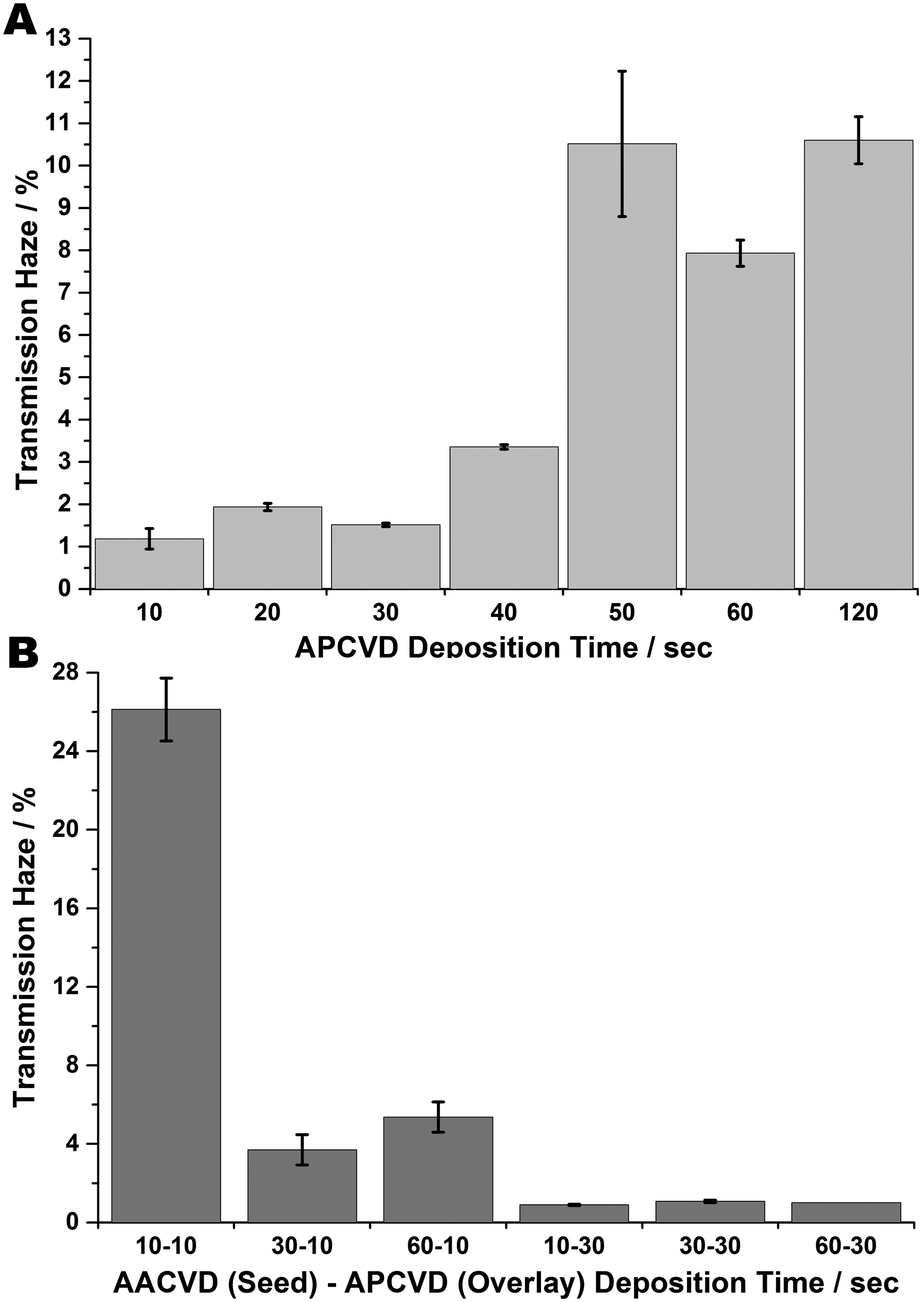 | ||
| Fig. 5 Transmission haze measurements of FTO films (A) formed at increasing deposition times via APCVD; (B) formed at various AACVD seed – APCVD overlay times. | ||
The seeming variance between increased roughness and low haze can be explained by the fact that any obtrusive feature contributes to the surface roughness whereas only angled surface features are able to scatter light and so contribute to increased haze. Efficient scattering of visible and near IR light requires that surface features be of the order of the wavelength range they are required to scatter; 400–1200 nm. The high roughness, low haze values obtained from these results indicate the high prevalence of flat or very low-angled obtrusions such that there is little overall scattering of light.76–79 Solely APCVD-produced films demonstrate increasing transmittance haze with deposition time. However, seeding seems to stabilise these haze values, such that there is little change with increasing APCVD overlay time; the values are lower and more stable throughout.
Calculated optical bandgap values correlate well with those calculated via the carrier concentration variation. All indicate a value greater than the recognised undoped, characteristic SnO2 value of 3.6 eV (see ESI† – S4), indicating a blue-shift of the low-wavelength absorption edge as explained by the Moss–Burstein effect.2 This is expected for degenerately doped FTO semiconductors and is caused by the presence of extrinsically generated charge carriers as effected by the F-dopant donor bands in the bandgap region localised near to the SnO2 conduction bands.2,73,80
3.4 Structural properties
XRD data (see Fig. 6) highlights the predominance of the cassiterite form of SnO2 deposited in all cases. Additionally, in many cases peaks not assignable to SnO2 are also observed. These have been attributed to the tetragonal litharge structure of the stannous oxide (SnO) phase, indicating that the seeding method induces a degree of disorder on the overgrown film resulting in the formation of kinetically stable oxide forms. The reason for this is thought partly due to the reaction chemistry during film formation; the greater degree of gas-phase decomposition prior to reaction and film formation on the surface meaning the species that co-ordinate to the surface have already undergone extensive decomposition and reaction, allowing SnO formation. However, because the experimental temperatures favour formation of SnO2, there is thought to be a conversion involving a two-step disproportionation reaction, possibly involving a Sn3O4 intermediate:7,81,82| 4SnO → Sn3O4 + β-Sn | (1) |
| Sn3O4 → SnO2 + 2β-Sn | (2) |
 | ||
| Fig. 6 XRD of FTO thin films formed at various APCVD deposition times or AACVD seed – APCVD overlay times (A–C) and reference experimental XRD patterns of SnO2 and SnO, both synthesised by AACVD (D). | ||
Although β-Sn was not identified in this instance, it has been in previous FTO syntheses.3 Whilst extended overlay times seem to steadily resolve this induced disorder as a result of seeding, nevertheless, peaks from the SnO form are still frequently observed. For example, the anomalous XRD peak at approximately 31° has been attributed to the SnO(101) peak. Further, whether seeding occurred defined whether growth tended towards the solely APCVD or AACVD characteristics, including preferred orientation and grain crystallite and grain size characteristics (see Fig. 6). The results indicate a decrease in crystallite size with both increased seeding and overlay times (see Table 1), with the smallest values obtained with a 30 second APCVD overlay deposition, tending towards values obtained solely through AACVD deposition methods. This is in line with observations from SEM and AFM images and reinforces the belief that these effects are due to the AA-AP CVD seed-overlay synthesis strategy rather than fluorine dopant incorporation.
Upon increased APCVD overlay times, there is a gradual change from favouring the (110) plane, which correlates to the most dense crystallographic direction and in other systems corresponds to the presence of FO−1 species, towards the (101) and (211) planes.83,84 The (211) direction in other deposition systems is thought to be characterised by low growth rates and is believed to be favoured during initial thin film formation.84–88
Raman data (see ESI† – S4) merely indicates increasing crystallinity and SnO2 density and thickness with increased deposition times, as indicated by more defined and intense Raman bands.89 No other impurities or tin–oxygen states are observed in the Raman spectrum, although bands attributable to oxygen vacancies, SnO2 disorder and nanocrystallite dimensions were also observed.90–93 However, due to the poor Raman scattering capabilities of SnO2, such bands were only observable at higher film thicknesses, corresponding to longer deposition times. Assuming compositional uniformity across the various AA-AP CVD seed-overlay depositions (as opposed to morphological and film thickness differences), it is thought such signals are applicable across all films produced here.
XPS results illustrate the presence of a single fluorine anion state at around 684.6 eV B.E. within the SnO2 films, corresponding to a substitutional incorporation (see Fig. 7A–C). Fluorine is present throughout the film at a reasonably uniform level, at ≈2.4% when looking solely at fluorine and tin presence. Its presence is also reinforced by EDS detection methods. This is unsurprising given the chemical consistency of precursors in the AACVD seeding layer and the APCVD overlay; the variation of deposition time is the main experimental variable. Thus, the differences seen between samples seems due to variations in seed-overlay times, with both longer seed and overlay periods giving a more homogeneous product. Further, the data reinforces the concept of doping as a flexible control over semiconductor conductivity. Dual Sn chemical environments were only identified at the surface of each of the analysed films, in line with XRD data; the bulk of the material seemed uniform and comprised tin as Sn4+ (see Fig. 7D).
 | ||
| Fig. 7 Illustrative F-1s XPS sputtered depth profile spectra representative of FTO films formed at various AACVD seed - APCVD overlay times (A), XPS calculated F-1s binding energy positions (B), fluorine dopant concentration (C) and illustrative Sn-3d surface scan (D). | ||
3.5 Electrical conductivity properties
Hall Effect probe measurements (see Table 1) indicate the presence of n-type semiconductors with large carrier concentrations (≈× 1020 cm−3), yielding highly conductive FTO thin films, as indicated by the generally low resistivity values of the order of ≈× 10−3 Ω cm. The phenomenon of high conductivity has long been attributed to the ability of F− to substitute O2− on the SnO2 lattice, acting as a single free electron donor (FO−1) and so yielding a higher electron carrier density overall.83,94–96 The high carrier concentration values correlate with the high and early-onset reflectance properties observed (see ESI† – S3), caused by the plasmon absorption edge blue-shifts in the IR region of transmittance spectra as well as the optical bandgap shifts. The electron carrier mobility values, spanning ≈1–20 cm2 V−1 s−1, are generally good for FTO films of this type, albeit being slightly lower than commercial standards. This could potentially be explained by the presence of SnO; the intrinsically p-type material retarding movement of charge carriers by acting as an electron trap/recombination centre and so reducing the overall mobility values.3,97 Film thickness relationships indicate there is a decrease in resistivity and carrier density with increasing thickness whilst carrier mobility increases. Generally, there is an increase in mobility and conductivity with both increasing seeding and overlayer depositions, but a decrease in carrier density in the FTO films.4 Conclusions
A novel seeding-overlay method utilising AACVD and APCVD techniques respectively, was identified as a means of directing the growth and effected morphology of highly transparent, conducting, polycrystalline fluorine-doped tin oxide thin films. This proprietary hybrid AA-AP CVD deposition system is a stable, controllable and reproducible synthesis method providing a direct means of growth and morphology control that allows films with excellent homogeneity to be obtained, all within an industrially compatible timeframe, making it amenable to large area deposition. The method allows for dense, highly adhesive films, with a more uniform, controllable microstructure to be synthesised as compared to conventional FTO thin films and current commercial synthesis methods. It could also potentially allow for less precursor to be used or high-quality products to be obtained at lower deposition temperatures in the longer term.A minimum required seeding time is necessary for the underlying layer to template structure evolution and to allow conformal coverage, which, in this study, is in the region of 30 seconds, followed by an APCVD overlay. AFM mapping and SEM imaging indicate improved texturing and increased surface roughness results from the use of seeding layers as well as low transmission haze values, ideal properties for low haze thin film front contacts as required in many optoelectronic applications, e.g.; smartphones. Other prospective uses include high-clarity, TCO and low emissivity applications as well as the variable microstructure which allows for greater scope in the design of multi-layer stacks, altering the way subsequent coatings contact the FTO layer. The seed-overlay method itself has great potential in terms of application to different systems and materials, the wider applications of which are currently the focus of further study. Thus, the work presented here has important implications in FTO synthesis, morphology manipulation and the attainment of high-performing TCM samples.
Acknowledgements
NN would like to thank the UK EPSRC for a Doctoral Prize, Dr Steve Hudziak of UCL Electronic and Electrical Engineering for help with AFM, Dr Tom Gregory and Mr Kevin Reeve for help with SEM, Dr Steve Firth for help with Raman measurements and Pilkington-NSG for float glass substrates and transmission haze measurements. CJC and IPP would like to thank the EPSRC for funding-grant EP/K001515.References
- D. S. Ginley and C. Bright, MRS Bull., 2000, 25, 15–18 CrossRef CAS.
- C. G. Granqvist, Sol. Energy Mater. Sol. Cells, 2007, 91, 1529–1598 CrossRef CAS PubMed.
- N. Noor and I. P. Parkin, J. Mater. Chem. C, 2013, 1, 984–996 RSC.
- N. Noor and I. P. Parkin, Thin Solid Films, 2013, 532, 26–30 CrossRef CAS PubMed.
- C. Chew, P. Bishop, C. Salcianu, C. J. Carmalt and I. P. Parkin, RSC Adv., 2014, 4, 13182–13190 RSC.
- C. K. T. Chew, C. Salcianu, P. Bishop, C. J. Carmalt and I. P. Parkin, J. Mater. Chem. C, 2015, 3, 1118–1125 RSC.
- M. Batzill and U. Diebold, Phys. Chem. Chem. Phys., 2007, 9, 2307–2318 RSC.
- J. T. Wang, X. L. Shi, W. W. Liu, X. H. Zhong, J. N. Wang, L. Pyrah, K. D. Sanderson, P. M. Ramsey, M. Hirata and K. Tsuri, Sci. Rep., 2014, 4, 1–9 Search PubMed.
- J. R. Bellingham, W. A. Phillips and C. J. Adkins, J. Mater. Sci. Lett., 1992, 11, 263–265 CrossRef CAS.
- H. Peelaers, E. Kioupakis and C. G. V. de Walle, Appl. Phys. Lett., 2012, 100, 011914 CrossRef PubMed.
- A. Kafizas, N. Noor, P. Carmichael, D. O. Scanlon, C. J. Carmalt and I. P. Parkin, Adv. Funct. Mater., 2014, 24, 1758–1771 CrossRef CAS PubMed.
- A. Kafizas, N. Noor, C. J. Carmalt and I. P. Parkin, J. Mater. Chem. C, 2013, 1, 6335–6346 RSC.
- S. Sathasivam, A. Kafizas, S. Ponja, N. Chadwick, D. S. Bhachu, S. M. Bawaked, A. Y. Obaid, S. Al-Thabaiti, S. N. Basahel, C. J. Carmalt and I. P. Parkin, Chem. Vap. Deposition, 2014, 20, 69–79 CrossRef CAS PubMed.
- D. S. Bhachu, S. Sathasivam, G. Sankar, D. O. Scanlon, G. Cibin, C. J. Carmalt, I. P. Parkin, G. W. Watson, S. M. Bawaked, A. Y. Obaid, S. Al-Thabaiti and S. N. Basahel, Adv. Funct. Mater., 2014, 24, 5075–5085 CrossRef CAS PubMed.
- S. M. Bawaked, S. Sathasivam, D. S. Bhachu, N. Chadwick, A. Y. Obaid, S. Al-Thabaiti, S. N. Basahel, C. J. Carmalt and I. P. Parkin, J. Mater. Chem. A, 2014, 2, 12849–12856 CAS.
- Y. Furubayashi, T. Hitosugi, Y. Yamamoto, K. Inaba, G. Kinoda, Y. Hirose, T. Shimada and T. Hasegawa, Appl. Phys. Lett., 2005, 86, L1063–L1065 CrossRef PubMed.
- T. Hitosugi, Y. Furubayashi, A. Ueda, K. Itabashi, K. Inaba, Y. Hirose, G. Kinoda, Y. Yamamoto, T. Shimada and T. Hasegawa, Jpn. J. Appl. Phys., 2005, 44, L1063 CrossRef CAS.
- C. Sotelo-Vazquez, N. Noor, A. Kafizas, R. Quesada-Cabrera, D. O. Scanlon, A. Taylor, J. R. Durrant and I. P. Parkin, Chem. Mater., 2015, 27, 3234–3242 CrossRef CAS.
- H.-R. Wenk and P. V. Houtte, Rep. Prog. Phys., 2004, 67, 1367 CrossRef CAS.
- K. Taira, Y. Hirose, S. Nakao, N. Yamada, T. Kogure, T. Shibata, T. Sasaki and T. Hasegawa, ACS Nano, 2014, 8, 6145–6150 CrossRef CAS PubMed.
- J. Muller, B. Rech, J. Springer and M. Vanecek, Sol. Energy, 2004, 77, 917–930 CrossRef PubMed.
- A. Taylor, I. Parkin, N. Noor, C. Tummeltshammer, M. S. Brown and I. Papakonstantinou, Opt. Express, 2013, 21, A750–A764 CrossRef PubMed.
- E. Yablonovitch and G. Cody, IEEE Trans. Electron Devices, 1982, 29, 300–305 CrossRef.
- A. M. Sukhadia, D. C. Rohlfing, M. B. Johnson and G. L. Wilkes, J. Appl. Polym. Sci., 2002, 85, 2396–2411 CrossRef CAS PubMed.
- H. Byker, F. Bauer and W. Tonar, Electro-optic device including a low sheet resistance, high transmission transparent electrode, US Pat., 5,923,457, 1999 Search PubMed.
- R. Baetens, B. P. Jelle and A. Gustavsen, Sol. Energy Mater. Sol. Cells, 2010, 94, 87–105 CrossRef CAS PubMed.
- B. Petter Jelle, Sol. Energy Mater. Sol. Cells, 2012, 96, 1–28 CrossRef PubMed.
- P. F. Gerhardinger and R. J. Mccurdy, MRS Proceedings: Symposium J Thin Films for Photovoltaic and Related Device, 1996.
- M. D. Allendorf, J. Sopko, W. G. Houf, Y. K. Chae, A. H. McDaniel, M. Li and J. McCamy, On-line coating of glass with tin oxide by atmospheric pressure chemical vapor deposition, 2006 Search PubMed.
- T. D. Manning, I. P. Parkin, M. E. Pemble, D. Sheel and D. Vernardou, Chem. Mater., 2004, 16, 744–749 CrossRef CAS.
- S. D. Ponja, S. Sathasivam, I. P. Parkin and C. J. Carmalt, RSC Adv., 2014, 4, 49723–49728 RSC.
- N. Chadwick, S. Sathasivam, A. Kafizas, S. M. Bawaked, A. Y. Obaid, S. Al-Thabaiti, S. N. Basahel, I. P. Parkin and C. J. Carmalt, J. Mater. Chem. A, 2014, 2, 5108–5116 CAS.
- D. S. Bhachu, M. R. Waugh, K. Zeissler, W. R. Branford and I. P. Parkin, Chem. – Eur. J., 2011, 17, 11613–11621 CrossRef CAS PubMed.
- S. Chen, N. Noor, I. P. Parkin and R. Binions, J. Mater. Chem. A, 2014, 2, 17174–17182 CAS.
- G. Walters and I. Parkin, Appl. Surf. Sci., 2009, 255, 6555–6560 CrossRef CAS PubMed.
- M. S. Hill, A. L. Johnson, T. D. Manning, K. C. Molloy and B. J. Wickham, Inorg. Chim. Acta, 2014, 422, 47–56 CrossRef CAS PubMed.
- N. P. Chadwick, S. Sathasivam, S. M. Bawaked, M. Mokhtar, S. A. Althabaiti, S. N. Basahel, I. P. Parkin and C. J. Carmalt, J. Mater. Chem. A, 2015, 3, 4811–4819 CAS.
- P. Marchand, I. A. Hassan, I. P. Parkin and C. J. Carmalt, Dalton Trans., 2013, 42, 9406–9422 RSC.
- T. Manning, I. Parkin and M. Waugh, Method for coating substrates, WO Pat., PCT/GB2012/050,844, 2012 Search PubMed.
- M. R. Waugh, PhD thesis, University College London (UCL), 2011.
- V. Diesen, M. Jonsson and I. P. Parkin, Chem. Vap. Deposition, 2013, 19, 355–362 CrossRef CAS PubMed.
- X. Ling, Y.-H. Lee, Y. Lin, W. Fang, L. Yu, M. S. Dresselhaus and J. Kong, Nano Lett., 2014, 14, 464–472 CrossRef CAS PubMed.
- B. Lecohier, B. Calpini, J. Philippoz and H. van den Bergh, J. Appl. Phys., 1992, 72, 2022–2026 CrossRef CAS PubMed.
- J. Heath, S. Gates and C. Chess, Appl. Phys. Lett., 1994, 64, 3569–3571 CrossRef CAS PubMed.
- S. Nicolay, M. Benkhaira, L. Ding, J. Escarre, G. Bugnon, F. Meillaud and C. Ballif, Sol. Energy Mater. Sol. Cells, 2012, 105, 46–52 CrossRef CAS PubMed.
- K. Kang, S.-K. Kim, C.-J. Kim and M.-H. Jo, Nano Lett., 2008, 8, 431–436 CrossRef CAS PubMed.
- A. Masood, M. Aslam, M. A. Tamor and T. J. Potter, J. Electrochem. Soc., 1991, 138, L67–L68 CrossRef CAS PubMed.
- G. Chen, S. Chen and Y. Lu, Electrochem. Commun., 2010, 12, 1483–1486 CrossRef CAS PubMed.
- R. W. Fiordalice, R. I. Hegde and H. Kawasaki, J. Electrochem. Soc., 1996, 143, 2059–2063 CrossRef CAS PubMed.
- D. Calestani, S. C. Dhanabalan, M. Villani, L. Lazzarini and A. Zappettini, CrystEngComm, 2014, 16, 1696–1701 RSC.
- V.-A. Antohe, M. Mickan, F. Henry, R. Delamare, L. Gence and L. Piraux, Appl. Surf. Sci., 2014, 313, 607–614 CrossRef CAS PubMed.
- A. R. Rathmell, S. M. Bergin, Y.-L. Hua, Z.-Y. Li and B. J. Wiley, Adv. Mater., 2010, 22, 3558–3563 CrossRef CAS PubMed.
- H. Wang, Y. Bai, Q. Wu, W. Zhou, H. Zhang, J. Li and L. Guo, Phys. Chem. Chem. Phys., 2011, 13, 7008–7013 RSC.
- S.-Y. Chang, N.-H. Yang and Y.-C. Huang, J. Electrochem. Soc., 2009, 156, K200–K204 CrossRef CAS PubMed.
- J. Ding, Y. Liu, C. Tan and N. Yuan, Nanoscale Res. Lett., 2012, 7, 368 CrossRef PubMed.
- S. Hiboux and P. Muralt, J. Eur. Ceram. Soc., 2004, 24, 1593–1596 CrossRef CAS.
- B. Toby, J. Appl. Crystallogr., 2001, 34, 210–213 CrossRef CAS.
- A. Larson and R. V. Dreele, General Structure Analysis System (GSAS), Los Alamos National Laboratory Report LAUR 86-748, 1994, pp. 86–748 Search PubMed.
- D. Neas and P. Klapetek, Cent. Eur. J. Phys., 2012, 10, 181–188 Search PubMed.
- J. M. Schneider, PhD thesis, Technischen Universitt Berlin, 2006.
- D. J. Safarik and C. B. Mullins, J. Chem. Phys., 2003, 119, 12510–12524 CrossRef CAS PubMed.
- S. Armini and P. M. Vereecken, ECS Trans., 2010, 25, 185–194 CAS.
- S. Armini, J. Electrochem. Soc., 2011, 158, D390–D394 CrossRef CAS PubMed.
- S. Armini, Z. Tokei, H. Volders, Z. El-Mekki, A. Radisic, G. Beyer, W. Ruythooren and P. M. Vereecken, Microelectron. Eng., 2011, 88, 754–759 CrossRef CAS PubMed.
- M. J. Willey and A. C. West, Electrochim. Acta, 2007, 52, 6484–6489 CrossRef CAS PubMed.
- J. Roth, Industrial Plasma Engineering: Volume 2 - Applications to Nonthermal Plasma Processing, Taylor & Francis, 2001 Search PubMed.
- D. W. Butler, C. T. H. Stoddart and P. R. Stuart, J. Phys. D: Appl. Phys., 1970, 3, 877 Search PubMed.
- D. I. Fotiadis and K. F. Jensen, J. Cryst. Growth, 1990, 102, 743–761 CrossRef CAS.
- S. Abbasi, S. Kitayaporn, D. T. Schwartz and K. F. Bhringer, Nanotechnology, 2011, 22, 165303 CrossRef PubMed.
- H. M. Yates, P. Evans, D. W. Sheel, S. Nicolay, L. Ding and C. Ballif, Surf. Coat. Technol., 2012, 213, 167–174 CrossRef CAS PubMed.
- L. Cuiping, D. Wei, Q. Lirong, L. Mingji, S. Dazhi, G. Chengyao and Y. Baohe, Diamond Relat. Mater., 2014, 49, 48–54 CrossRef PubMed.
- T. A. N. Peiris, H. Alessa, J. S. Sagu, I. A. Bhatti, P. Isherwood and K. G. U. Wijayantha, J. Nanopart. Res., 2013, 15, 458–484 Search PubMed.
- H. Liu, V. Avrutin, N. Izyumskaya, U. Ozgur and H. Morko, Superlattices Microstruct., 2010, 48, 458–484 CrossRef CAS PubMed.
- P. P. Edwards, A. Porch, M. O. Jones, D. V. Morgan and R. M. Perks, Dalton Trans., 2004, 2995–3002 RSC.
- G. J. Exarhos and X.-D. Zhou, Thin Solid Films, 2007, 515, 7025–7052 CrossRef CAS PubMed.
- Y. Yin, N. Sahraei, S. Venkataraj, S. Calnan, S. Ring, B. Stannowski, R. Schlatmann, A. G. Aberle and R. Stangl, Int. J. Photoenergy, 2014, 1–8 Search PubMed.
- N. Sahraei, K. Forberich, S. Venkataraj, A. G. Aberle and M. Peters, Opt. Express, 2014, 22, A53–A67 CrossRef CAS PubMed.
- I. Simonsen, A. Larsen, E. Andreassen, E. Ommundsen and K. Nord-Varhaug, Phys. Rev. A: At., Mol., Opt. Phys., 2009, 79, 063813 CrossRef.
- N. Sahraei, S. Venkataraj, A. G. Aberle and M. Peters, Proc. SPIE, 2014, 8981, 89811D CrossRef PubMed.
- S. J. Ikhmayies and R. N. Ahmad-Bitar, Renewable Energy, 2013, 49, 143–146 CrossRef CAS PubMed.
- W. Choi, H. Sung, K. Kim, J. Cho, S. Choi, H.-J. Jung, S. Koh, C. Lee and K. Jeong, J. Mater. Sci. Lett., 1997, 16, 1551–1554 CrossRef CAS.
- O. M. Berengue, R. A. Simon, A. J. Chiquito, C. J. Dalmaschio, E. R. Leite, H. A. Guerreiro and F. E. G. Guimares, J. Appl. Phys., 2010, 3, 033717 CrossRef PubMed.
- C. D. Canestraro, M. M. Oliveira, R. Valaski, M. V. da Silva, D. G. David, I. Pepe, A. F. da Silva, L. S. Roman and C. Persson, Appl. Surf. Sci., 2008, 255, 1874–1879 CrossRef CAS PubMed.
- D. Bélanger, J. P. Dodelet, B. A. Lombos and J. I. Dickson, J. Electrochem. Soc., 1985, 132, 1398–1405 CrossRef PubMed.
- J. Jeong, S. P. Choi and K. J. Hong, J. Korean Phys. Soc., 2006, 48, 960–963 CAS.
- C. Agashe and S. S. Major, J. Mater. Sci., 1996, 31, 2965–2969 CrossRef CAS.
- C. Agashe, J. Hpkes, G. Schpe and M. Berginski, Sol. Energy Mater. Sol. Cells, 2009, 93, 1256–1262 CrossRef CAS PubMed.
- C. Agashe, B. Marathe, M. Takwale and V. Bhide, Thin Solid Films, 1988, 164, 261–264 CrossRef.
- M. Batzill, Sensors, 2006, 6, 1345–1366 CrossRef CAS PubMed.
- T. T. Van Tran, T. Si Bui, S. Turrell, B. Capoen, P. Roussel, M. Bouazaoui, M. Ferrari, O. Cristini and C. Kinowski, J. Raman Spectrosc., 2011, 43, 869–875 CrossRef PubMed.
- K. McGuire, Z. W. Pan, Z. L. Wang, D. Milkie, J. Menndez and A. M. Rao, J. Nanosci. Nanotechnol., 2002, 2, 499–502 CrossRef CAS PubMed.
- T. Lan, C. W. Li and B. Fultz, Phys. Rev. B: Condens. Matter Mater. Phys., 2012, 86, 134302 CrossRef.
- A. Diguez, A. Romano-Rodrguez, A. Vil and J. R. Morante, J. Appl. Physiol., 2001, 90, 1550–1557 CrossRef PubMed.
- L. Chinnappa, K. Ravichandran, K. Saravanakumar, G. Muruganantham and B. Sakthivel, J. Mater. Sci.: Mater. Electron., 2011, 22, 1827–1834 CrossRef CAS.
- F. E. Akkad and S. Joseph, J. Appl. Phys., 2012, 112, year CrossRef PubMed.
- D. Cheng, M. Zhang, J. Chen, C. Yang, X. Zeng and D. Cao, J. Phys. Chem. C, 2014, 118, 2037–2043 CAS.
- L. Y. Liang, Z. M. Liu, H. T. Cao and X. Q. Pan, ACS Appl. Mater. Interfaces, 2010, 2, 1060–1065 CAS.
Footnote |
| † Electronic supplementary information (ESI) available. See DOI: 10.1039/c5tc02144h |
| This journal is © The Royal Society of Chemistry 2015 |