
 Open Access Article
 This Open Access Article is licensed under a
 Creative Commons Attribution 3.0 Unported Licence
Synthesis and fluorescence properties of a nanoisland-structured SiOx/CuxO composite†
Xu
Lu
,
Yohei
Ishida
,
Mai Thanh
Nguyen
and
Tetsu
Yonezawa
*
Division of Materials Science and Engineering, Faculty of Engineering, Hokkaido University, Kita 13 Nishi 8, Sapporo, Hokkaido, 060-8628 Japan. E-mail: tetsu@eng.hokudai.ac.jp
First published on 7th July 2015
Abstract
A nanoisland-structured SiOx (x ≤ 2)/CuxO (x ≤ 2) composite was prepared from a Cu-deposited Si wafer by electrochemical anodization in a hydrofluoric acid (HF) and ferric nitrate (Fe(NO3)3) electrolyte. The surface of the nanoisland comprised Cu, Cu oxides, Si nanoparticles and Si oxides. The distribution of elemental Cu on the surface was uniform. Cracks and native Cu-oxides in the deposited Cu layer are the two main factors for the formation of the nanoisland-structured surface. Different from the single red photoluminescence (PL) band emitted from the electrochemical anodized bare Si wafer, a dual-visible PL band with comparable intensities at red and blue ranges was observed. The red PL quenching did not occur in this Cu-ion-doped nanostructured Si due to the different distribution areas of Cu+ and the red PL centre. The red PL originates due to oxygen defects in the band gap of Si nanoparticles/Si oxides; the blue PL is the consequence of the band-to-band transitions between 3d10 and 3d94s1 of Cu+ ions and the intra d → d band transition of Cu2+ ions in the interstitial vacancies of Si oxides. Compared with the electrochemical anodized bare Si sample with a single PL band, the nanoisland-structured SiOx/CuxO composite emitting a dual-PL-band is more promising for fabricating white light emitters.
1. Introduction
Nanostructured silicon (Si) and related research studies have become hot topics in recent times. As the size of the Si particles reduces to less than 5 nm, some native properties such as the band gap, and thermal and optical properties become drastically different from those of larger-sized Si. Phenomena such as fluorescence, surface plasmon resonance and surface-enhanced Raman scattering are available for Si-related materials1–4 that extend the application areas of Si, especially Si-based optoelectronics. In general, the most common preparation method of nanostructured Si is electrochemical anodization in HF-containing organic solutions.1 In this method, the obtained samples always show a porous morphology with a single visible photoluminescence (PL) band in the red region.5,6 Therefore, to be used as a multi-visible-band emitting material such as a white light source, nanostructured Si should be in a combination with other fluorescence materials.7Metal and metal oxides combined with nanostructured Si are an efficient method to enhance the performances of nanostructured Si composites.8,9 Various efforts have been devoted to research the combination of noble metals or noble metal oxides with nanostructured Si.10,12 In comparison with other noble metals, copper (Cu) is a commonly used metal with a lower electrical resistivity, lower cost, higher diamagnetism and electro-migration resistivity. Therefore, fabricating Cu and Cu-oxides/nanostructured Si composites has attracted much attention. Photocatalytic H2 evolution capacity can also be enhanced by a nanocrystalline Cu2O/Si nanowire core–shell composite.13 The contact of p-type Cu oxides and n-type Si formed a heterojunction structure for applying to a photodiode.14 While investigating the optical properties of Cu/Cu oxides/porous Si composites, various Cu-coated aged porous Si showed intensive blue emission, while the native red PL from porous Si was quenched.15 Naddaf et al. has reported that the PL emission from porous Si (PSi) could be modified by the formation of CuO/PSi composites.11 An additional weak blue PL peak besides the common red emission was detected in their sample; however, the intensity of the blue emission is not comparable to that of the red emission. The existence of blue emission from the CuO/porous Si composite is promising for research on the full-range PL emission of Si/Cu composites. Therefore, there is a demand for obtaining more intensive blue emission for dual/multiple band PL emitted by Si/Cu based composites.
So far, although nano Cu/Cu+ can show blue emission,16 Cu/nanostructured Si composites usually show either a single blue PL17 as the presence of Cu+ or Cu2+ disrupts the native red PL from nanostructured Si, or a single red PL due to the relatively weak blue PL centres. It is necessary to design Cu–Cu oxide/Si composites with a suitable structure to obtain the dual/multiple-band PL emission with intensive intensity. One approach is making the distribution of the Cu+/Cu2+ and the red PL centres associated with Si/non-stoichiometric Si oxide nanoparticles well separated to avoid the mutual disturbance between them. For the fabrication of such structures, in this study, we synthesized a nanoisland-structured SiOx/CuxO composite via a two-step process. In the first step, a thin Cu film was deposited on a Si substrate by magnetron sputtering; and in the second step, the Cu deposited Si wafer was electrochemically corroded in an aqueous electrolyte solution of HF and Fe(NO3)3. The thus-prepared sample showed a nanoisland surface morphology instead of the traditional porous one. Simultaneously, a dual-visible PL band was observed in the red and blue regions with comparable intensities. Introducing Cu-related defects on the surface resulted in the blue PL emission and its enhancement. In contrast to previous results,18 the red PL quenching in Cu-ion-doped nanostructured Si did not occur due to the different distribution areas of the Cu+/Cu2+ and the red PL centres on the surface of the prepared sample. Compared to traditional nanostructured Si that emits a single fluorescence band, the dual-band PL with comparable intensities from our sample is more promising for fabricating white-light-emitting devices.
2. Experimental methods
2.1 Preparation of the nanoisland-structured SiOx/CuxO composite
First, Cu thin film was deposited onto a Si wafer by using a magnetron sputtering method as follows. The phosphorus-doped, 〈111〉-oriented Si wafer (Nilaco, Japan), with an electrical resistivity less than 0.02 Ω cm, was washed with ethanol and acetone by ultrasonic oscillation for 5 min, and then it was rinsed again with purified water. The pressure of the sputtering vacuum chamber was less than 5.0 × 10⁻³ Pa and then Ar gas was purged into the chamber at 2 Pa. The distance between the sample and the sputtering target was maintained at 60 mm. The sputtering current and period were set to 30 mA and 3 min, respectively. The thickness of the deposited Cu layer is estimated to be ∼10 nm. Then, the obtained SiCu sample was anodized in an electrolyte consisting of Fe(NO3)3 (0.008 mol dm−3, Junsei, Japan), HF solution (46%, Stella Chemifa, Japan), and purified water (volume ratio, HF solution![[thin space (1/6-em)]](https://www.rsc.org/images/entities/char_2009.gif) :H2O = 7:5 (v/v)) with a current density of 100 mA cm−2 for 1 h. The obtained sample was washed with purified water and dried in air at room temperature.
:H2O = 7:5 (v/v)) with a current density of 100 mA cm−2 for 1 h. The obtained sample was washed with purified water and dried in air at room temperature.
2.2 Characterization
The surface structure was observed using a JEOL JSM-6510LA scanning electron microscope (SEM), and surface composition analysis was carried out using a JEOL JPS-9200 X-ray photoelectron spectroscopy (XPS) device equipped with a monochromatic Mg Kα source operating at 100 W under ultrahigh vacuum (∼1.0 × 10⁻⁷ Pa) conditions; the obtained spectra were calibrated by the C 1s peak. Photoluminescence spectra were captured using a Jasco FP-6600 spectrofluorometer. A JEOL JIB-4600F/HDK multibeam system was used to process the FIB sample to obtain a final thickness less than 100 nm and the thus-prepared FIB sample was transferred to a molybdenum-grid transmission electron microscope (TEM) stage. The lateral structure, the related electron diffraction patterns and the energy-dispersive spectroscopy (EDS) spectra of the prepared sample were obtained using a JEM-2010 transmission electron microscope (TEM, 200 kV).3. Results and discussion
3.1 Morphology, structure and composition of the nanoisland-structured SiOx/CuxO composite
The surface morphology of the as-prepared SiOx/CuxO composite is shown in Fig. 1b. The isolated nanoisland is observed on the surface with a diameter of 200–500 nm. Compared with the surface of the anodized bare Si sample shown in Fig. 1a, the density of the nanoisland decreased and the distance among nanoislands increased. Moreover, the HR-TEM image (Fig. 1c) shows the Si nanoparticles on the surface and the lattice fringes with a distance of 3.15 Å, corresponding to distorted Si(111) (3.13 Å). These Si nanoparticles play an important role in changing the native properties due to the quantum confinement (QC).1,9 | ||
| Fig. 1 (a) Scanning electron microscopy (SEM) image of the electrochemically anodized bare Si. (b) SEM image of the surface morphology of the anodized SiOx/CuxO composite. (c) High-resolution transmission electron microscopy (HR-TEM) image of the surface structure of the sample shown in (b), a measured interplanar distance of 3.15 Å corresponds to the Si(111) plane (3.13 Å). | ||
Surface composition analysis of the prepared sample was carried out by XPS as shown in Fig. 2. The wide-scan XPS spectrum shown in Fig. 2a indicates that the sample surface comprised Si, Cu, C and O (H cannot be detected by XPS, even though it may exist on the surface). Detailed narrow-scan XPS spectra of Si 2p and Cu 2p3/2 are shown in Fig. 2b and c. In the Si 2p spectrum, the main peak can be deconvoluted into five peaks at 100.8, 101.7, 102.5, 103.1 and 104.9 eV, which corresponded to Si–O–Cu, SiO, SiOx (1 < x < 2), SiO2 and Si–F structures (in the order of increasing electro-negativity values of the elements bonded to Si from Cu–O–, to O and F). F was not appeared in the wide-scan XPS spectrum, however, narrow-scan XPS can show a weak F 1s peak (see Fig. S1, ESI†). Concurrently, the narrow-scan XPS spectrum of Cu 2p3/2 showed that the Si–O–Cu structure also presented in the spectrum of the Cu 2p3/2 area as well as cuprous oxide and cupric oxide. The Cu ions are driven by electric potential and are moved into the protuberant nanoisland; these Cu ions may fill the interstitial vacancies (SiO and SiOx) to form crystalline Cu and Cu-related defects (Si–O–Cu) that lead to blue PL. There was no characteristic peak of Si in the narrow-scan XPS spectra because the effective detection depth (less than 10 nm) of the XPS cannot reach the Si region, i.e., after anodization, the Si substrate was covered by Cu-oxides, Cu and Si-oxides, which will be discussed in Fig. 3.
 | ||
| Fig. 2 (a) XPS wide-scan spectrum of the freshly prepared nanoisland SiOx/CuxO composite. (b) and (c) XPS narrow scan spectra of the Si 2p area and the Cu 2p3/2 area of the freshly prepared nanoisland SiOx/CuxO composite, respectively. | ||
 | ||
| Fig. 3 (a) TEM image of the lateral structure of the prepared SiOx/CuxO composite (the sample was prepared by focused ion beam (FIB) treatment; the thickness was less than 100 nm after FIB treatment). (b)–(d) Electron diffraction patterns of the corresponding circular regions. | ||
The lateral morphology of the as-prepared nanoisland SiOx/CuxO composite is shown in Fig. 3a. The height of the obtained nanoisland composite was ∼150 nm. Simultaneously, different regions from the surface towards the Si substrate of the nanoisland composite were characterized by electron diffraction as shown in Fig. 3b–d. Diffraction patterns of the protuberant area (80 nm from the substrate, Fig. 3b) showed only crystalline Cu2O and Cu. The substrate is single-crystalline Si (Fig. 3c) and the sputtered Cu layer is only ∼10 nm in thickness. The composition of the protuberant area was determined to be crystalline Cu2O, Cu, amorphous Si oxides and amorphous CuO (as detected by XPS spectra shown in Fig. 2c). In the junction region (Fig. 3d) of the protuberant area and the bulk Si substrate, the pattern of Si was detected, although it was very weak. This indicated that Si nanoparticles shown in Fig. 1c may have come from this junction region and this explained the absence of Si in the XPS spectra shown in Fig. 2b. This result further indicates that the Si nanoparticle area and Cu-oxide-concentrated area are separated. As the Fe(NO3)3 is an oxidant, compared to the sample prepared in the commonly used HF/ethanol electrolyte, the post-anodization oxidation degree of the outermost surface of our sample should be higher. In other words, the outermost surface is mainly composed of Si oxides, and Si nanoparticles are not concentrated in this region. However, from the TEM image and diffraction results, it is found that Cu+/Cu2+ is mainly distributed at the outermost surface, indicating that red PL disturbance from Cu+/Cu2+ can be avoided, which is crucial for dual PL emission.
3.2 Formation mechanism of the nanoisland-structured SiOx/CuxO composite
The schematic of the formation of the nanoisland-structured SiOx/CuxO composite is shown in Fig. 4. Since the Cu cannot dissolve in HF, the key factors for the formation mechanism of the nanoisland-structured SiOx/CuxO composite are the native Cu oxides and the cracks in the Cu layer. As the Si surface is not an ideal surface, when a thin layer of Cu is deposited on the surface for a short period of time, it cannot form a continuous film due to surface tension (in our case, the thickness of the sputtered Cu layer was estimated to be ∼10 nm).19 That means the thin layer of Cu on the surface exists in the isolated block fashion (see Fig. S2, ESI†). After Cu was sputtered on the Si surface, a thin original oxide layer will be formed automatically. This Cu oxide is soluble in acid solutions. At the beginning of the corrosion, the Cu oxides were first dissolved by HF, and then, there are two corrosion routes.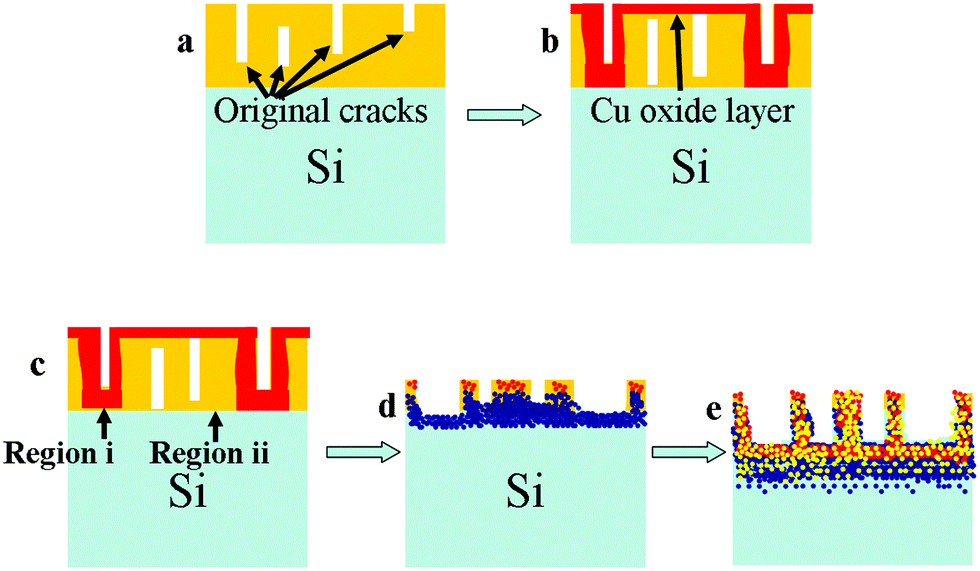 | ||
| Fig. 4 Schematic of the formation mechanism (red: Cu oxides; light blue: Si; dark blue dots: Si oxides; yellow: Cu). (a) Cu sputtered Si wafer; (b) Cu sputtered Si wafer in air; (c) start of anodization; (d) intermediate corrosion; (e) final obtained sample. | ||
Region i: this is the region underneath the bottom of the deep cracks. After the original Cu oxides were dissolved, these areas may come in contact with the electrolyte. Hence, the Si in this area may be corroded by the HF-containing electrolyte, as expressed in the below equations;
| Cu2O + 2HF → 2CuF + H2O | (1) |
| Si + 4HF + 4h+ → SiF4 + 4H+ | (2) |
Region ii: this is the region underneath the Cu layer or the shallow, inner cracks. In these regions, after the original Cu oxides were dissolved, the Cu layer still remains thick enough, so that the corrosion speed became very slow. With the help of the electric current, the Cu and the hydroxyl anion (OH−) formed Cu2O again, and then the corrosion is repeated as shown in eqn (1)–(3). This process is expressed as the following equations.
| 2Cu + 2OH− → Cu2O + H2O + 2e− | (3) |
| Cu2O + 2HF → 2CuF + H2O | (4) |
Finally, as the corrosion speeds of these two regions are different, the Cu-coated region became an island-shaped protuberance. In this case, the thickness of the Cu layer is a vital parameter for the formation of the surface morphology as the cracks and native oxide layer conditions have a close relationship with the thickness of the deposited Cu layer. More surface morphologies of the anodized Cu deposited Si wafer samples with different Cu thicknesses are shown in Fig S3 (ESI†).
3.3 Photoluminescence properties of the nanoisland-structured SiOx/CuxO composite
The fluorescence spectra of the freshly prepared nanoisland-structured SiOx/CuxO composite and the anodized bare Si are shown in Fig. 5a. Compared to the anodized bare Si, the nanoisland SiOx/CuxO composite showed two comparable PL bands at the red zone (peak centroid at 655 nm) and the blue zone (peak centroid at 469 nm). Compared to the reported Cu/nanostructured Si that has a single blue emission,17,18 the quenching of the red PL usually associated with the Cu ion doping did not occur;18 in comparison with Cu/nanostructured Si that has a single red emission,11 the intensity of the blue emission was comparable with that of the red one. For the red PL from anodized bare Si, the mechanism involves the oxygen defects that are in the QC (arising from the Si nanoparticles).20 In the case of the nanoisland SiOx/CuxO composite, the red PL still arose from the oxygen defects under the QC effect. The XPS spectrum (Fig. 2b) and the HR-TEM (Fig. 1c) image confirmed the presence of oxygen defects (SiO and Si3O4) and Si nanoparticles (nanosize induces the QC effect1). One phenomenon that usually occurs in Cu-ion-doped nanostructured Si is PL quenching because of the disruption of band-to-band transition due to the presence of Cu+/Cu2+ impurities in the band gap.18 However, in our case, it did not happen. From Fig. 3b and d, the Cu+ and Cu2+ are mainly distributed in the protuberant area while the red PL originated from the junction zone. The distribution of Cu oxides away from oxygen defects from Si oxides prevented quenching of the red PL. Concurrently, the full-width at half-maximum (FWHM) of the red PL peak became wider due to the diffusion of Cu ions into the Si substrate driven by electric potential and these ions were reduced to Cu (unlike Cu+ and Cu2+, pure Cu did not influence the native PL from nanostructured Si). So, the holes from the Cu ions may transport to the Si substrate to form more defects, broadening the PL peak in the red zone. Note that there was a small sub-band at 570 nm in the spectrum of the nanoisland SiOx/CuxO composite. This peak may be originated from the remaining Cu2O as the band gap energy of Cu2O is ∼2.1 eV (590 nm).21 In previous studies,11,17 the blue peak was attributed to carbonyl compounds; however, in our case, the aqueous electrolyte solution of HF/Fe(NO3)3 did not contain any organic molecules. That means carbonyl compounds are not the reason for blue PL. In our case, the blue peak originated from the Cu-related defects which play the same role as the luminescence centres.22–27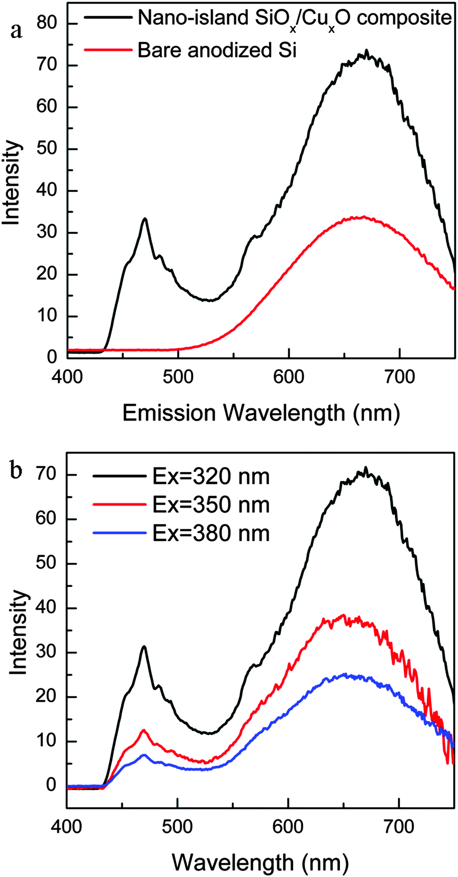 | ||
| Fig. 5 (a) The fluorescence spectra of the freshly prepared nanoisland SiOx/CuxO composite and anodized bare Si (the anodized bare Si was prepared by the same method without Cu coating before electrochemical anodization. The emission spectra were collected at an excitation wavelength of 320 nm). (b) The fluorescence emission spectra of the freshly prepared nanoisland SiOx/CuxO composite collected under different excitation wavelengths. | ||
As the Cu has a high diffusivity28 and Cu ions can be driven by electric potential, both Cu and Cu ions can diffuse into the protuberance layer. They will fill the interstitial vacancies and some of them may combine with the unstable SiO,29 resulting in the formation of Cu–SiOx (Fig. 2b and c, Si–O–Cu).15 All these defect states are PL centres. e.g., Cu-related defects in the band gap of SiOx that arose from 3d10 ↔ 3d94s1 transitions of Cu+ resulted in the blue emission.15,23,24 The spikes in the blue peak are due to the intra d → d band transition of Cu2+. In comparison with a previous report,11 the relatively enhanced blue emission may be due to the uniform distribution of Cu on the surface. Previously reported samples showed a fibre columnar structure and the Cu elements were only concentrated at the top of the fibre columns, so, the blue PL centres were only present there. However, in our samples, Cu distribution was very uniform (see Table S1, ESI†) on the surface, therefore, Cu defects can cover the entire surface area. The improved blue PL was the consequence of the increase in number of PL centres. From the spectra shown in Fig. 5b, under different excitation wavelengths, the two emission peaks appeared at identical positions and both these two peaks weakened in intensity as the excitation wavelength increased. This further confirmed that defects are the main reason for the visible fluorescence because of the constant value difference between the two defect levels.
4. Conclusions
In this study, a nanoisland-structured SiOx/CuxO composite was synthesized by electrochemical anodization. The nanoisland surface consisted of Si oxides, crystalline Cu and Cu2O, and amorphous CuO and Si nanoparticles. The formation mechanism of this nanoisland structure depended on the structure and oxidation of the sputtered Cu layer. The fluorescence spectrum of the freshly prepared nanoisland-structured SiOx/CuxO composite showed two luminescence bands at red and blue zones and the intensities of these two bands are comparable. The obtained results came from the designed structure which allows well separated distribution between the red and blue PL centres in the SiOx/CuxO composite. Compared to the single-PL-band sample, the dual-band one offers a promising approach for fabricating white light emitters.Acknowledgements
This work was partially supported by a Grant from Hokkaido University (to TY) and by a Grant-in-Aid for Scientific Research (A) (24241041, to TY). A part of this work was supported by the Nanotechnology Platform Program (Characterization and Fabrication, Hokkaido University) of the MEXT, Japan.Notes and references
- A. G. Cullis and L. T. Canham, Nature, 1991, 353, 335 CrossRef CAS PubMed.
- L. Gan, L. Sun, H. He and Z. Ye, J. Mater. Chem. C, 2014, 2, 2668 RSC.
- L. Tsakalakos, J. Balch, J. Fronheiser and B. A. Korevaar, Appl. Phys. Lett., 2007, 91, 233117 CrossRef PubMed.
- H. F. Wilson, L. McKenzie-Sell and A. S. Barnard, J. Mater. Chem. C, 2014, 2, 9451 RSC.
- T. Yanagishita, M. Imaizumi, K. Nishio and H. Masuda, ECS Solid State Lett., 2013, 2, P117 CrossRef CAS PubMed.
- H. Foll, M. Christophersen, J. Carstensen and G. Hasse, Mater. Sci. Eng., R, 2002, 39, 141 CrossRef.
- E. Kayahan, J. Lumin., 2010, 130, 1295 CrossRef CAS PubMed.
- Y. Fu, R. Yao and C. Cao, J. Mater. Chem. C, 2013, 1, 6422 RSC.
- L. Lin, X. Sun, R. Tao, J. Feng and Z. Zhang, Nanotechnology, 2011, 22, 075203 CrossRef PubMed.
- P. N. Vinod, RSC Adv., 2013, 3, 3618 RSC.
- M. Naddaf, O. Mrad and A. Al-zier, Appl. Phys. A: Mater. Sci. Process., 2014, 115, 1345 CrossRef CAS.
- O. A. Yeshchenko, I. M. Dmitruk, A. A. Alexeenko, M. Y. Losytskyy, A. V. Kotko and A. O. Pinchuk, Phys. Rev. B: Condens. Matter Mater. Phys., 2009, 79, 235438 CrossRef.
- Z. Xiong, M. Zheng, S. Liu, L. Ma and W. Shen, Nanotechnology, 2013, 24, 265402 CrossRef PubMed.
- R. A. Ismail, J. Semicond. Tech. Sci., 2009, 9, 51 CrossRef.
- X. Lu, Y. Ishida and T. Yonezawa, New J. Chem., 2015 10.1039/C5NJ00909J.
- M. Chiba, M. N. Thanh, Y. Hasegawa, Y. Obora, H. Kawasaki and T. Yonezawa, J. Mater. Chem. C, 2015, 3, 514 RSC.
- K. Y. Suh, Y. S. Kim and H. H. Lee, J. Appl. Phys., 2002, 91, 10206 CrossRef CAS PubMed.
- D. Andsager, J. Hilliard, J. M. Hetrick, L. H. AbuHassan, M. Plisch and M. H. Nayfeh, J. Appl. Phys., 1993, 74, 4783 CrossRef CAS PubMed.
- D. K. Polyushkin, E. Hendry, E. K. Stone and W. L. Barnes, Nano Lett., 2011, 11, 4718 CrossRef CAS PubMed.
- T. Nakamura, T. Ogawa, N. Hosoya and S. Adachi, J. Lumin., 2010, 130, 682 CrossRef CAS PubMed.
- M. Izaki, T. Shinagawa, K. T. Mizuno, Y. Ida, M. Inaba and A. Tasaka, J. Phys. D: Appl. Phys., 2007, 40, 3326 CrossRef CAS.
- Y. Fujimoto and M. Nakatsuka, J. Lumin., 1997, 75, 213 CrossRef CAS.
- G. Zhang, J. Long, X. Wang, W. Dai, Z. Li, L. Wu and X. Fu, New J. Chem., 2009, 33, 2044 RSC.
- M. Anpo, M. Matsuoka, Y. Shioya and H. Yamashita, J. Phys. Chem., 1994, 98, 5744 CrossRef CAS.
- P. Yang, M. K. Lü, C. F. Song, D. Xu and D. R. Yuan, Phys. Status Solidi, 2002, 231, 106 CrossRef CAS.
- N. Negishi, M. Matsuoka, H. Yamashita and M. Anpo, J. Phys. Chem., 1993, 97, 5211 CrossRef CAS.
- H. Yamashita, M. Matsuoka, K. Tsuji, Y. Shioya and M. Anpo, J. Phys. Chem., 1996, 100, 397 CrossRef CAS.
- A. Mesli and T. Heiser, Phys. Rev. B: Condens. Matter Mater. Phys., 1992, 45, 11632 CrossRef CAS.
- L. Brewer and R. K. Edwards, J. Phys. Chem., 1954, 58, 351 CrossRef CAS.
Footnote |
| † Electronic supplementary information (ESI) available: Narrow X-ray photoelectron spectra of F 1s, TEM images of the cracks, SEM images of anodized SiCu under various Cu deposition conditions and EDS quantitative analysis of different regions of the prepared nano-island Si/CuxO composite. See DOI: 10.1039/c5tc01685a |
| This journal is © The Royal Society of Chemistry 2015 |