
 Open Access Article
 This Open Access Article is licensed under a Creative Commons Attribution-Non Commercial 3.0 Unported Licence
Thermoelectric transport and microstructure of optimized Mg2Si0.8Sn0.2†
J.
de Boor‡
*a,
S.
Gupta‡
a,
H.
Kolb
a,
T.
Dasgupta
b and
E.
Müller
ac
aInstitute of Materials Research, German Aerospace Center, Linder Höhe, 51147 Köln, Germany. E-mail: Johannes.deboor@dlr.de
bDepartment of Metallurgical Engineering and Materials Science, Indian Institute of Technology Bombay, Mumbai 400076, India
cInstitute for Inorganic and Analytical Chemistry, Justus-Liebig-Universität Gießen, Heinrich-Buff-Ring 58, 35392 Gießen, Germany
First published on 9th July 2015
Abstract
Solid solutions of magnesium silicide and magnesium stannide exhibit excellent thermoelectric properties due to favorable electronic band structures and reduced thermal conductivity compared to the binary compounds. We have optimized the composition Mg2Si0.8Sn0.2 by Sb doping and obtained a thermoelectric figure of merit close to unity. The material comprises of several phases and exhibits intrinsic nanostructuring. Nevertheless, the main features of electronic transport can be understood within the framework of a single parabolic band model. Compared to Mg2Si we observe a comparable power factor, a drastically reduced thermal conductivity and an increased effective mass.
Introduction
Thermoelectric materials can be used to convert (waste) heat directly into electrical energy. They can thus power autonomous devices or enhance the energy efficiency of various applications.1 A relatively new approach is the use of thermoelectric materials as thermopower wave based energy sources. Such devices derived from nanoscale thermoelectric materials and chemical fuels employ high energy charge carriers in the non-equilibrium state to create considerable voltages and electrical power and may find application as miniature power sources.2,3 The efficiency of the heat to electrical energy conversion is linked to the thermoelectric figure of merit of the materials, given by . Here σ is the electrical conductivity, κ the thermal conductivity, S the Seebeck coefficient, and T the absolute temperature. Mg2Si based solid solutions are among the most promising thermoelectric materials. For this material class, a highly desirable ZT > 1 has repeatedly been reported4–9 and the constituting elements are abundant and non-toxic. Mg2Si based solid solutions are therefore efficient and environmentally compatible alternatives to PbTe and skutterudites. Due to their very low density they are especially attractive for airborne or mobile applications where the weight is crucial.
So far, most of the research studies are dedicated either to pure Mg2Si due to its simplicity and the relatively high thermal stability or to Sn-rich compositions similar to Mg2Si0.4Sn0.6. The latter composition exhibits a crossing of the Si and Sn sub-bands, which increases the band degeneracy and therefore drastically increases the effective mass of the electrons.4,5,10 Furthermore, the thermal conductivity is reduced compared to the binary compositions due to additional alloy scattering. There are only a few reports on the Si-rich side of the Mg2(Si,Sn) family. Tani et al. optimized the carrier concentration for Mg2Si1−xSnx for x = 0.05 and 0.1, reaching a ZTmax of 0.68 at 864 K.11 Liu et al. and Samunin et al. reported some transport data for x = 0.2 and showed a maximum ZT of around 0.8, but did not present a conclusive optimization with respect to the carrier concentration.5,12
However, investigation and optimization of Si-rich Mg2(Si,Sn), in particular Mg2Si0.8Sn0.2, is very interesting both from a fundamental and an applied point of view. Mg2Si0.8Sn0.2 has a significantly lower density than Mg2Si0.4Sn0.6 (2.3 g cm−3 < 3 g cm−3), i.e. for applications where weight is a crucial factor, it might be the optimal choice, even with inferior thermoelectric performance. Moreover, as Mg2Si is thermally and chemically more stable than Mg2Sn it is plausible that Si-rich compositions are more stable than Sn-rich compositions, allowing operation at higher temperatures. Furthermore, Mg2Si0.8Sn0.2 is closer to the technologically more developed Mg2Si, where progress in contact development has been reported.13,14 On the other hand, compared to Mg2Si an improvement of the thermoelectric properties can be expected due to increased phonon alloy scattering.
Beyond this, the composition Mg2Si0.8Sn0.2 is also very interesting with respect to fundamental aspects. According to the literature reports, there is a miscibility gap between Mg2Si and Mg2Sn whose exact borders are disputed.4,15–17 According to ref. 16, Mg2Si0.8Sn0.2 is within the miscibility gap. This provides the chance for an intrinsic nanostructure within the material, decreasing the thermal conductivity and thus enhancing the thermoelectric performance. This strategy has successfully been employed, e.g. for the PbTe family and half-Heuslers.18,19 Modeling of the Mg2(Si,Sn) family is important for a thorough understanding and further optimization. This modeling is often performed using a linear interpolation between Mg2Si and Mg2Sn for parameters like band gaps or interaction potentials.4,20,21 These theoretical assumptions have to be validated by experimental results.
In this work, we have therefore studied the microstructure and the thermoelectric properties of Mg2Si0.8Sn0.2. We demonstrate charge carrier density optimization by means of Sb doping. High temperature measurements of the electrical and thermal conductivity, Seebeck coefficient as well as Hall carrier density and mobility reveal that the electronic properties can be modelled reasonably well in the framework of a single parabolic band model. The experimental and the modeling results provide fundamental transport parameters like the effective mass, carrier mobility and interaction potentials. Additionally, we compare our results with data from the binary compound Mg2Si and provide insights into the effect of Si/Sn substitution on the electronic band structure.
Experimental
The Mg2Si0.8−ySn0.2Sby ingot material was synthesized by direct melting of the elements in an induction furnace as described in ref. 22. Sb is a well-known n-type dopant for Mg2(Si,Sn) and was added to tune the carrier concentration. To compensate for the loss of Mg due to evaporation during the melting process, 5% excess was added. The ingot material was crushed in air using an agate mortar and pestle. Pellets with a diameter of 15 mm and a height of roughly 1 mm were obtained by compaction at 850 °C using current assisted sintering. Further sintering details can be found in ref. 23. The electrical conductivity σ and Seebeck coefficient S of the samples were measured concurrently using a custom-built setup. The setup and details of the data analysis can be found elsewhere.24,25 The thermal conductivity κ of the samples was determined using κ = Dρcp, where the thermal diffusivity D was measured using a commercial LFA-setup (Netzsch) and the density ρ using Archimedes' method. The Dulong–Petit value was used for specific heat cp calculation. The Hall carrier concentration nH and mobility μH were determined in a van der Pauw geometry using a custom-built setup under variable magnetic field.26,27 The XRD data were obtained using a Siemens D5000 and Rietveld refinement of the lattice parameter a was performed using Topas 4.2. The SEM images were taken using a Zeiss Ultra 55 equipped with an EDX detector. Measurement uncertainties are 5% for σ and S, 8% for κ and 15% for the carrier concentration and mobility. These result in a total uncertainty of 12% for the thermoelectric figure of merit if we sum the errors squared and assume that they are independent of each other and 23% as the worst case scenario. Also note that here the total measurement uncertainty is given, whereas the reproducibility is usually better by a factor of 2.Results
Table 1 shows the nominal composition of five synthesized samples as well as the measured densities ρ. Densities have been obtained using the sample geometry and weight as well as by employing Archimedes' principle. Comparing both methods the geometrical density ρgeo has the higher uncertainty; however the Archimedes density ρA tends to overestimate the density in principle as it does not account for open porosity in the material. The results for both densities are similar within the experimental errors, except for sample #3. This indicates that there is little open porosity in the samples. The density can be used to estimate the Sn content x of the samples: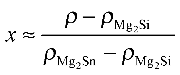 . We used the Archimedes density for this calculation as the geometrical density is prone to underestimate the Sn content in the case of open porosity in the samples. The thus calculated Sn content is lower than the nominal content of x = 0.2, but shows some increase with increase in the Sb concentration.
| Nominal composition | ρ geo [g cm−3] | ρ A [g cm−3] | x from ρA | x from XRD | |
|---|---|---|---|---|---|
| Mg2Si0.8Sn0.2 | #1 | 2.17 | 2.21 | 0.132 | 0.128 |
| Mg2Si0.795Sn0.2Sb0.005 | #2 | 2.25 | 2.24 | 0.145 | 0.140 |
| Mg2Si0.79Sn0.2Sb0.01 | #3 | 2.12 | 2.21 | 0.128 | 0.117 |
| Mg2Si0.785Sn0.2Sb0.015 | #4 | 2.33 | 2.31 | 0.174 | 0.170 |
| Mg2Si0.78Sn0.2Sb0.02 | #5 | 2.29 | 2.31 | 0.168 | 0.170 |
Fig. 1 shows the XRD results. All major peaks can be indexed according to the reported anti-fluorite structures (space group Fm![[3 with combining macron]](https://www.rsc.org/images/entities/char_0033_0304.gif) m) of Mg2Si and Mg2Sn. The minor peak at 2θ ≈ 43° corresponds to MgO, an impurity often observed in this material class.28 The zoom-in around the 220 peak in Fig. 1(b) shows that the peaks are relatively broad and show a shift towards smaller angles, i.e. larger lattice constants compared to Mg2Si.
m) of Mg2Si and Mg2Sn. The minor peak at 2θ ≈ 43° corresponds to MgO, an impurity often observed in this material class.28 The zoom-in around the 220 peak in Fig. 1(b) shows that the peaks are relatively broad and show a shift towards smaller angles, i.e. larger lattice constants compared to Mg2Si.
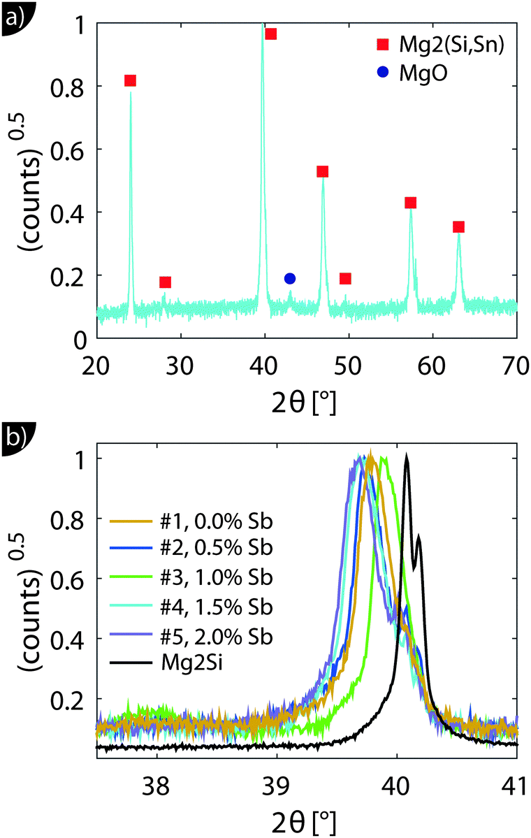 | ||
| Fig. 1 (a) X-ray diffraction data of sample #2. All major peaks can be indexed as (shifted) Mg2Si peaks. Minor peaks for MgO can also be observed. (b) The zoom-in around the (220) peak reveals peak broadening and emphasizes the shift compared to the Mg2Si sample. | ||
The relationship between the lattice constant a and Sn content x is approximately given by x = (a − aMg2Si)/(0.0427 nm).20 The calculated values of x are given in Table 1 and confirm the results and trends obtained from the density data. In fact, the good agreement between the Sn content obtained from density data and the XRD peak shift indicates good compaction and a high relative density of the samples, as significant (closed) porosity leads to a reduced x from the density data but does not affect that from the XRD peak shift.
Microstructural analysis by SEM shows a multiphase sample with a matrix in grey and minor phases in light grey and dark grey, as shown in Fig. 2. The image is taken for sample #5, but the microstructure is similar in all samples, see Fig. S2–S4 (ESI†). EDX analysis of all samples reveals that the matrix and the minor phases do not have sharp compositions, but consist of domains with similar, yet distinct local compositions.
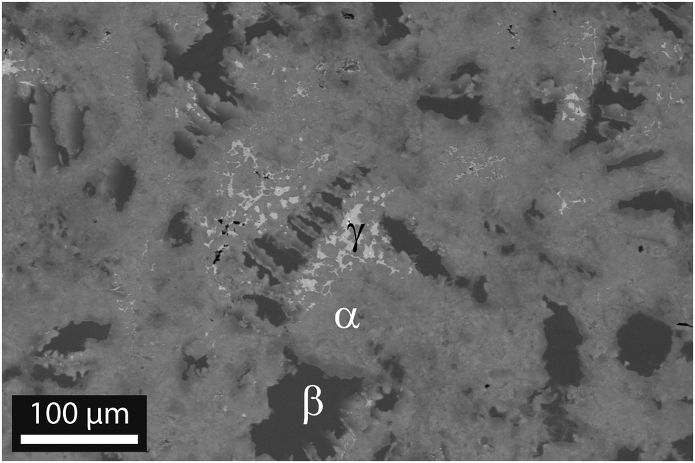 | ||
| Fig. 2 Backscattered image of sample #5. Three different phases are clearly distinguishable: the main phase α, the Mg2Si-like phase β and the Sn-rich phase γ. EDX analysis reveals that these phases show significant local concentration fluctuations. | ||
The Sn content x and the approximate phase fractions are given in Table 2. Employing the distinct grey values of the three phases, the graphical analysis software ImageJ has been used to estimate the (areal) fraction of each phase. It yields 85% main phase, 13% of the Mg2Si-like phase and about 2% for the Sn-rich phase for the two-dimensional image. To calculate the 3D values, we assumed that the main phase is the matrix and the minor phases are isotropically included within the matrix. The phase fraction for the minor phases is then given by z2D3/2, where z2D is the fraction in the two dimensional image.
| Main phase (α) | Si-rich phase (β, dark) | Sn-rich phase (γ, bright) | |
|---|---|---|---|
| Sn content x | 0.1 < x < 0.2 | x < 0.03 | 0.4 < x < 0.6 |
| Phase fraction | 0.95 | 0.05 | <0.01 |
Fig. 3 shows the element mapping of a typical Mg2Si0.8Sn0.2 sample. The Mg2Si-like and the main phase are clearly distinguishable, and it can also be seen that the matrix phase itself has a spatially varying Sn content. Another interesting feature is the observed difference in the Sb content for the main phase and the Mg2Si-like phase. Sb is significantly more dissolved in the main phase with a higher Sn content. Presumably Sb can be more easily incorporated in Sn-richer phases due to their larger lattice constant. The EDX analysis also detects some oxygen, mainly at interface regions between the matrix phase and the Mg2Si-like phase. As MgO has been identified by XRD it can be deduced that oxygen is present presumably in the form of MgO. The matrix phase and the Mg2Si like phase are also visible in the Mg mapping. As the lattice constant increases with increase in the Sn content, the Mg density is higher in the Mg2Si-like phase than in the matrix phase, which results in the observed contrast.
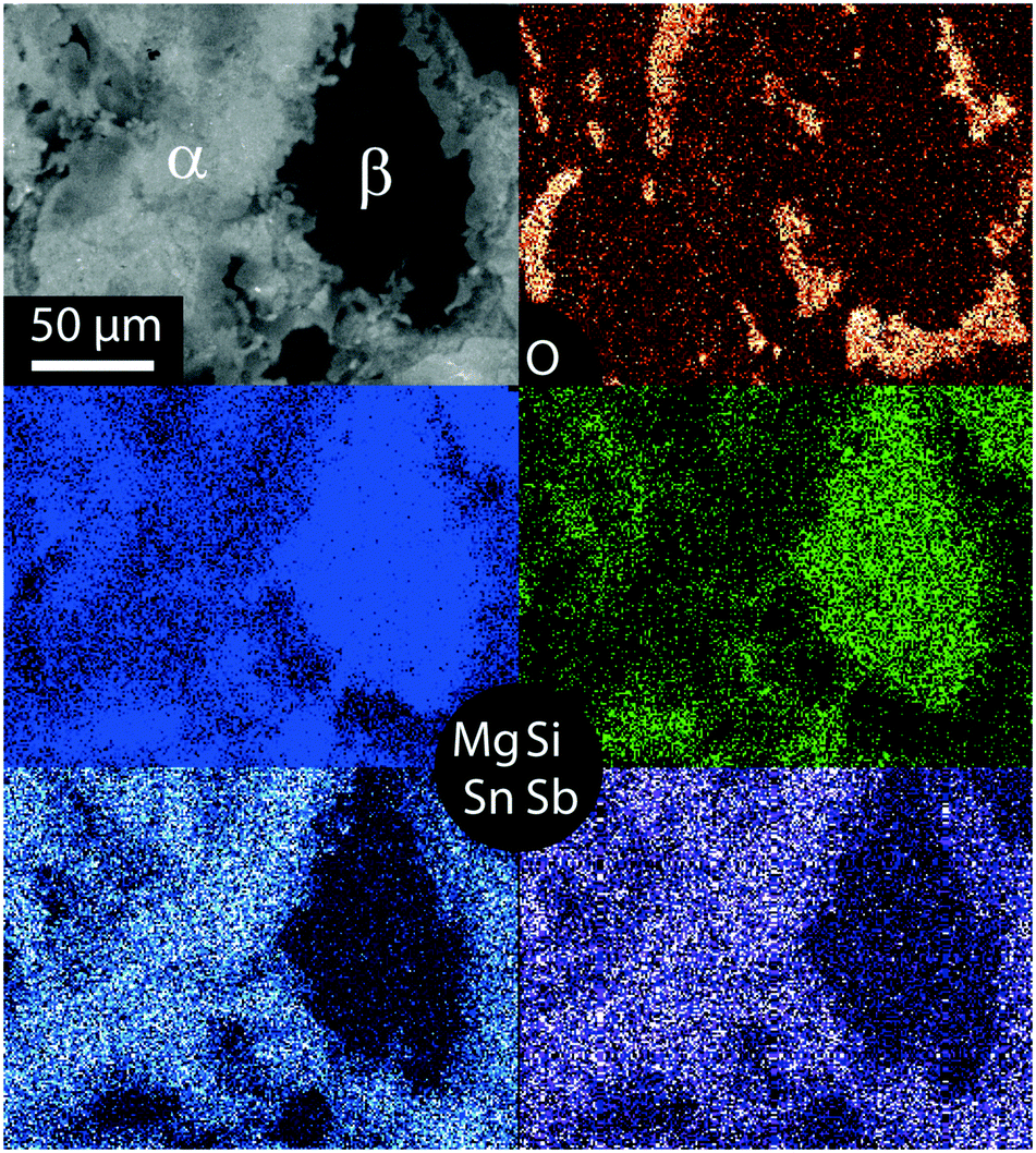 | ||
| Fig. 3 BSE image and elemental mapping of O, Mg, Si, Sn and Sb. | ||
Transport data
Despite the microstructure the samples exhibit a good macroscopic homogeneity of their electronic properties as evidenced by a local mapping of the Seebeck coefficient (see Fig. S6, ESI†).Transport data of Mg2Si0.8−ySn0.2Sby are shown from room temperature to 740 K in Fig. 4. Due to better visibility only the thermal conductivity data of the undoped sample (#1) are shown here; the complete data are presented in Fig. S5 of the ESI.† The electrical conductivity (a) shows the typical decrease with increase in the temperature of a highly doped semiconductor above 400 K; below 400 K a plateau can be observed for some of the samples. The electrical conductivity also exhibits the expected increase with increase in doping. The Seebeck coefficient (b) decreases with increase in doping and increases approximately linearly with increase in the temperature for all samples.
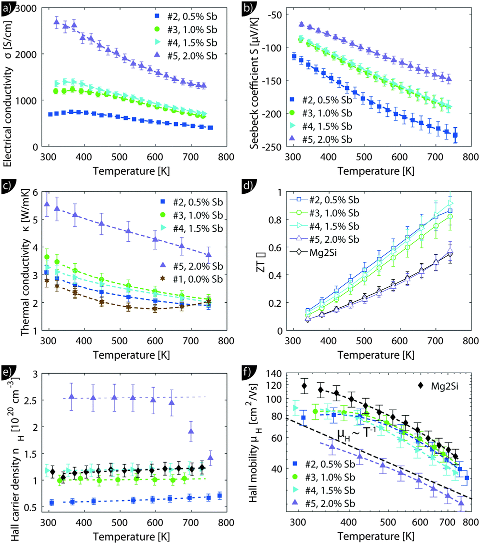 | ||
| Fig. 4 Transport measurement data for Mg2Si0.8−ySn0.2Sby samples. Full markers indicate measurement data, empty markers the calculated data and the dashed lines the fitted transport data that are used for modeling. The thermoelectric figure of merit (d) as well as the Hall carrier concentration (e) and mobility (f) are also presented for a sample with the composition Mg2Si0.9875Sb0.0125 (i.e. without tin) for comparison. This sample is labelled as “Mg2Si”. | ||
The thermal conductivity (c) decreases with temperature for all samples but shows a much higher value for the sample with the highest doping. The thermoelectric figure of merit ZT is calculated from (a) to (c) and shows an increase with temperature for all samples. Sample #4 with y = 0.015 has the highest thermoelectric figure of merit with ZT = 0.95 at 740 K. While the ZT values for the less doped samples are lower, but comparable, sample #5 has a drastically lower figure of merit. Fig. 4(e) reveals a roughly temperature independent carrier density of all samples, except for sample #5. Here the carrier concentration is roughly constant up to 650 K after which nH decreases rapidly. As the sample has been stable during the S–σ and LFA measurements beforehand, we do not know what caused the irreversible change in the sample. It can be seen that the carrier density data of the samples are consistent with the results for S and σ and that the control over the carrier concentration is not perfect as the actual Hall carrier concentration does not exactly follow the linear trend expected from the nominal doping composition. Doping is relatively effective as one would roughly expect 1.5 × 1020 cm−3 carriers for a nominal composition of Mg2Si0.79Sn0.2Sb0.01 if one carrier per Sb atom is provided. The Hall mobility (f) decreases with increase in the temperature after an initial plateau for samples #2–#4; sample #5 shows a monotonic trend with significantly lower absolute values.
We will now analyze the results in the framework of a single parabolic band model (SPB).29 This model has been employed for Mg2Si and Mg2Si1−xSnx with reasonable success beforehand.5,21,30 For T > 500 K μH ∝ T−p holds with 1 < p < 1.5, which indicates acoustic phonon (AP) scattering as the dominant scattering mechanism. At lower temperatures, there is some deviation from this behavior, presumably due to grain boundary scattering of the charge carriers at the interfaces.28 A possible influence of alloy scattering cannot be excluded, but is not expected to be dominant due to the relatively low Sn content.6 Grain boundary scattering is an extrinsic scattering mechanism so that AP scattering can assumed to be the dominant intrinsic mechanism at all temperatures. In this case, the reduced chemical potential η and the DOS effective mass m* of the electrons can be calculated using
 | (1) |
 | (2) |
 . The measured Hall carrier density nH is linked to the true carrier density by nH = n/rH with the Hall scattering factor given by
  . The chemical potentials for samples #2–#5 are plotted in Fig. 5(a). It can be seen that the chemical potential lies above the conduction band edge at room temperature for all samples. It decreases with increase in the temperature and crosses the band edge for the lowest doped sample.
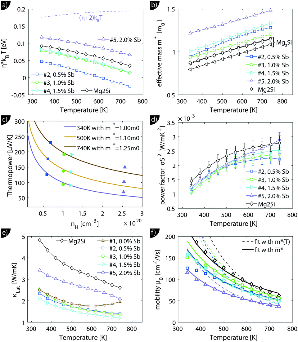 | ||
| Fig. 5 Results from the single parabolic band model for Mg2Si0.8−ySn0.2Sby; for comparison, the data of Mg2Si0.9875Sb0.0125 (“Mg2Si”) from ref. 28 are also presented. (a) Calculated chemical potential for all samples. For the sample with the largest carrier concentration (#5) (η + 2)kBT is plotted as well; this gives an impression up to which energy a significant number of carriers are excited. (b) All samples show an increase in the effective mass with increase in the temperature, with sample #5 having a significantly higher effective mass. (c) The Pisarenko plot shows decent agreement between experimental data and theoretical curves using the temperature dependent effective masses of (b). (d and e) Power factor σS2 and lattice thermal conductivity (overlaid by bipolar contribution). Compared to Mg2Si, the Mg2Si0.8Sn0.2 samples show a slightly reduced power factor but a drastically reduced lattice thermal conductivity. (f) A fit of the mobility parameter μ0vs. T can be used to obtain the deformation potential. Dashed lines show the results using m*(T) while the solid lines the results from an averaged effective mass. | ||
The effective mass increases with temperature for all samples. While the three lower doped samples increase roughly from 1m0 to 1.25m0 in the measured temperature range, the sample with the highest doping increases from 1.25m0 to 1.35m0; m0 is the free electron mass. The Pisarenko plot in Fig. 5(c) shows reasonable agreement between the experimental and the modeling data.
The lattice thermal conductivity (and the bipolar contribution) is plotted in Fig. 5(e). It is given by κlat + κbip = κ − LσT, with  for the SPB model with AP scattering. The thermal conductivities of samples #1–#4 are comparable with a slight reduction for increased doping. The lattice thermal conductivity follows the power law κlat = A + B/Tp with −1 < p < −0.5. Umklapp phonon scattering predicts a κlat ∝ T−1 behavior, while κlat ∝ T−0.5 corresponds to alloy scattering as the dominant phonon scattering mechanism. The measurement results therefore indicate a mixed scattering mechanism. At high temperature, the onset of the bipolar contribution is clearly visible for the undoped sample. The sample with the highest doping has a lattice thermal conductivity, which is more than 50%, higher than the others, indicating a significantly different thermal transport in this sample.
The carrier density independent mobility μ0 is plotted in Fig. 5(f) and is related to the Hall mobility by ref. 29. It is a material parameter and is thus supposed to be independent of the carrier concentration. Indeed one notices that the mobilities for samples #2–#4 are very similar. The mobility of sample #5 is significantly lower; however, the difference is not as large as for μH. The mobility data can be used to extract a further material parameter, the deformation potential Edef which quantifies the interaction between acoustic phonons and charge carriers. It is given by ref. 31:
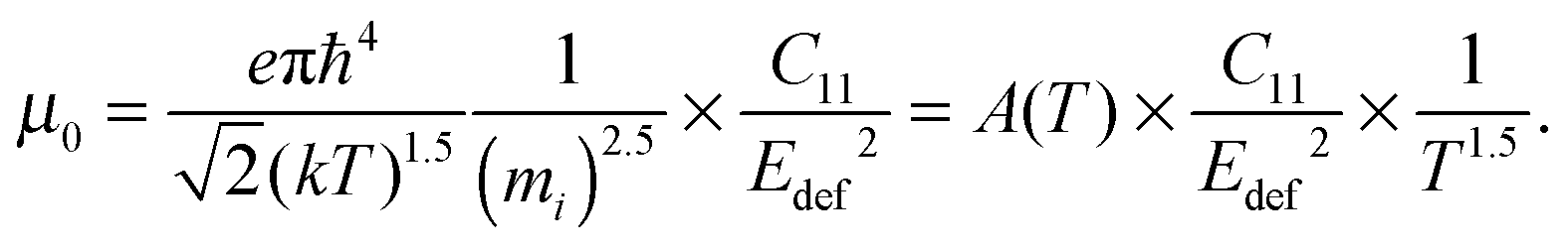 | (3) |
The thermoelectric potential of the material can be estimated by calculating ZT(n,T). The basic equation can be rearranged as
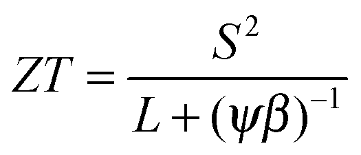 | (4) |
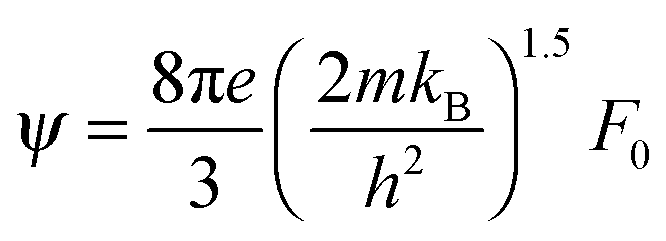 ,
, 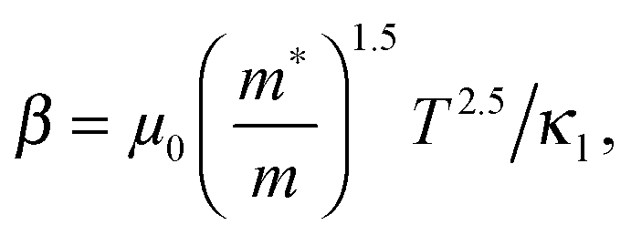 and μ0 = μH × 2F0/F−0.5. The material parameter β is plotted in Fig. S7d (ESI†). For the theoretical curves shown in Fig. 6, the average β of samples #2–#4 has been employed.
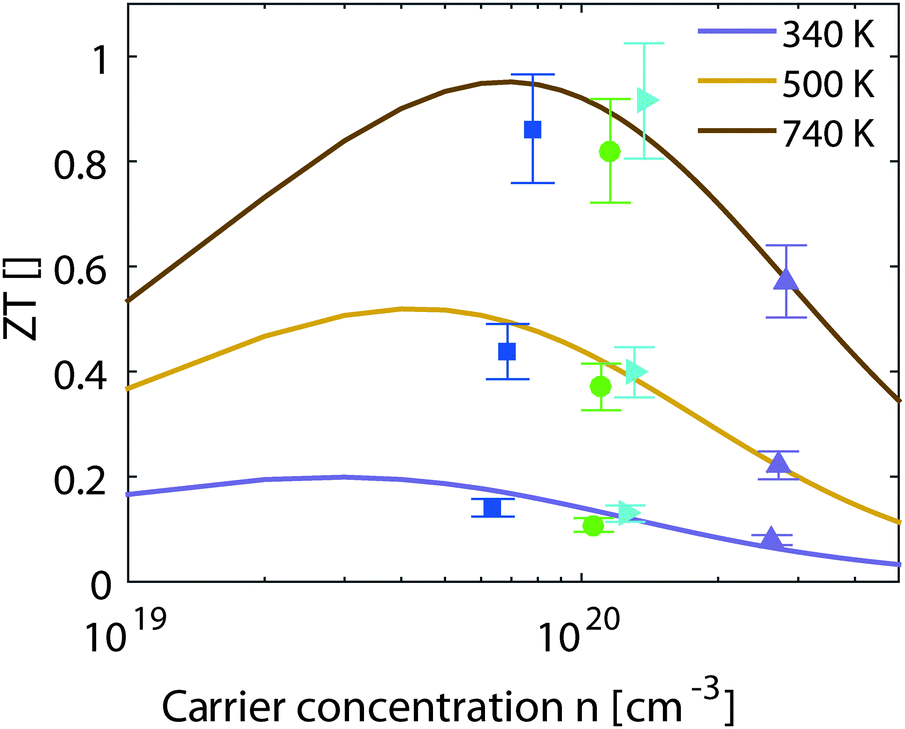 | ||
| Fig. 6 Experimental and theoretical results for the thermoelectric figure of merit vs. the carrier concentration at different temperatures. | ||
The results from eqn (4) show the expected trends: an increase in ZTmax with increasing temperature and a shift of the optimal carrier concentration towards higher values for increasing temperature. Our experimental data show good agreement with the modeling results. ZTmax obtained both from the SPB model and the experimental data is ≈0.95 at 740 K. The best experimental value is at nopt = 1.2 × 1020 cm−3, while the model predicts 0.7 × 1020 cm−3; however, the maximum is relatively broad and the model does not account for differences in κlat observed between the samples.
Discussion
Microstructure
The XRD and density measurements confirm the successful synthesis of Mg2Si1−x−ySnxSby with x ≈ 0.15. This is slightly smaller than that expected from the initial weight stoichiometry. We suspect that some elemental Sn is lost during the synthesis process. The Sn content values obtained from the XRD peak shift and from Archimedes density agree well with each other and show the same minor increase of x with increase in the dopant concentration. It is well known from other material classes (e.g. CoSb3 type skutterudites32) that small changes in the composition can influence the solubility of one of the components in the material. This is plausible in this case because the targeted composition is close to the edge of the reported miscibility gap. The electron microscope investigations reveal multiphase samples composed of three different phases. However, these phases are not homogeneous but consist of domains with a similar but distinct stoichiometry. The main phase has a Sn content of 0.1 < x < 0.2 and comprises of around 95% of the material volume. The second phase with 5 vol% is Mg2Si-like with x < 0.03. The third phase has <1 vol% and 0.4 < x < 0.6. These observations are in agreement with the reported miscibility gap between Mg2Si and Mg2Sn. Our results are also in quantitative agreement with the data from ref. 16 taking into account that EDX analysis gives a lower limit for x at the left side of the miscibility gap and an upper limit for the right side due to the limited spatial resolution.Our SEM/EDX results confirm the XRD results where the observed broad peaks indicate stoichiometric variations. The observed minor phases can very well be hidden in the shoulders of the broad peaks. EDX mapping also shows a lower content of the dopant Sb in the Mg2Si-like phase compared to the matrix phase. As the matrix phase has a slightly larger lattice constant a better Sb solubility can be expected.
Transport data
We have obtained ZTmax = 0.95 at 740 K, higher than previous reports on the same composition. Liu et al. and Samunin et al. both obtained a ZTmax around 0.8.5,12 The samples investigated by Liu et al. exhibit a slightly higher power factor than our samples but a significantly higher thermal conductivity. Tani et al. studied the composition Mg2Si0.9Sn0.1 and obtained a ZTmax = 0.68 at 864 K. Comparing our transport data with the work of Tani et al. on Mg2Si0.9Sn0.1, we find similar power factors but a higher lattice thermal conductivity in their work.11 A possible explanation is the intrinsic nanostructuring in our samples due to the existence of three distinct phases as well as the compositional variations within these phases. This characteristic has not been discussed in the previous reports; however, as no details on the microstructure are given in these reports a thorough comparison is difficult. We also note that our lattice thermal conductivities for samples #1–#4 are in good agreement with the experimental and theoretical results obtained at room temperature by Zaitsev et al.33 The significantly higher thermal conductivity of #5 has to be related to the microstructure of the sample; however, since microstructural investigations have not revealed a fundamental difference between #5 and #2–#4, further investigations are required.Electronic transport analysis
We have modeled the electronic transport properties within the SPB model with AP scattering as the dominant scattering mechanism. Overall the agreement of experimental data and modeling predictions is good. At low temperatures, the fingerprint of the second scattering mechanism is visible in σ, which can be related to the observed MgO in the samples. It has been shown that MgO can cause additional grain boundary scattering and hence reduce carrier mobility and electrical conductivity.28,34 The main parameters used in or extracted from the model are summarized in Table 3.| T | n opt [1019 cm−3] | ZT max | m* [m0] | κ lat [W mK−1] | E def [eV] |
|---|---|---|---|---|---|
| 340 | 3 | 0.2 | 1 | 2.3 | 13.0 |
| 740 | 7 | 0.95 | 1.25 | 1.3 | 13.0 |
We found an optimum carrier concentration nopt which is lower than the value (nopt = 18 × 1019 cm−3) stated by Liu et al.;5 however the carrier concentration optimization was mainly performed in view of compositions with a higher Sn content in their work. With respect to the effective mass we found good agreement with the literature reports: Liu et al. obtained m* = 0.93m0 for Mg2Si0.8Sn0.2, while Tani et al. obtained m* = 0.9m0 for Mg2Si0.9Sn0.1 at room temperature.
However, there are also deviations from the SPB model. Firstly, we observe an apparent increase of the carrier concentration (see Fig. 4 for nH(T) or Fig. S7(b) (ESI†) for n(T)). Secondly, we found a clear increase in the effective mass with temperature and a difference between the sample with the highest doping (#5) and the other samples. Thirdly, the carrier density corrected mobility μ0 differs for sample #5 compared to samples #2–#4 (see Fig. 5(f)), although it is a material parameter and is supposed to be independent of carrier concentrations.
The increase in n and m* with T was similarly found in Mg2Si28,30 and might be due to the non-parabolicity of the bands. The observed difference in m* for #5 compared to #2–#4 could be due to either a non-parabolic band or by the influence of the second conduction band with higher m*: Mg2Si1−xSnx has two threefold degenerate conduction bands CBL and CBH with a band gap E0 that depends on x. For small x the light conduction band is at a lower energy, while for large x the heavy band is at lower energy. The cross-over is around 0.6.5,10 The band gap between the two conduction bands is less clear for arbitrary x. Zaitsev et al. used E0,x=0 = 0.4 eV (with CBL closer to the valence band) and E0,x=1 = 0.2 eV (with CBH closer to the valence band). They suggested a linear interpolation in between which results in E0,x=0.2 = 0.28 eV.4 Bahk et al. used the same assumption for a recent transport modeling.20 On the other hand, Bourgeois et al. calculated E0,x=0 = 0.19 eV and E0,x=1 = 0.28 eV which correspond to E0,x=0.2 = 0.1 eV, i.e., a much smaller band gap for the investigated composition.15 Tan et al. calculated the interband gaps using DFT for different compositions obtaining E0,x=0.25 ≈ 0.3 eV.35 The discrepancy in the literature reports shows that the interband gap is not well characterized as the band positions are temperature dependent and the calculations do not account for this.
One possible explanation for the experimentally observed increase in m* for sample #5 compared to #2–#4 is thus a contribution of the second conduction band CBH to the electronic transport. If CBH is within (η + 2)kBT some contribution can be expected. Fig. 5(a) indicates that this would be the case for E0 < 0.2 eV. On the other hand, DFT calculations have shown that the bands of Mg2(Si,Sn) are not strictly parabolic and therefore the effective mass depends on the chemical potential.35,36 In this case, however, the density-of-states effective mass, which is related to the band shape, is not identical to the momentum effective mass (which controls the transport integrals) anymore.37 Considering only the effective mass data can thus not provide clear evidence on E0 and the question whether one or two bands contribute. Further insight can be gained by a detailed analysis of the mobility data. The fits of μ0(T) to extract the electron acoustic phonon interaction parameter Edef are plotted using m*(T), as shown in Fig. 5(f) as dashed lines. The fits are performed in the temperature region where AP scattering is clearly dominant, i.e. above 500 K. The agreement between experimental data and theoretical results is not very good, in particular with respect to the temperature dependence. As the strong temperature dependence of m*(T) is unexpected and might be an artifact of the assumed parabolic band structure we have also fitted the data using the average, temperature independent m* of each sample. The results are plotted in full lines and are in almost perfect agreement with the experimental data above 450 K. This indicates that the observed apparent increase in m*(T) is indeed an artifact of the simple SPB model assumptions.
The phonon deformation potential can be extracted from the fits if the elastic constant C11 is known. As this is not the case for this particular composition we have used a linear interpolation of the experimental room temperature values from Mg2Si and Mg2Sn, yielding C11,x=0.2 ≈ 110 GPa.38,39 This is in decent agreement with preliminary data obtained from resonant ultrasonic spectroscopy giving ≈100 GPa.40 The fitting results for Edef of samples #2–#5 are 13.1 eV, 13.5 eV, 12.8 eV, 12.8 eV, respectively, giving an average value of Edef,x=0.2 = 13.0 eV. The good agreement between the results for each sample (although μ0 is different) firstly increases the credibility of the result for Edef,x=0.2 and secondly argues against a significant influence of the second band CBH on the electronic transport: as the deformation potential for the two sub-bands differs by more than 50%,6 one should see a difference in Edef between #5 and samples #2–#4. This as well as the much better fits of μ0(T) for a temperature-independent m* indicate that the observed differences in the mobility parameter μ0 between the samples and the apparent temperature dependent m* are rather the consequences of a not strictly parabolic band CBL than due to the second band contributing to the transport.
Our result for Edef is higher than the value used by Bahk et al.: Edef,x=0.2 = 8.9 eV. The difference is not due to the mobility data but rather the used elastic constant. Bakh et al. used C11,x=0.2 ≈ 40 GPa, i.e. a much lower value. If we use the same elastic constant we obtain Edef,x=0.2 ≈ 7.9 eV in good agreement with their data. This disagreement can be figured out by mapping of the elastic constants with temperature and composition. Liu et al. obtained Edef,x=0 = 17 eV and Edef,x=1 = 10 eV, which give Edef,x=0.2 = 15.4 eV in the linear interpolation; in decent agreement with our results.6
Comparison with Mg2Si
Further insight into fundamental trends can be gained by comparing the obtained material parameters of Mg2Si0.8Sn0.2 with those of the parental compound Mg2Si. We have therefore plotted the relevant transport data and modeling results of a sample with composition Mg2Si0.9875Sb0.0125 in Fig. 4 and 5, labelled as “Mg2Si”. The dopant concentration and compaction parameters were optimized giving ZT > 0.7 at 800 K, the sample might therefore serve as a valid comparison.23,28,41 The formation of a solid solution and the observed multiphase character of the Mg2Si0.8Sn0.2 samples affect the power factor only to a small extent but reduce the lattice thermal conductivity by a factor of 2 over the whole measurement range. The general trends are not unexpected and have been observed previously.4,5 We furthermore observe a small reduction in charge carrier mobility, which is partly due to additional alloy scattering at the Sn atoms42 and partly due to the microstructure. The more fundamental question is: if and how variations in stoichiometry influence the band structure? In the model employed by Zaitsev and others, a change in the Si/Sn ratio results in a shift of conduction bands CBL and CBH with respect to each other (and the valence bands) but the curvature of the bands remains unaffected.4,5,20 Our measurement results indicate differently as we find an increase in the effective mass upon Sn substitution (see Fig. 5(b)), indicating a flattening of the CBL band. The increase in the effective mass with increase in the Sn content is in agreement with DFT results reported by Tan et al.35 We furthermore observe a slight reduction of the deformation potential. The mean value for Mg2Si0.8Sn0.2 is Edef,x=0.2 = 13.0 eV, while we found Edef,x=0 = 15 eV for the compound without Sn; see Fig. 5(f) and ref. 28.Overall, the main features of the electronic transport can be well understood in the framework of a single parabolic band, although the material is not a single phase compound and has a complex microstructure. It is plausible that the matrix phase is dominant for the carrier transport as the Sn-rich phase has only a very small volume fraction (<1%) and the Mg2Si-like phase is significantly less doped and therefore behaves more or less like insulating particles within the matrix. The dependence of m*(T,η) indicates that the bands are not strictly parabolic. Nevertheless, the agreement between experimental data and the predictions from the simple single parabolic band model is good and the material parameters like nopt, ZTmax, m*, Edef can expected to be reasonably accurate. The observed deviations from the single parabolic band model point towards a non-parabolic band, rather than a contribution from the second band. This indicates a band gap between the light and the heavy conduction band of ≥0.2 eV, supporting an earlier work by Zaitsev et al.4 and calculations by Liu et al.,5 but in contradiction to theoretical results by Bourgeois et al.15 However, the effect of the second band cannot be totally excluded from the data. We also note that a Kane type band would lead to a lower Seebeck coefficient at high doping than a parabolic band, in contrast to what is found experimentally. More sophisticated modeling is therefore required for a full assessment of the band structure.
Comparing the properties of Mg2Si0.8Sn0.2 with those of Mg2Si, we reveal a reduction of the phonon deformation potential and an increase in the effective mass, indicating a band flattening upon Sn substitution.
Conclusions
We have successfully synthesized Mg2Si0.8−ySn0.2Sby. The samples show a heterogeneous microstructure and a multiphase character. The main phase itself does not have one strict composition but is composed of various domains with similar compositions. We determine a maximum thermoelectric figure of merit of 0.95 at 740 K, the best reported for this composition. The specific figure of merit is comparable to the results for Mg2Si0.4Sn0.6; Mg2Si0.8Sn0.2 might thus find an application where the material weight is a crucial factor, i.e. in airborne applications. We furthermore show that the electronic transport can be modelled within a simple single parabolic model with reasonable accuracy. This allows for the extraction of fundamental material parameters like effective mass and the phonon deformation potential. Comparison with Mg2Si shows a flattening of the light conduction band, indicating that substitution of Si by Sn does not only affect the band energies but also their curvature.Acknowledgements
The authors would like to thank W. Schönau and P. Blaschkewitz for support with the thermoelectric measurements, and A. Francke and P. Watermeyer for their help with the electron microscope. Furthermore, B. Klobes is acknowledged for useful discussion on elastic constants and K. Kelm for discussion on microstructure and phase diagrams. Special thanks to Jeff Snyder for insights into band structures and effective masses as well as to the Helmholtz Association for endorsement.References
- G. S. Snyder and E. S. Toberer, Nat. Mater., 2008, 7, 105–114 CrossRef CAS PubMed.
- W. Choi, S. Hong, J. T. Abrahamson, J. H. Han, C. Song, N. Nair, S. Baik and M. S. Strano, Nat. Mater., 2010, 9, 423–429 CrossRef CAS PubMed.
- S. Walia, S. Balendhran, P. Yi, D. Yao, S. Zhuiykov, M. Pannirselvam, R. Weber, M. S. Strano, M. Bhaskaran, S. Sriram and K. Kalantar-zadeh, J. Phys. Chem. C, 2013, 117, 9137–9142 CAS.
- V. K. Zaitsev, M. I. Fedorov, E. A. Gurieva, I. S. Eremin, P. P. Konstantinov, A. Y. Samunin and M. V. Vedernikov, Phys. Rev. B: Condens. Matter Mater. Phys., 2006, 74, 045207 CrossRef.
- W. Liu, X. J. Tan, K. Yin, H. J. Liu, X. F. Tang, J. Shi, Q. J. Zhang and C. Uher, Phys. Rev. Lett., 2012, 108, 166601 CrossRef.
- X. H. Liu, T. J. Zhu, H. Wang, L. P. Hu, H. H. Xie, G. Y. Jiang, G. J. Snyder and X. B. Zhao, Adv. Energy Mater., 2013, 3, 1238–1244 CrossRef CAS PubMed.
- W. Liu, X. Tang and J. Sharp, J. Phys. D: Appl. Phys., 2010, 43, 085406 CrossRef.
- A. U. Khan, N. V. Vlachos, E. Hatzikraniotis, G. S. Polymeris, C. B. Lioutas, E. C. Stefanaki, K. M. Paraskevopoulos, I. Giapintzakis and T. Kyratsi, Acta Mater., 2014, 77, 43–53 CrossRef CAS PubMed.
- P. Gao, I. Berkun, R. Schmidt, M. Luzenski, X. Lu, P. Bordon Sarac, E. Case and T. Hogan, J. Electron. Mater., 2013, 1–14, DOI:10.1007/s11664-013-2865-8.
- T. Dasgupta, C. Stiewe, J. de Boor and E. Müller, Phys. Status Solidi A, 2014, 1250–1254, DOI:10.1002/pssa.201300196.
- J.-i. Tani and H. Kido, J. Alloys Compd., 2008, 466, 335–340 CrossRef CAS PubMed.
- A. Y. Samunin, V. K. Zaitsev, P. P. Konstantinov, M. I. Fedorov, G. N. Isachenko, A. T. Burkov, S. V. Novikov and E. A. Gurieva, J. Electron. Mater., 2013, 42, 1676–1679 CrossRef CAS.
- T. Sakamoto, T. Iida, Y. Honda, M. Tada, T. Sekiguchi, K. Nishio, Y. Kogo and Y. Takanashi, J. Electron. Mater., 2012, 41, 1805–1810 CrossRef CAS.
- J. de Boor, C. Gloanec, H. Kolb, R. Sottong, P. Ziolkowski and E. Müller, J. Alloys Compd., 2015, 632, 348–353 CrossRef CAS PubMed.
- J. Bourgeois, J. Tobola, B. Wiendlocha, L. Chaput, P. Zwolenski, D. Berthebaud, Q. Recour, F. Gascoin and H. Scherrer, Funct. Mater. Lett., 2013, 06, 1340005 CrossRef.
- S. F. Muntyanu, E. B. Sokolov and E. S. Makarov, Zh. Neorgan. Mater., 1966, 2, 870–875 CAS.
- A. Kozlov, J. Grobner and R. Schmid-Fetzer, J. Alloys Compd., 2011, 509, 3326–3337 CrossRef CAS PubMed.
- L. D. Zhao, V. P. Dravid and M. G. Kanatzidis, Energy Environ. Sci., 2014, 7, 251–268 CAS.
- W. J. Xie, J. He, S. Zhu, X. L. Su, S. Y. Wang, T. Holgate, J. W. Graff, V. Ponnambalam, S. J. Poon, X. F. Tang, Q. J. Zhang and T. M. Tritt, Acta Mater., 2010, 58, 4705–4713 CrossRef CAS PubMed.
- J. H. Bahk, Z. X. Bian and A. Shakouri, Phys. Rev. B: Condens. Matter Mater. Phys., 2014, 89, 075204 CrossRef.
- W. Liu, H. Chi, H. Sun, Q. Zhang, K. Yin, X. Tang, Q. Zhang and C. Uher, Phys. Chem. Chem. Phys., 2014, 16, 6893–6897 RSC.
- T. Dasgupta, C. Stiewe, R. Hassdorf, A. J. Zhou, L. Boettcher and E. Mueller, Phys. Rev. B: Condens. Matter Mater. Phys., 2011, 83, 235207 CrossRef.
- J. de Boor, C. Compere, T. Dasgupta, C. Stiewe, H. Kolb, A. Schmitz and E. Mueller, J. Mater. Sci., 2014, 49, 3196–3204 CrossRef CAS.
- J. de Boor, C. Stiewe, P. Ziolkowski, T. Dasgupta, G. Karpinski, E. Lenz, F. Edler and E. Mueller, J. Electron. Mater., 2013, 42, 1711–1718 CrossRef.
- J. de Boor and E. Muller, Rev. Sci. Instrum., 2013, 84, 065102 CrossRef CAS PubMed.
- L. J. van der Pauw, Philips Res. Rep., 1958, 13, 1–9 Search PubMed.
- K. A. Borup, J. de Boor, H. Wang, F. Drymiotis, F. Gascoin, X. Shi, L. Chen, M. I. Fedorov, E. Muller, B. B. Iversen and G. J. Snyder, Energy Environ. Sci., 2015, 8, 423–435 CAS.
- J. de Boor, T. Dasgupta, H. Kolb, C. Compere, K. Kelm and E. Mueller, Acta Mater., 2014, 77, 68–75 CrossRef CAS PubMed.
- A. F. May and G. J. Snyder, in Thermoelectrics and its Energy Harvesting, ed. D. M. Rowe, CRC Press, 2012, ch. 11 Search PubMed.
- S. K. Bux, M. T. Yeung, E. S. Toberer, G. J. Snyder, R. B. Kaner and J. P. Fleurial, J. Mater. Chem., 2011, 21, 12259–12266 RSC.
- A. F. May, E. S. Toberer, A. Saramat and G. J. Snyder, Phys. Rev. B: Condens. Matter Mater. Phys., 2009, 80, 125205 CrossRef.
- Y. L. Tang, Y. T. Qiu, L. L. Xi, X. Shi, W. Q. Zhang, L. D. Chen, S. M. Tseng, S. W. Chen and G. J. Snyder, Energy Environ. Sci., 2014, 7, 812–819 CAS.
- M. I. Fedorov and V. K. Zaitsev, in CRC Handbook of thermoelectrics: Macro to Nano, ed. D. M. Rowe, CRC, Boca Raton, USA, 2006, p. 31 Search PubMed.
- S. Fiameni, S. Battiston, S. Boldrini, A. Famengo, F. Agresti, S. Barison and M. Fabrizio, J. Solid State Chem., 2012, 193, 142–146 CrossRef CAS PubMed.
- X. J. Tan, W. Liu, H. J. Liu, J. Shi, X. F. Tang and C. Uher, Phys. Rev. B: Condens. Matter Mater. Phys., 2012, 85, 205212 CrossRef.
- D. A. Pshenai-Severin, M. I. Fedorov and A. Y. Samunin, J. Electron. Mater., 2013, 42, 1707–1710 CrossRef CAS.
- W. Zawadzki, Adv. Phys., 1974, 23, 435–522 CrossRef CAS PubMed.
- W. B. Whitten, P. L. Chung and G. C. Danielson, J. Phys. Chem. Solids, 1965, 26, 49–56 CrossRef CAS.
- L. C. Davis, W. B. Whitten and G. C. Danielson, J. Phys. Chem. Solids, 1967, 28, 439–447 CrossRef CAS.
- B. Klobes, personal communication.
- Y. Hayatsu, T. Iida, T. Sakamoto, S. Kurosaki, K. Nishio, Y. Kogo and Y. Takanashi, J. Solid State Chem., 2012, 193, 161–165 CrossRef CAS PubMed.
- H. Wang, A. D. LaLonde, Y. Z. Pei and G. J. Snyder, Adv. Funct. Mater., 2013, 23, 1586–1596 CrossRef CAS PubMed.
Footnotes |
| † Electronic supplementary information (ESI) available. See DOI: 10.1039/c5tc01535a |
| ‡ Contributed equally. |
| This journal is © The Royal Society of Chemistry 2015 |