Hydroxyl radical-assisted decomposition and oxidation in solution-processed indium oxide thin-film transistors
Received
21st May 2015
, Accepted 17th June 2015
First published on 18th June 2015
Abstract
Solution-processed indium oxide TFTs were fabricated by hydroxyl radical-assisted (HRA) decomposition and oxidation. The results show that decomposition and oxidation of carbon is more substantial than metal hydroxides, leading to the elimination of organic residues, correlated to a low interface trap density (S.S. = 0.45 V dec−1, NT = 1.11 × 1012 cm−2) in the device. The resultant HRA indium oxide TFTs exhibit improved electrical characteristics such as the mobility, the on/off current ratio, and the subthreshold swing as well as bias stabilities under PBS and NBS conditions.
Introduction
Their superior optical transparency and excellent charge transport characteristics make amorphous metal oxide semiconductors suitable for applications in flat panel displays and particularly thin-film transistors (TFTs).1 Vacuum-based deposition techniques are primarily employed to fabricate metal oxide as the channel layers in TFTs.2 However, as these vacuum-based techniques are costly from the aspect of machinery,3 solution-based techniques have been proposed as the alternative fabrication method.4 In addition, solution processing enables low temperature fabrication, high throughput, and large area deposition for metal oxide TFTs.
Along with the breakthrough of solution-processed metal oxide TFTs, a study on solution-processed heavy post transition metal cations in the form of oxide compounds has also been carried out.5 Among oxide compounds that include binary (ZnO, SnO2, In2O3), ternary (InZnO, ZnSnO), and quaternary (InGaZnO) compounds, indium oxide (In2O3) is one of the most studied materials as channel layers due to its high mobility of ∼10–65 cm2 V−1 s−1.6 Despite reports on high mobility,7–12 one challenge of In2O3 as the channel layer of the TFT is its volatility to poor bias durability due to high charge defects. These charge defects include metal interstitials, oxygen deficiencies, and carbon impurities. For In2O3, oxygen deficiency formation is inevitable owing to its low formation energy,13 and therefore oxygen binders such as Hf, W, and Si must be doped to achieve a low trap density which leads to high quality In2O3-based films.14,15 The addition of dopants requires higher annealing temperatures to achieve a satisfactory level of field effect mobility as that of undoped In2O3. It is therefore advantageous to produce In2O3 TFTs without using dopants to maintain low annealing temperatures. However, obtaining In2O3 TFTs with high field effect mobility combined with excellent bias stability at low annealing temperatures as well as without metal dopants remains a challenge.
Herein, we demonstrate the fabrication of In2O3 TFTs using hydroxyl radical-assisted (HRA) decomposition and oxidation. The generation of hydroxyl radicals was accomplished by incorporating and activating hydrogen peroxide in the In2O3 precursor solution. Different from our previous study which focused on general hydrogen peroxide doping,16 this study focuses on hydroxyl radical-assisted decomposition and oxidation. Moreover, we employ a significantly lower annealing temperature suitable for flexible substrates. By using the HRA method, we successfully produce In2O3 films with low trap sites and TFT characteristics exhibiting excellent field effect mobility and stabilities at a low temperature of 240 °C. In this report, we discuss the HRA decomposition and oxidation of In2O3 TFTs and characterize their electrical performance and stabilities.
Experimental
A 0.3 M indium oxide solution was made by dissolving indium nitrate hydrate (In[NO3]3·xH2O) in 10 mL of 2-methoxyethanol (2ME). Then, nitric acid (HNO3) was added. The precursor solution was stirred at 320 rpm for 4 hours and maintained at a temperature of 60 °C to create a homogeneous and transparent solution. Following that, the prepared solution was filtered through a 0.2 μm micro filter and spin-coated at 3000 rpm onto a substrate to form the active layer of thin-film transistors (TFTs). A total of four samples were prepared: (1) pristine In2O3, (2) In2O3–H2O2, (3) In2O3–HRA, and (4) In2O3–UV. For pristine In2O3 TFTs, the solution is coated as it is. For In2O3–H2O2 TFTs, 30% volume hydrogen peroxide (H2O2) was dispersed in pristine In2O3 solution. For In2O3–HRA TFTs, In2O3–H2O2 films were irradiated for 30 minutes with ultraviolet (UV) lamps with wavelengths of 185 nm and 254 nm at an intensity of 60 mW cm−2 to generate hydroxyl radicals (OH˙). To exclude the effect of UV light, pristine In2O3 was also irradiated following the same UV illumination procedure, herein referred to as In2O3–UV. All fabricated TFTs employed a bottom-gate, top-contact configuration. SiO2/p+-Si substrates (120 nm) were used as gate dielectrics/gate. The coated active layer was annealed at 240 °C for 4 hours on a hot plate in ambient air. The source and drain electrodes (Al, 100 nm) were then deposited using a thermal evaporator with a shadow mask. The channel of the fabricated TFT devices was 1000 μm wide and 150 μm long.
Current–voltage (I–V) characteristics of TFTs were measured at room temperature in a dark room using an HP4156C semiconductor parameter analyzer. Bias stability (positive bias stability, PBS; and negative bias stability, NBS) was recorded under the constant positive (+20 V) and negative (−20) gate bias for 1000 s at room temperature. VDS was set to 10.1 V and VG was swept from −30 V to 30 V to measure the stability. Chemical compositions of the oxide films were determined by Attenuated Total Reflection Fourier Transform Infrared (ATR-FTIR, Bruker Vertex 70) spectroscopy, X-ray Photoelectron Spectroscopy (XPS, Thermo VG Scientific), and Electron Spin Resonance (ESR, Bruker BioSpin) spectroscopy. The FTIR data were measured in reflection mode at a resolution of 4 cm−1. The XPS data were recorded using a monochromatic Al K source (1486.6 eV) in an ultra-high vacuum system at a base pressure of ∼10−10 Torr. The C 1s peak at 284.8 eV was used for calibration. For ESR spectroscopy, spin-trapping was used due to the low concentration and the transient nature of the radicals. 5,5-Dimethyl-1-pyrroline N-oxide (DMPO) was chosen as a spin trap agent because of its well-documented trapping ability and selectivity for radicals.17–19
Results and discussion
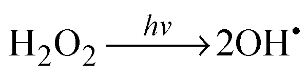
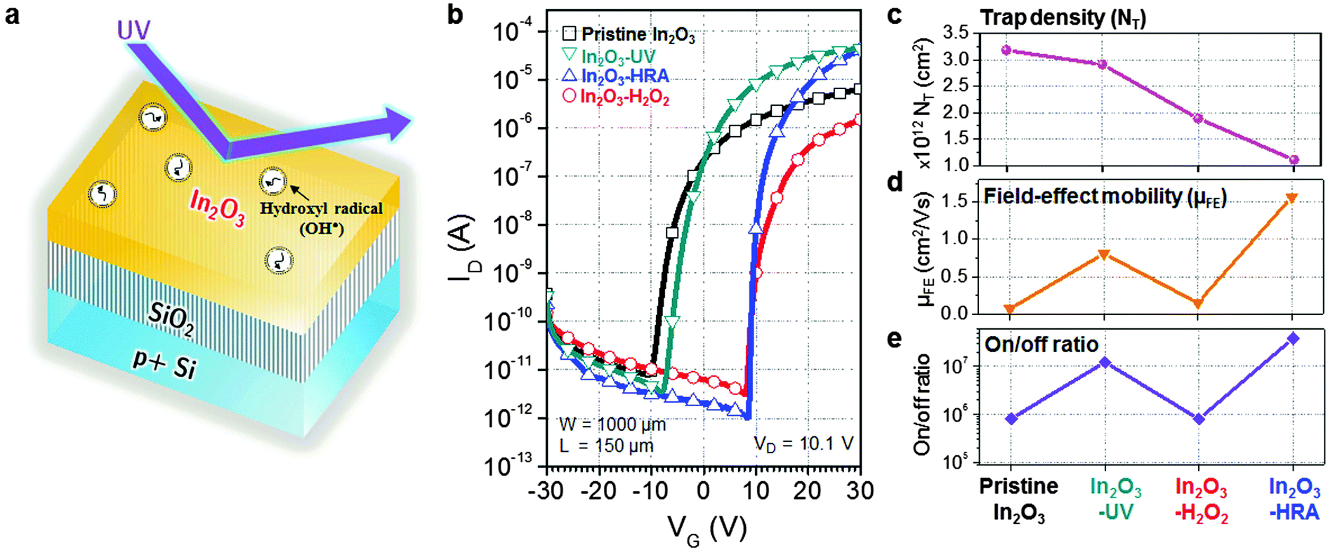
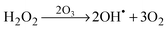
The schematic illustration of the HRA decomposition and oxidation method is shown in Fig. 1a. OH˙ can be generated through UV irradiation because H2O2 absorbs wavelengths ≤350 nm subsequently causing photolytic cleavage to yield OH˙.19–21 The irradiation generates two OH˙ per molecule of H2O2 as shown in eqn (1). In this photocatalytic reaction, OH˙ was produced as main species through photocatalysis.| |  | (1) |
 |
| | Fig. 1 (a) Schematic of a hydroxyl radical-assisted (HRA) method for solution-processed In2O3 thin-films. (b) Transfer characteristics of bottom-gate, top-contact In2O3 TFTs with the channel width W = 1000 μm and the channel length L = 150 μm. (c) Trap density, (d) field-effect mobility, and (e) the on/off ratio of the In2O3 TFTs. | |
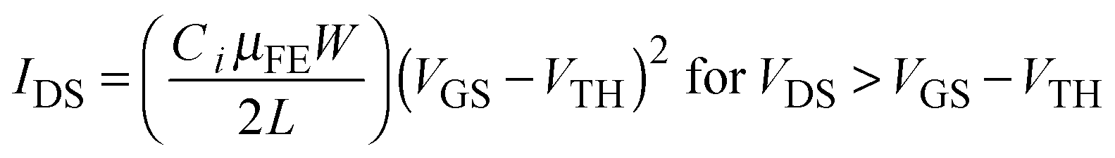
Fig. 1b displays the transfer characteristics of pristine In2O3, In2O3–UV, In2O3–H2O2, and In2O3–HRA TFTs, and Table 1 summarizes their representative electrical parameters. The electrical parameters were extracted from transfer curves in the saturation regime using the transconductance (gm) method:
| |  | (2) |
where
W is the channel width,
L is the channel length, and
Ci is the capacitance per unit area of the dielectric layer. HRA decomposition and oxidation results in the most decrease of the trap density and distinctly higher mobility with a better on/off current ratio. As the trap density (
NT) was calculated from the subthreshold swing (S.S.), the decrease in the trap density also correlates to the improvement in the S.S. performance. In contrast, incorporation of energetic (4.88–6.70 eV) UV illumination without OH˙ may not decrease trap sites as shown for the In
2O
3–UV device. It is therefore commonly accepted that excess trap sites may occur due to the high excitation energy and ozone formation from UV illumination. The result implies that the HRA method both effectively reduces defects related to trap sites and sub-gap states and enhances the electrical characteristics such as the mobility, the on/off current ratio, and the S.S.
Table 1 Summary of electrical parameters of solution-processed In2O3 TFTs
| Devices |
Mobility (cm2 V−1 s−1) |
S.S. (V dec−1) |
N
T (cm−2) |
On/off ratio |
| Pristine In2O3 |
0.07 |
1.17 |
3.18 × 10¹² |
8.13 × 10⁵ |
| In2O3–UV |
0.81 |
1.08 |
2.91 × 10¹² |
1.23 × 10⁷ |
| In2O3–H2O2 |
0.15 |
0.72 |
1.89 × 10¹² |
8.02 × 10⁵ |
| In2O3–HRA |
1.57 |
0.45 |
1.11 × 10¹² |
3.88 × 10⁷ |
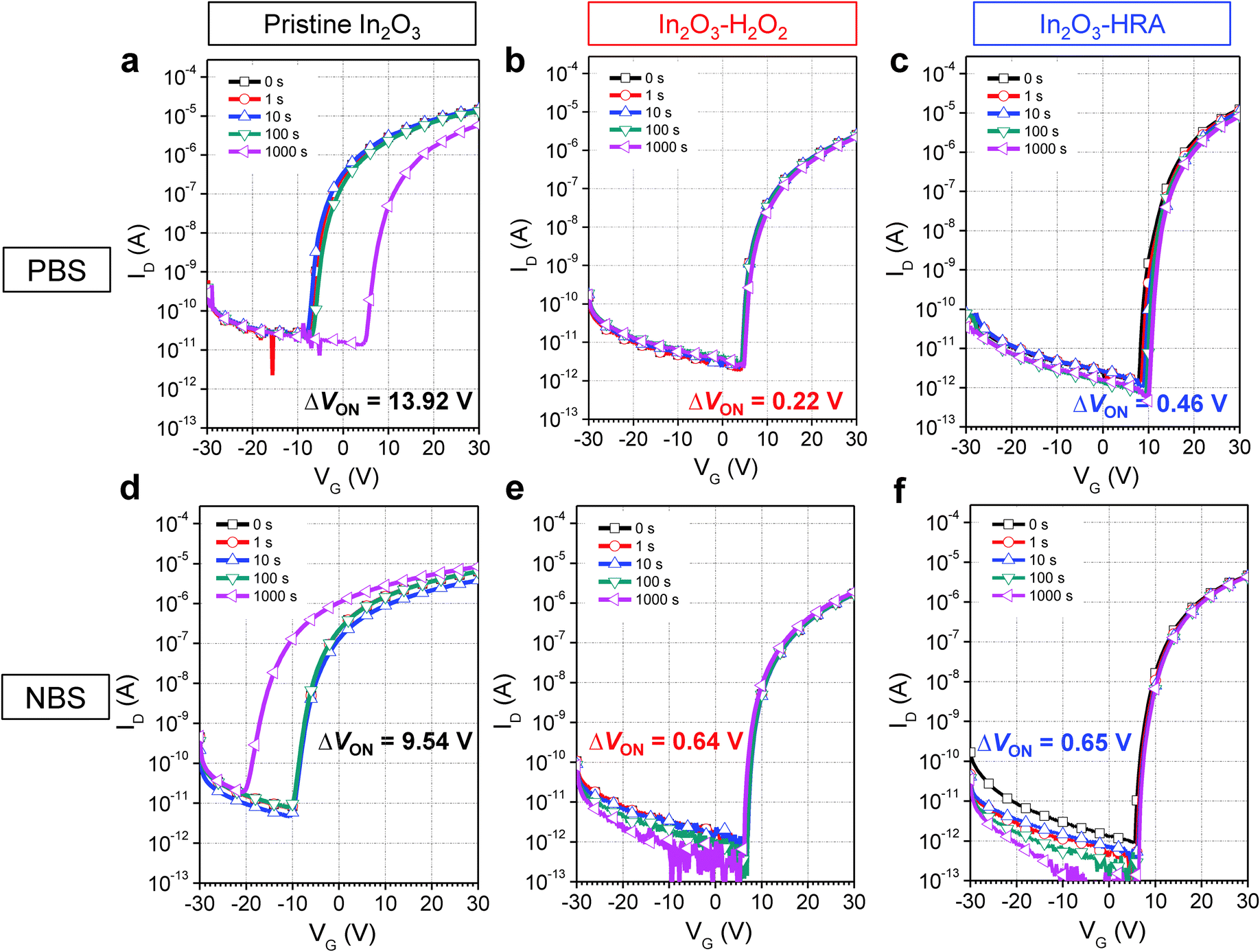
To verify the trap density reduction behavior, bias stabilities of pristine In2O3, In2O3–H2O2, and In2O3–HRA TFTs were investigated under PBS and NBS conditions (Fig. 2). The In2O3–HRA TFT showed a shift of 0.46 V upon the PBS and 0.65 V upon the NBS after 1000 s. The instability of electrical properties under bias stress can be explained by two general mechanisms: (1) the defect creation model and (2) the charge trapping model. In the defect creation model, VON shifts with deterioration of S.S. as a result of gate bias stress that induces formation of trap sites. In the charge trapping model, on the other hand, VON shifts without deterioration of S.S. It is widely believed that the VON shift (ΔVON) is contributed by charges trapped at the dielectric/channel interface and inside the bulk of the channel, resulting in ΔVON without a significant change in S.S. The charge trapping model is related to ΔVON (ΔVON = VON,Final − VON,Initial) and stress time using the stretched-exponential equation:22,23
| | ΔVON = ΔVON0![[thin space (1/6-em)]](https://www.rsc.org/images/entities/char_2009.gif) [1 − exp{−(t/τ)β}] [1 − exp{−(t/τ)β}] | (3) |
where
V0 is the
VON at the start of the experiment,
τ is the characteristic trapping time of electron carriers,
t is the stress duration time, and
β is
T/
T0. As shown in
Fig. 2, transfer curves of the In
2O
3–HRA TFT show no degradation of S.S. and only a small parallel shift. This result indicates that the In
2O
3–HRA TFT shows prominent improvements under both PBS and NBS conditions compared to the pristine In
2O
3 device owing to reduced trap sites.
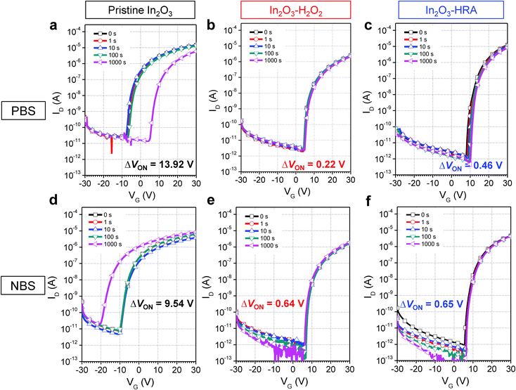 |
| | Fig. 2 Evaluation with positive bias stress (a–c) and negative bias stress (d–f) for pristine In2O3, (a) and (d); In2O3–H2O2, (b) and (e); and In2O3–HRA, (c) and (f); with a gate voltage of 20 V and −20 V respectively for 1000 s. | |
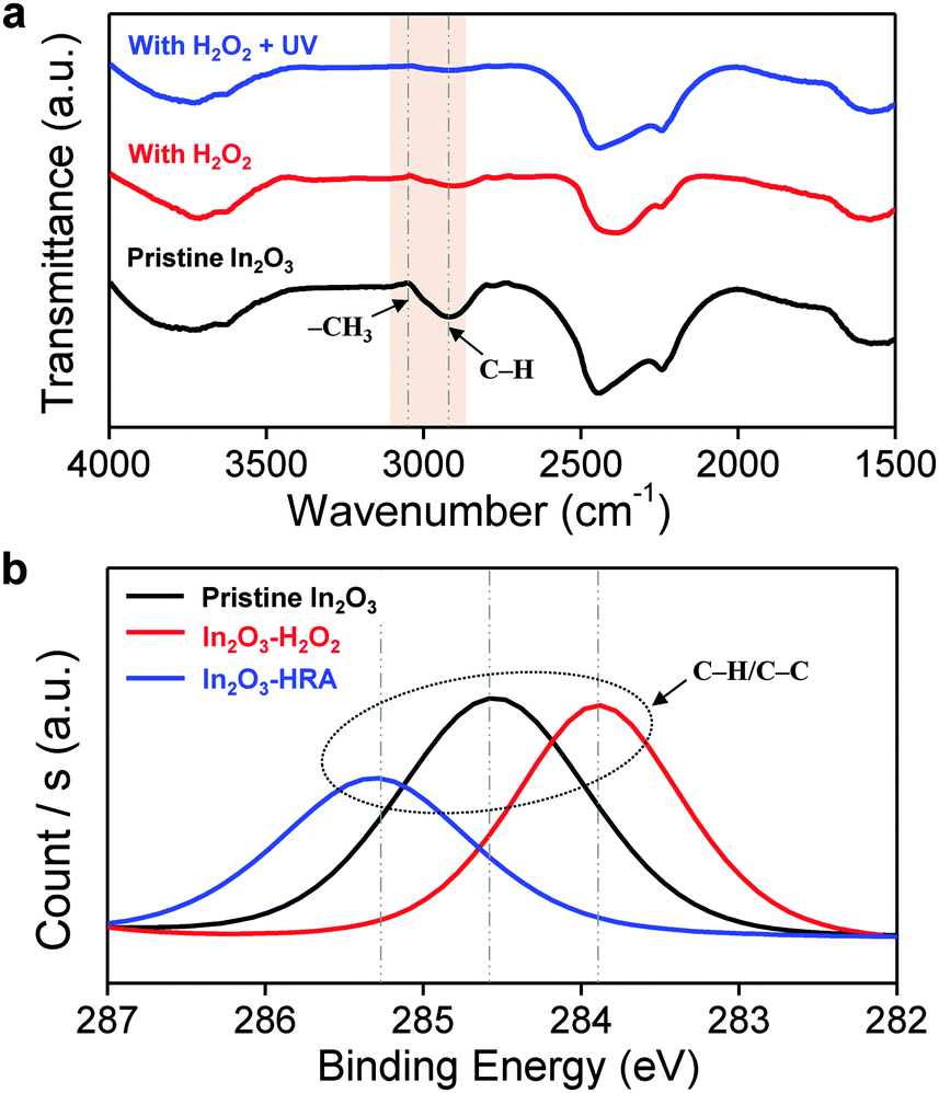
In general, the trap sites in solution-processed oxide TFTs are intimately related to defects that inherently exist in the metal oxide channel layer. These defects include impurities and oxygen deficiencies. The presence of carbon impurities is inevitable because of the organic nature of the solvent. It is important to eliminate organic molecules to the highest possible degree because they can trap electrons, and are therefore detrimental to device operation.24 In this regard, the reduction of carbon impurities in the In2O3–HRA film was confirmed by FTIR (Fig. 3a) and XPS (Fig. 3b). In Fig. 3a, the C–H peak in the range 2950–2900 cm−1 and the CH3 peak in the range 3100–3000 cm−1 were absent.25,26 The absence of these bands implies a pronounced elimination of carbon impurities in the thin film. Similarly, in the C 1s spectra (Fig. 3b), the characteristic peak corresponding to the C–H/C–C peak (∼285 ± 0.6 eV) shows the lowest concentration for the In2O3–HRA film.27 Furthermore, the total atomic ratio for carbon summarized in Fig. 5a indicates that impurities were reduced from 21.86% to 16.64% for the HRA method. These results verify the reduction of carbon impurities in the final HRA thin film.
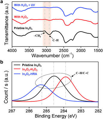 |
| | Fig. 3 Profile of (a) FTIR spectra and (b) XPS C 1s spectra of pristine In2O3, In2O3–H2O2, and In2O3–HRA films. | |
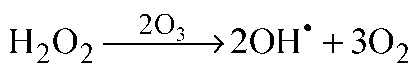
The XPS O 1s peaks of pristine In2O3, In2O3–H2O2, and In2O3–HRA TFTs are shown in Fig. 4. The O 1s peaks are deconvoluted to 530.7 eV (green lines), 531.8 eV (blue lines), and 532.9 eV (orange lines) denoting oxygen bonded to metals (M–O), oxygen deficiencies (Vo), and surface hydroxyl species (M–OH) respectively.28,29 The HRA In2O3 films exhibit a lower degree of hydroxyl species, as expected, despite an increase in oxygen deficiencies. As hydroxide lattices are less efficient in transporting carriers due to broken short intercation distances, it is desirable to reduce M–OH to the lowest possible degree. For In2O3, formation energy of Vo is reportedly lower than that of M–O.13 In the HRA method, molecular oxygen was also produced (eqn (4)) in addition to OH˙ owing to ozone formation. Moreover, decomposition of H2O2 through homolysis (eqn (5)) also yielded molecular oxygen.
| |  | (4) |
Therefore incorporation of oxygen through the HRA method elevated the oxygen content in the lattice as expected. This relationship between oxygen supply and oxygen deficiency formation energy implies that the increase of
Vo observed is due to the additional oxygen supply and not due to defect creation. The quantitative analyses by XPS verify this incorporation of oxygen, showing an increase in the total atomic ratios of oxygen in
Fig. 5b.
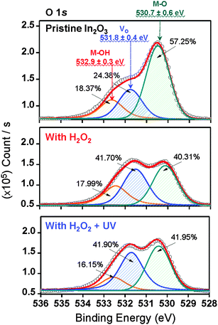 |
| | Fig. 4 Representative XPS O 1s peaks for pristine In2O3, In2O3–H2O2, and In2O3–HRA TFTs. The peaks were fitted representing metal hydroxides (M–OH; 532.9 ± 0.3 eV), oxygen deficiencies (Vo; 531.8 ± 0.4 eV), and metal oxides (M–O; 530.7 ± 0.6 eV). | |
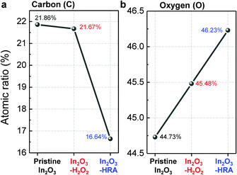 |
| | Fig. 5 Summarized atomic ratio of (a) carbon and (b) oxygen. | |
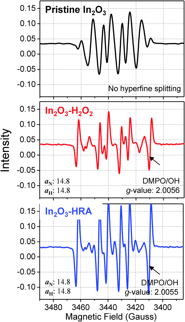
As a simple method that enables both improved mobility and bias stability of In2O3 TFTs, we introduced OH˙ during the film formation process by adding and activating H2O2. The formation of OH˙ was confirmed by ESR spectroscopy (Fig. 6) using a spin trap agent, 5,5-dimethyl-1-pyrroline N-oxide (DMPO). The use of a spin trap agent was necessary due to the transient and short-lived nature of the radicals.30 In Fig. 6, the intensity of DMPO/OH spectra of the In2O3–HRA film was superior to that of In2O3–H2O2. The DMPO/OH spectra are characterized by g-factors of 2.0056 (In2O3–H2O2) and 2.0055 (In2O3–HRA), splitting by one 14N nucleus (aN = 14.8 G) and one 1H nucleus (aH = 14.8 G), respectively.31 This result verify that UV illumination is critical to generate a significant amount of OH˙, as expected in eqn (1). The incorporation of OH˙ into In2O3 synthesis is advantageous for the following two reasons.
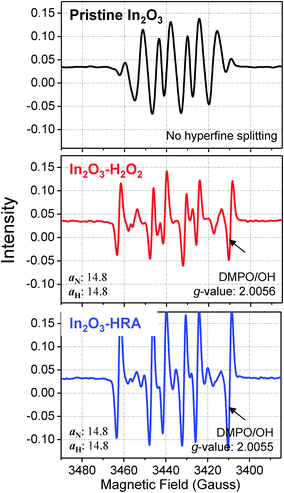 |
| | Fig. 6 ESR spectra of hydroxyl radicals as detected by the DMPO/OH adduct. | |
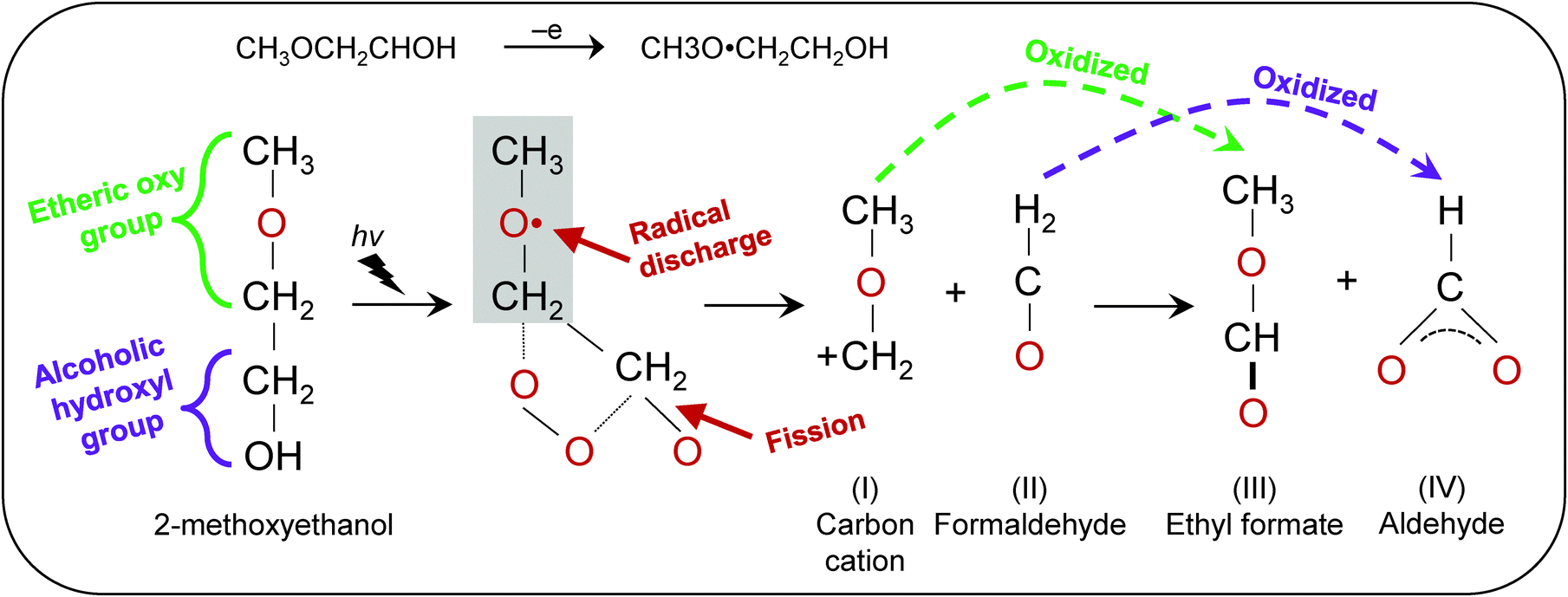
(i) OH˙ as a decomposition agent
The generation of OH˙ in a precursor solution is capable of breaking down organic substrates into smaller molecules. Fig. 7 shows the proposed reaction scheme of HRA decomposition and oxidation. Because organic molecules in the precursor solution primarily originate from the solvent, it is therefore important to focus on the chemical composition of 2-methoxyethanol. Such alkoxyethanols possess two functional groups: (1) alcoholic hydroxyl (–OH) and (2) etheric oxy (–O–) groups.32 Ross and co-workers suggested that oxidation in 2-methoxyethanol occurs through electron transfer at the etheric oxy group rather than the hydroxyl group.33 Upon generation of OH˙ from H2O2, the unpaired electron from OH˙ is discharged at the etheric oxygen which is followed by fission of the C–C and/or C–H bonds between the oxygen atoms. Subsequently, the chain is further degraded leading to the cleavage of –O–CH2–CH2. The reaction produces cation I and formaldehyde II. Then cation I and formaldehyde II are oxidized to yield ethyl formate III and aldehyde IV respectively.34 These smaller molecules can be effectively evaporated, resulting in reduced impurities. The specifics of electron transfer are challenging, but the products obtained indicate that the overall process, probably occurring in a series of steps, is one in which OH˙ oxidizes etheric oxygen and breaks down the methyl group into smaller formaldehyde. With more OH˙ available for transfer of electrons to the etheric oxy group,33 ultimately oxidizing a carbon atom, a significant decrease in carboxylic groups was observed in the end film.
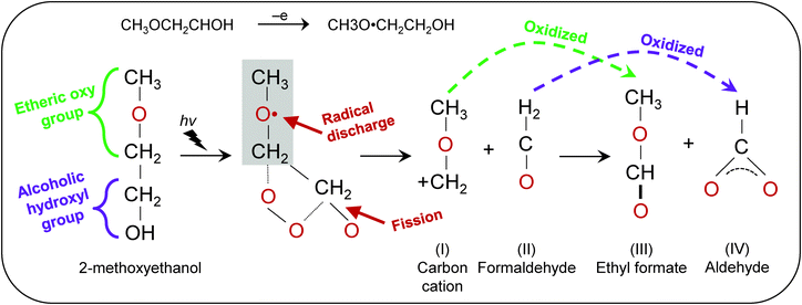 |
| | Fig. 7 Proposed reaction scheme of the hydroxyl radical-assisted decomposition of solution with 2-methoxyethanol solvent. | |
(ii) OH˙ as an oxidizing agent
OH˙ can oxidize sub-gap states from a near conduction band minimum (CBM) state to shallow states, shown in Fig. 8. In amorphous oxides, the states can be located above the valence band maximum (VBM, near-VBM) and below the CBM (near-VBM).35 In the near-VBM state, the localized states are reportedly occupied by electron-acceptors which consist of oxygen sites and low valence cations (In3+ from In 4d and 5s).13 In the near-CBM state, on the other hand, the band consists of electron-donors. The donor-type states are occupied at a neutral charge and can provide electrons by ionization. Fig. 8 shows the schematic illustrations of HRA oxidation that converts neutral near-CBM states to shallow states. It is commonly accepted that Vo in In2O3 are donors, owing to the high density of oxygen sites very close to and just below the CBM.35 In the neutral charge state, Vo in the near-CBM states exhibit inward relaxation by binding two electrons. For In2O3–H2O2, the incorporation of H2O2 is expected to induce states located near-VBM, which are electron acceptors. In contrast, for In2O3–HRA, the incorporation of high density OH˙ is expected to chemically ionize the neutral Vo to give rise to the singly ionized state (Vo+) and the doubly ionized state (Vo++) due to its strong oxidation potential.21 Both of the ionized states are metastable because they are located above the CBM, and are therefore capable of both trapping and donating electrons.36 For the In2O3–HRA TFT, our results indicate that electron donor behavior is more dominant for these metastable states.
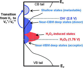 |
| | Fig. 8 Schematic illustrations of the hydroxyl-radical assisted oxidation inducing metastable states. | |
Conclusions
In summary, we have demonstrated In2O3 TFTs exhibiting improved mobility and bias stabilities via a hydroxyl radical-assisted decomposition and oxidation approach. In the thin film formation, hydroxyl radicals reduce carbon impurities and induce the formation of metastable states. In addition, the low annealing temperature that was demonstrated indicates potential for manipulating oxidizing agents in pursuit of low-temperature and high-performance solution-based flexible oxide electronics at low manufacturing cost.
Acknowledgements
This work was supported by (1) the Industrial Strategic Technology Development Program (10041808, Synthesis of Oxide Semiconductor and Insulator Ink Materials & Process Development for Printed Backplane of Flexible Displays Processed below 150 °C) funded by the Ministry of Knowledge Economy (MKE, Korea), and (2) the National Research Foundation of Korea (NRF) grant funded by the Korea government (MSIP) (No. 2011-0028819). We thank Dr M. Shahbuddin of the Kroto Research Institute, University of Sheffield, Sheffield, UK for insightful discussions on organic substrates and FTIR.
References
- E. Fortunato, P. Barquinha and R. Martins, Adv. Mater., 2012, 24, 2945–2986 CrossRef CAS PubMed.
- K. Nomura, H. Ohta, A. Takagi, T. Kamiya, M. Hirano and H. Hosono, Nature, 2004, 432, 488–492 CrossRef CAS PubMed.
- P. Barquinha, L. Pereira, G. Goncalves, R. Martins and E. Fortunato, J. Electrochem. Soc., 2009, 156, H161–H168 CrossRef CAS PubMed.
- S. J. Heo, D. H. Yoon, T. S. Jung and H. J. Kim, J. Inf. Disp., 2013, 14, 79–87 CrossRef CAS PubMed.
- S. J. Kim, S. Yoon and H. J. Kim, Jpn. J. Appl. Phys., 2014, 53, 02BA02 CrossRef.
- H. Nakazawa, Y. Ito, E. Matsumoto, K. Adachi, N. Aoki and Y. Ochiai, J. Appl. Phys., 2006, 100, 093706 CrossRef PubMed.
- H. S. Kim, P. D. Byrne, A. Facchetti and T. J. Marks, J. Am. Chem. Soc., 2008, 130, 12580–12581 CrossRef CAS PubMed.
- M.-G. Kim, M. G. Kanatzidis, A. Facchetti and T. J. Marks, Nat. Mater., 2011, 10, 382–388 CrossRef CAS PubMed.
- S.-Y. Han, G. S. Herman and C.-h. Chang, J. Am. Chem. Soc., 2011, 133, 5166–5169 CrossRef CAS PubMed.
- L. Petti, H. Faber, N. Münzenrieder, G. Cantarella, P. A. Patsalas, G. Tröster and T. D. Anthopoulos, Appl. Phys. Lett., 2015, 106, 092105 CrossRef PubMed.
- H. Faber, Y.-H. Lin, S. R. Thomas, K. Zhao, N. Pliatsikas, M. A. McLachlan, A. Amassian, P. A. Patsalas and T. D. Anthopoulos, ACS Appl. Mater. Interfaces, 2015, 7, 782–790 CAS.
- C.-H. Choi, S.-Y. Han, Y.-W. Su, Z. Fang, L.-Y. Lin, C.-C. Cheng and C.-h. Chang, J. Mater. Chem. C, 2015, 3, 854–860 RSC.
- A. Murat and J. E. Medvedeva, Phys. Rev. B: Condens. Matter Mater. Phys., 2012, 86, 085123 CrossRef.
- N. Mitoma, S. Aikawa, W. Ou-Yang, X. Gao, T. Kizu, M.-F. Lin, A. Fujiwara, T. Nabatame and K. Tsukagoshi, Appl. Phys. Lett., 2015, 106, 042106 CrossRef PubMed.
- M.-F. Lin, X. Gao, N. Mitoma, T. Kizu, W. Ou-Yang, S. Aikawa, T. Nabatame and K. Tsukagoshi, AIP Adv., 2015, 5, 017116 CrossRef PubMed.
- J. M. Kwon, J. Jung, Y. S. Rim, D. L. Kim and H. J. Kim, ACS Appl. Mater. Interfaces, 2014, 6, 3371–3377 CAS.
- M. Danilczuk, F. D. Coms and S. Schlick, J. Phys. Chem. B, 2009, 113, 8031–8042 CrossRef CAS PubMed.
- A. Bosnjakovic and S. Schlick, J. Phys. Chem. B, 2004, 108, 4332–4337 CrossRef CAS.
- J. R. Harbour, V. Chow and J. R. Bolton, Can. J. Chem., 1974, 52, 3549–3553 CrossRef CAS.
- L. Ghassemzadeh, T. J. Peckham, T. Weissbach, X. Luo and S. Holdcroft, J. Am. Chem. Soc., 2013, 135, 15923–15932 CrossRef CAS PubMed.
-
C. W. Jones, Applications of Hydrogen Peroxide and Derivatives, Royal Society of Chemistry, 1999 Search PubMed.
- M. E. Lopes, H. L. Gomes, M. C. R. Medeiros, P. Barquinha, L. Pereira, E. Fortunato, R. Martins and I. Ferreira, Appl. Phys. Lett., 2009, 95, 063502 CrossRef PubMed.
- T.-C. Chen, T.-C. Chang, T.-Y. Hsieh, W.-S. Lu, F.-Y. Jian, C.-T. Tsai, S.-Y. Huang and C.-S. Lin, Appl. Phys. Lett., 2011, 99, 022104 CrossRef PubMed.
- N. Fukuda, Y. Watanabe, S. Uemura, Y. Yoshida, T. Nakamura and H. Ushijima, J. Mater. Chem. C, 2014, 2, 2448–2454 RSC.
-
D. W. Mayo, F. A. Miller, R. W. Hannah and R. Wesley, Course Notes on The Interpretation of Infrared and Raman Spectra, Wiley Online Library, 2004 Search PubMed.
-
K. Nakanishi and P. H. Solomon, Infrared Absorption Spectroscopy, Holden-Day, 1977 Search PubMed.
- X. Deng, A. Verdaguer, T. Herranz, C. Weis, H. Bluhm and M. Salmeron, Langmuir, 2008, 24, 9474–9478 CrossRef CAS PubMed.
- C. Donley, D. Dunphy, D. Paine, C. Carter, K. Nebesny, P. Lee, D. Alloway and N. R. Armstrong, Langmuir, 2002, 18, 450–457 CrossRef CAS.
- Y. J. Tak, D. H. Yoon, S. Yoon, U. H. Choi, M. M. Sabri, B. D. Ahn and H. J. Kim, ACS Appl. Mater. Interfaces, 2014, 6, 6399–6405 CAS.
- C. Lagercrantz, J. Phys. Chem., 1971, 75, 3466–3475 CrossRef CAS.
- K. Makino, T. Hagiwara and A. Murakami, Int. J. Radiat. Appl. Instrum., Part C, 1991, 37, 657–665 CAS.
- B. Das and D. K. Hazra, J. Phys. Chem., 1995, 99, 269–273 CrossRef CAS.
- S. D. Ross, J. E. Barry, M. Finkelstein and E. J. Rudd, J. Am. Chem. Soc., 1973, 95, 2193–2198 CrossRef CAS.
- S. Yamagata, R. Baba and A. Fujishima, Bull. Chem. Soc. Jpn., 1989, 62, 1004–1010 CrossRef CAS.
- K. Nomura, T. Kamiya, E. Ikenaga, H. Yanagi, K. Kobayashi and H. Hosono, J. Appl. Phys., 2011, 109, 073726 CrossRef PubMed.
- H.-K. Noh, K. Chang, B. Ryu and W.-J. Lee, Phys. Rev. B: Condens. Matter Mater. Phys., 2011, 84, 115205 CrossRef.
|
| This journal is © The Royal Society of Chemistry 2015 |
Click here to see how this site uses Cookies. View our privacy policy here. 
 Open Access Article
 This Open Access Article is licensed under a Creative Commons Attribution-Non Commercial 3.0 Unported Licence