
 Open Access Article
 This Open Access Article is licensed under a
 Creative Commons Attribution 3.0 Unported Licence
Fabrication of periodic nanoparticle clusters using a soft lithographic template†
Dae Seok Kima,
Apiradee Honglawanb,
Kyungnam Kimc,
Mun Ho Kimd,
Sohee Jeongce,
Shu Yangbf and
Dong Ki Yoon*a
aGraduate School of Nanoscience and Technology and KINC, KAIST, Daejeon 305-701, Republic of Korea. E-mail: nandk@kaist.ac.kr
bDepartment of Chemical and Biomolecular Engineering, University of Pennsylvania, PA 19104, USA
cNanomechanical Systems Research Division, Korea Institute of Machinery and Materials, Daejeon, 305-343, Republic of Korea
dDepartment of Polymer Engineering, Pukyong National University, Pusan, 608-739, Republic of Korea
eDepartment of Nano Mechatronics, University of Science and Technology, Daejeon, 305-350, Republic of Korea
fDepartment of Materials Science & Engineering, University of Pennsylvania, 3231 Walnut Street, PA 19104, USA
First published on 8th April 2015
Abstract
A novel fabrication method has been developed for the preparation of a periodic array of nanoparticle clusters (NPCs) using a sublimable liquid crystal (LC) material. The defect structures of the LC film provide the specific topographical confinement to trap nanoparticles (NPs) and assemble the NPs to generate NPCs during thermal annealing. This system shows a simple regulation of the size of NPCs by varying the concentration of the NP-suspension. Additionally, an illumination system using quantum dots (QDs) is fabricated using the manipulation method reported here.
NPs that self-assemble into ordered nanostructures present unusual structural and opto-electric characteristics.1–3 Especially, the creation of a large area array of NPCs is one of the most important interdisciplinary topics in current materials science and optoelectronics for the manipulation of tuneable photonic devices. To date, many assembling methods, including drying oil-emulsion template in water, electrostatic assembly, chemical vapour deposition and template assisted assembly, have been tried to control the ordering and orientation of NPCs.3–6 However, achieving a well-ordered array of NPCs is still a complex and expensive process.7,8 One of the promising methods used in the assembly of NPs is the self-organization process in a LC medium.9 Herein, we demonstrate the fabrication of a periodic array of NPCs over a large area using a sublimable LC material. This is mainly governed by two factors: the topographical LC dimpled structures to confine the NPs and the sublimation–reconstruction phenomenon of small molecular weight LC molecules to generate a NPC array. The number of NPs in a NPC, which is important for the optoelectronic properties, is controlled by varying the concentration of the NP suspension. We extend the method to create a hexagonal array of QDs for a fluorescent display, where the symmetry of the clusters is determined by a highly periodic defect array of toric focal conic domains (TFCDs). We believe that the toolkit presented here is universal and will find uses in other new applications involving the assembly of NPs or NPCs.
Highly periodic dimpled structures, the TFCDs of the smectic A LC phase (SmA), are formed by the antagonistic surface anchoring, planar anchoring on the solid substrate and homeotropic anchoring at the air/LC interface.10 It was shown that TFCDs can be used as lithographic tools to address particles in the line defect of the dimple sites.9 However, after the assembly of particles, LCs remain in the matrix. For many practical applications, it will be desirable to remove the assembling LCs. It has been shown that like ice in winter, the small molecular weight LC molecules exhibit the sublimation and reconstruction properties that enable the TFCDs at the micron scale to transform into dome-like TFCDs with hemicylinders at the nanometre scale during the thermal annealing process.11,12
To create the NPC array using a sublimable LC material, we first prepare a rod-type semifluorinated LC molecule, Y002 (Fig. 1a),10 which undergoes transitions from the isotropic state to the SmA phase, the smectic E phase (SmE) and to the crystalline phase from 195 °C to room temperature and has thermal sublimation properties.11,12 As a proof-of-concept, we also synthesized multidimensional NPs, including fluorinated silica NPs (F-SiO2; diameter (d) ∼ 100 nm) and QDs (CdSe/CdS/ZnS, 4–5 nm in diameter) according to the literature.13,14 As illustrated in Fig. 1b to g, the powder sample, Y002, is first placed on a clean Si(100) wafer with planar anchoring, followed by heating up to the isotropic temperature to spread the LC sample with a thickness of ∼10 μm.‡ After cooling to room temperature, TFCDs with dimpled structures are spontaneously generated on top, typically a few μm in width and hundreds of nanometers in depth, which can be varied by the LC film thickness.15 These topographical dimples can grab or confine the particles similar to the photo-lithographically generated hole patterns.6 To use these dimpled structures as a template for the NPC arrays, a 0.01 wt% suspension of F-SiO2 NP in a Novec 7300 (3 M) is spin coated (2000 rpm, 15 s) on the TFCD film (Fig. 1e). As the sample is dried via solvent evaporation, the NPs aggregate irregularly at each dimple site (Fig. 1f). When annealed at 160 °C, the smectic layers of TFCDs are slowly removed layer by layer as a function of time. In particular, the layers near the dimpled region sublime slower than other sites and become spherically reoriented with F-SiO2 NPs at the same time. Finally, a hexagonal array of NPCs is generated (Fig. 1g) after 4 h of thermal annealing. This fabrication process is directly investigated using depolarized reflected light microscopy (DRLM) and scanning electron microscopy (SEM). Despite the existence of a layer of F-SiO2 NPs on top, the hexagonal array of TFCDs shows typical Maltese cross-patterns in the DRLM images at room temperature (Fig. 2a), indicating that the molecular director is radially orientated at the bottom of the substrate. The corresponding SEM image confirms that the micron-scale TFCDs are not distorted by NPs (Fig. 3a).‡
 | ||
| Fig. 1 Liquid crystal materials and schematic representation of the strategy used to fabricate NPC arrays. (a) The structures, phases, and transition temperatures of the rod type LC material, Y002 (all temperatures are in degrees of Celsius). (b) A clean pristine Si(100) wafer is prepared. (c) Y002 is placed on the Si wafer and then heated above the isotropic temperature (∼200 °C). (d) TFCD array is formed upon cooling from the isotropic state to SmA (∼160 °C). (e) The NP suspension is spread and spin-coated on the TFCD array. (f) NPs are spontaneously aggregated at the dimple region of the TFCD array. (g) NPC arrays are generated with hexagonal symmetry after thermal annealing for 4 h. | ||
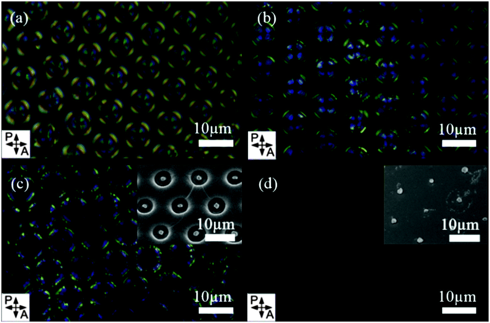 | ||
| Fig. 2 DRLM with cross-polarizers and SEM images of the TFCDs top-coated by F-SiO2 NPs during thermal annealing at 160 °C. (a) The initial state of the TFCDs showing Maltese cross patterns. (b, c) The images of TFCDs are taken after 1 and 2 h annealing, respectively. The molecular arrangement at the micron scale does not change compared to the initial state. (d) The totally dark image is observed after all the LC molecules were removed by sublimation. The insets of (c, d) are the corresponding SEM images, respectively. | ||
 | ||
| Fig. 3 SEM images and the corresponding illustrations of the NPCs during thermal annealing. (a) SEM image of the initial state showing the relatively flat arrangement of F-SiO2 particles on the TFCD. (b, c) As time goes by, at ∼160 °C smectic LC layers are sublimed and partially reconstructed to spherically address NPs at the dimple region of the TFCD. (d) NPs remain at the dimple position of the TFCD after all the LC materials are sublimed. A series of illustrations show that the layers of the dimple region are mixed with NPs, whereas the interconnecting layers between dimples were gradually removed during thermal annealing. Finally, the NPs accumulate together to form a NPC on the substrate without the LC material. The wider arrow means the faster subliming rate in (b, c). | ||
After heating and dwelling of the sample at 160 °C for 1 h, the LC molecules are slowly sublimed from the top-surface of the sample, gathering NPs, thus forming a NPC in the dimple region (Fig. 3b). This selective gathering behaviour is consistent with the characteristics of the sublimable LC molecules, which sublimed much slower (indicated by thin and thick arrows in Fig. 3b and c) in the dimpled regions than at the peripheral area of the dimple, as illustrated in Fig. 3b and c. The different sublimation rates in the dimple and the other areas of the TFCD are resulted from a combined effect of surface tension and surface orientational interactions.11 As the thermal annealing proceeds, more air/LC interface is exposed to induce the homeotropic alignment of LC molecules, which means that the smectic layers are aligned in parallel with the air/LC interface. In this process, the antagonistic alignment of LC molecules in the line defect, the dimple site and the other places of the TFCD forms a dome-like structure because the molecules in the line defect have a greater resistance to the thermal sublimation compared to the edge of the TFCD.11 This interesting behaviour reveals differently when the F-SiO2 NPs are placed on top of the TFCD.
The macroscopic reorientation of LC molecules is not seen although the NPs migrate to the top-surface of TFCDs during the thermal annealing (Fig. 2b and c). This is due to the small elastic energy of the TFCD, which does not overcome the surface energy that can reorient LC molecules to satisfy the planar anchoring of NPs at the LC/air interface.16 A few hundreds of nm-sized concentric ring-patterns are generated, as the total thickness of TFCDs is gradually reduced with increasing thermal annealing time at the SmA phase (160 °C) for ∼2 h (Fig. 3c).11,12 Topographically, the centre of the ring patterns becomes higher while the surroundings are sublimed away, resulting in a NPC protrusion in the centre of the ring-patterns (Fig. 3c). Most of the NPs are gathered at the dimple site of the TFCD to form a NPC (Fig. 3c), showing a diameter of ∼2 μm in the hexagonal array (insets of Fig. 2c and 3c). After a 4 h thermal annealing process, all the LC materials are gone, leaving only the spherical aggregates of F-SiO2 NPs at the original dimple site of the TFCD (Fig. 3d). This is also observed in the DRLM image, showing no birefringence (Fig. 2d), indicating the complete removal of the LC molecules. The size of the NPC is reduced to ∼800 nm, and the SEM image clearly shows a highly-ordered NPC array (insets of Fig. 2d and 3d) over a large area (∼500 × 500 μm2).
The roles of F-SiO2 NPs relevant to the clustering of NPs are as follows: (i) spreading of NPs on the TFCDs reduces the sublimating rate of the LC material especially at the dimpled region as shown in Fig. 3b and c. The more NPs are gathered in the dimpled region with increasing thermal annealing time, which hinder the direct contact of LCs with the air boundary, the less LC molecules being removed in this area. As a consequence, the LC molecules in the peripheral region of TFCDs without NPs sublime much faster where molecules are vertically aligned. (ii) Top-coated NPs locally induce planar anchoring to Y002 molecules,16 leading to the intercalation of LC molecules among the NPs to form a spherical NPC during the thermal annealing. Supporting this is the reduced NPC size from ∼2 μm (2 h) to ∼800 nm (4 h) as shown in Fig. 3c and d, respectively.
We then investigated a control of the NPC size by varying the concentration of the NP-suspension (Fig. 4). As the concentration varies from 0.001 wt% to 0.5 wt%, the size of the NPC also varies from 400 nm to 1.8 μm in diameter, meaning that the number of NPs in a cluster might be commensurate from ∼64 to ∼6000. At a concentration as low as 0.0001 wt%, we observe a single or dimer form of NPs, meaning that our building block, F-SiO2 NP, has a critical size forming NPC around this concentration. In contrast, at 1 wt% suspension, relatively irregular NPCs are obtained and NPs are not well-gathered in the dimpled region of TFCDs. Instead, they spread over the substrate after thermal annealing. This tendency can be also found in NPCs made from 0.5 wt% suspension, showing the irregular aggregation in the background (Fig. 4f). The clustering of NPs shown in Fig. 4g can be qualitatively understood by a simple growth pattern.7 This size tenability is very important for the photonic and optoelectronic applications,17,18 where the optoelectronic properties of each NPC can be varied with the degree of aggregation of NPs.
 | ||
| Fig. 4 SEM images of NPCs with varied concentrations of the NP suspensions and their relationship. A series of SEM images of the NPC using varied concentrated suspension of NPs of (a) 0.001 wt%, (b) 0.005 wt%, (c) 0.01 wt%, (d) 0.05 wt%, (e) 0.1 wt%, and (f) 0.5 wt%. (g) The plot quantitatively shows an increase in the size of the NPCs as a function of concentration of NP suspension. In this plot, the x-axis, concentration is a log-scale, while the y-axis is the diameter of NCPs. | ||
To demonstrate the versatility of our method, we extend the study to manipulate the illumination from QDs. The semiconductor QDs present size-tuneable optical properties arising from the quantum confinement effects, which are very attractive for display devices.19,20 There have been many studies to fabricate a QD array, including the dewetting method using a mold, inkjet printing, solution-based nucleation and growth and transfer printing.21–24
Nevertheless, it often requires pre-patterning of the templates, the use of expensive equipment, and complex processing steps. Here, in order to realize the illumination, we only need sublimable LC materials and CdSe/CdS/ZnS QDs with an excitation maximum at ∼450 nm (blue) and emission at ∼550 nm (green). As shown in the fluorescent microscopy image (Fig. 5), a hexagonal array of QD clusters is observed over a large area (∼500 × 500 μm2) in ∼4 h via the spontaneous assembly of QDs and LCs. The fast Fourier transform (FFT) (inset in Fig. 5) clearly shows the well-ordered QD cluster arrays in a hexagonal symmetry. Moreover, it is possible to realize various types of arrays of NPCs including QD-clusters by using the topographical confinement of LCs.10,25–28
 | ||
| Fig. 5 The QD clusters based illumination. A fluorescent microscopy image of the QD clusters in the hexagonal array. Inset is 2 dimensional fast Fourier transform. | ||
Conclusions
We have developed a simple method to fabricate a periodic array of NPCs using sublimable LCs. This process is mainly governed by the thermal annealing conditions to control the sublimation rate and the reconstruction phenomenon of sublimable LCs. The dimples of TFCDs provide important topographical sites to trap and assemble NPs to form NPCs during the thermal annealing. The NPs in turn slow down the sublimation of LCs in the dimpled regions. We also show that the size of the NPCs can be conveniently controlled by varying the concentration of the NP-suspension. As a proof-of-concept, an illumination system consisting of a hexagonal array of QDs is fabricated. The self-assembly approach demonstrated here can be applied to a flexible substrate and will offer a new universal platform to fabricate and explore optoelectronic devices via bottom-up approaches.Acknowledgements
This study was supported by the grant from the National Research Foundation (NRF), funded by the Korean Government (2014M3C1A3052537, 2012M3A7B4049802, 2014S1A2A2027911, and 2014M1A8A1049303). S.Y. and A.H. acknowledge support from the National Science Foundation (NSF) MRSEC grant, DMR1120901. K. K and S. J. were partially supported by the Basic Research Fund from KIMM.Notes and references
- S. M. Spillane, T. J. Kippenberg and K. J. Vahala, Nature, 2002, 415, 621 CrossRef PubMed.
- J. A. Fan, C. Wu, K. Bao, J. Bao, R. Bardhan, N. J. Halas, V. N. Manoharan, P. Nordlader, G. Shvets and F. Capasso, Science, 2010, 328, 1135 CrossRef PubMed.
- J. Lacava, P. Born and T. Kraus, Nano Lett., 2012, 12, 3279 CrossRef PubMed.
- F. L. Yap, P. Thoniyot, S. Krishnan and S. Krishnamoorthy, ACS Nano, 2012, 6, 2056 CrossRef PubMed.
- A. Valsesia, P. Colpo, T. Meziani, F. Bretagnol, M. Lejeune, F. Rossi, A. Bouma and M. G. Parajo, Adv. Funct. Mater., 2006, 16, 1242 CrossRef PubMed.
- Y. Xia, Y. Yin, Y. Lu and J. McLellan, Adv. Funct. Mater., 2003, 13, 907 CrossRef PubMed.
- B. Yan, A. Yhubagere, W. R. Premasiri, L. D. Ziegler, L. D. Negro and B. M. Reinhard, ACS Nano, 2009, 3, 1190 CrossRef PubMed.
- L. Gunnarsson, J. E. Bjerneld, H. Xu, S. Petronis, B. Kasemo and M. Kall, Appl. Phys. Lett., 2001, 78, 802 CrossRef PubMed.
- C. Blanc, D. Coursault and E. Lacaze, Liq. Cryst. Rev., 2013, 1, 83 CrossRef.
- D. K. Yoon, M. C. Choi, Y. H. Kim, M. W. Kim, O. D. Lavrentovich and H. T. Jung, Nat. Mater., 2007, 6, 866 CrossRef PubMed.
- D. K. Yoon, Y. H. Kim, D. S. Kim, O. S. Oh, I. I. Smalyukh, N. A. Clark and H. T. Jung, Proc. Natl. Acad. Sci. U. S. A., 2013, 110, 19263 CrossRef PubMed.
- D. S. Kim, Y. J. Cha, H. Kim, M. H. Kim, Y. H. Kim and D. K. Yoon, RSC Adv., 2014, 4, 26946 RSC.
- L. Xu, R. G. Karunakara, J. Guo and S. Yang, ACS Appl. Mater. Interfaces, 2012, 4, 1118 Search PubMed.
- K. Kim, J. Y. Woo, S. Jeong and C. S. Han, Adv. Mater., 2011, 23, 911 CrossRef PubMed.
- Y. H. Kim, D. K. Yoon, M. C. Choi, H. S. Jeong, M. W. Kim, O. D. Lavrentovich and H. T. Jung, Langmuir, 2009, 25, 1685 CrossRef PubMed.
- D. A. Beller, M. A. Gharbi, A. Honglawan, K. J. Stebe, S. Yang and R. D. Kamien, Phys. Rev. X, 2013, 3, 041026 Search PubMed.
- F. Kretschmer, F. Kretschmer, M. Fruhnert, R. Geiss, U. Mansfeld, C. Hoppener, S. Hoeppener, C. Rockstuhl, T. Pertsch and U. S. Schubert, J. Mater. Chem. C, 2014, 2, 6415 RSC.
- R. Philip, P. Chantharasupawong, H. Qian, R. Jin and J. Thomas, Nano Lett., 2012, 12, 4661 CrossRef PubMed.
- J. Lim, S. Jun, E. Jang, H. Baik, H. Kim and J. Cho, Adv. Mater., 2007, 19, 1927 CrossRef CAS PubMed.
- E. Jang, S. Jun, H. Jang, J. Lim, B. Kim and Y. Kim, Adv. Mater., 2010, 22, 3076 CrossRef CAS PubMed.
- W. Cheng, N. Park, M. T. Walter, M. R. Hartman and D. Luo, Nat. Nanotechnol., 2008, 3, 682 CrossRef CAS PubMed.
- V. Wood, M. J. Panzer, J. Chen, M. S. Bradley, J. E. Halpert, M. G. Bawendi and V. Bulovic, Adv. Mater., 2009, 21, 2151 CrossRef CAS PubMed.
- C. B. Murray, C. R. Kagan and M. G. Bawendi, Annu. Rev. Mater. Sci., 2000, 30, 545 CrossRef CAS.
- T. H. Kim, C. B. Murray, C. R. Kagan and M. G. Bawendi, Nat. Photonics, 2011, 5, 176 CrossRef CAS.
- A. Honglawan, D. A. Beller, M. Cavallaro, R. D. Kamien, K. J. Stebe and S. Yang, Adv. Mater., 2011, 23, 5519 CrossRef CAS PubMed.
- A. Honglawan, D. A. Beller, M. Cavallaro, R. D. Kamien, K. J. Stebe and S. Yang, Proc. Natl. Acad. Sci. U. S. A., 2013, 110, 34 CrossRef CAS PubMed.
- B. Zappone, C. Meyer, L. Bruno and E. Lacaze, Soft Matter, 2012, 8, 4318 RSC.
- T. Ohzono, Y. Takenaka and J. I. Fukuda, Soft Matter, 2012, 8, 6438 RSC.
Footnotes |
| † Electronic supplementary information (ESI) available. See DOI: 10.1039/c5tc00687b |
| ‡ Materials and procedures: Y002, F-SiO2 NPs (d ∼ 100 nm), and QDs (CdSe/CdS/ZnS, 4–5 nm in diameter) were synthesized as reported previously with some modifications.10,13,14 A Si wafer was cleaned by rinsing with acetone and ethanol to remove organic and inorganic impurities, and then dried by N2 gas. To introduce planar anchoring at the bottom of the substrate, 1 wt% polyethylene imide (Sigma Aldrich) solution was spin-coated on the cleaned Si wafer and baked at 90 °C for 30 min. Then Y002 powder was placed on the substrate and heated to the isotropic temperature (∼200 °C) on a heating stage (LINKAM LTS350) controlled by a temperature controller (LINKAM TMS94), and cooled down to room temperature to form the TFCDs. To form NPCs, F-SiO2 NPs and CdSe/CdS/ZnS QDs were spin coated onto the TFCDs and maintained at 160 °C for 1, 2, and 4 h, respectively, to observe the sequential changes of the clusters. Characterization by DRLM, SEM, and FM: the clustering NPs were directly imaged using a DRLM (LV100POL, Nikon) and a field-emission SEM (FE-SEM, Hitachi, S-4800). The fluorescent image of the QD-cluster array was obtained using a epi-fluorescence microscope (LV-UDM, Nikon). The excitation and emission wavelengths were in the range 440–460 nm and 540–560 nm, respectively. |
| This journal is © The Royal Society of Chemistry 2015 |