
 Open Access Article
 This Open Access Article is licensed under a
 Creative Commons Attribution 3.0 Unported Licence
Optically switchable transistors comprising a hybrid photochromic molecule/n-type organic active layer†
K.
Börjesson
a,
M.
Herder
b,
L.
Grubert
b,
D. T.
Duong
c,
A.
Salleo
c,
S.
Hecht
*b,
E.
Orgiu
*a and
P.
Samorì
*a
aISIS & icFRC, Université de Strasbourg & CNRS, 8 allée Gaspard Monge, 67000 Strasbourg, France. E-mail: samori@unistra.fr; orgiu@unistra.fr
bDepartment of Chemistry, Humboldt-Universität zu Berlin, Brook-Taylor-Str. 2, 12489 Berlin, Germany. E-mail: sh@chemie.hu-berlin.de
cDepartment of Materials Science and Engineering, Stanford University, Stanford, California 94305, USA
First published on 18th March 2015
Abstract
Organic semiconductors can be easily combined with other molecular building blocks in order to fabricate multifunctional devices, in which each component conveys a specific (opto)electronic function. We have fabricated photoswitchable hybrid thin-film transistors based on an active bi-component material, consisting of an n-type fullerene derivative and a photochromic diarylethene that possesses light-tunable energy levels. The devices can be gated in two independent ways by either using an electrical stimulus via the application of a voltage to the gate electrode or an optical stimulus causing interconversion of the diarylethene molecules between their two isomers. Fine control over the device output current is achieved by engineering the diarylethenes' LUMO that can act as an intra-gap state controlled by a distinct wavelength in the UV or in the visible range. Importantly, the devices based on a mixed diarylethene/fullerene active layer preserve the high mobility of the pristine semiconductor.
Introduction
Photochromic molecules are building blocks capable of undergoing reversible isomerization between two (meta)stable states in response to light stimuli. The two isomers possess significantly different physical and chemical properties, making these molecules very attractive as active components for applications in multifunctional devices and logic circuits.1–6 Prototypes of logic gates are realized in solution by proving the reversible processes of write and read relying on irradiation with light at different wavelengths or other chemical stimuli acting on multi-chromophore systems.7–10 In organic electronics the embedded photochromic molecules can exhibit a slightly simpler monochromophore chemical design but their incorporation in the active layer of a device requires control over their structural interactions with the semiconductor and matching of their mutual energy levels. The reward for incorporating a photochromic molecular unit into a standard organic thin-film transistor (TFT) is the integration of a new functionality into an already existing platform, in which the output device current can be simultaneously and independently controlled through light and voltage.Photomodulation of current has been achieved by using neat photochromic molecules,11 synthesizing hybrid molecules consisting of a photochromic system covalently or supramolecularly attached to an organic (semi)conductor,12–19 or by combination of photochromic systems and organic semiconductors in blends or layered devices.20–24 The latter approaches offer the advantage of high switching ratios while maintaining high charge carrier mobilities. Self-assembled monolayers (SAMs) of azobenzenes or diarylethenes (DAEs) have also been used to modulate conductance in two-terminal devices.25–28 Among photochromic molecules, DAEs are potentially best suited for photocontrolling electrical charge transport as their π-electronic structure changes considerably upon isomerization. Furthermore, they combine complete thermal bi-stability with high fatigue resistance to repeated photoisomerization.29–31 Recently, light responsive field-effect transistors have been realized by exploiting similar approaches. Device performances such as field-effect mobility and threshold voltage have been photomodulated either by chemisorption of switchable SAMs or by blending photochromic molecules with the dielectric material.32–35 In order to achieve high switching ratio, Hayakawa et al. used a biphenyl-DAE derivative as the active layer in an organic field-effect transistor (oFET), attaining two orders of magnitude current switching ratio, but in devices exhibiting modest field-effect mobilities of p-type.36
Different groups have recently achieved high switching ratios while maintaining high mobilities by blending a p-type polymer semiconductor with DAEs.37,38 In particular, the switching effect is achieved by tuning of the HOMO levels of the photochromic component in the blend via light irradiation at a selected wavelength. In such a way, one of the two isomers acts as a trap center for holes while the other simply represents a scattering center for charges, without energetic interaction with the active layer. While this principle was anticipated in previous theoretical and computational work,39 to prove its general applicability it would be desirable to apply it also on n-type systems via optical tuning of the LUMO levels.
Herein, we report for the first time the fabrication and characterization of photoswitchable TFTs combining a photochromic system and n-type semiconductors, therefore exploiting the photoisomerization to generate photoswitchable electron-instead of hole-accepting levels. Our findings allowed us to extend the previously proposed switching mechanism to electron transport while comparing the device performances of two different semiconductors incorporating two different photochromic units, giving in total four different binary semiconductor/photochromic molecule blends. As model n-type semiconductors, two solution processable fullerene derivatives were used, i.e. [6,6]-phenyl-C61-butyric acid methyl ester (PCBM) and indene-C60 bisadduct (ICBA).40,41 Both fullerene derivatives exhibit n-type transport when incorporated in TFTs, although their LUMO levels differ slightly (Fig. 1).42,43 Furthermore, two structurally similar yet electronically different DAEs are employed. Both DAEs are functionalized with the strongly electron withdrawing perfluorocyclopentene bridge as well as CF3-substituted phenyl rings on both hetaryl moieties in order to obtain highly electron-deficient structures possessing low LUMO levels. Using thiazoles (DAE-FN) in place of thiophenes (DAE-F) as hetaryl moieties allows for fine-tuning of the electronic levels due to the more electro-negative nitrogens within the π system (see ESI† for synthetic procedures). These functionalizations allow the molecular LUMO energy to be lowered by 1 eV below that of the corresponding non-functionalized DAE. The structure and LUMO levels of all molecules encompassed in our study are portrayed in Fig. 1.
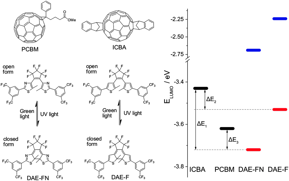 | ||
| Fig. 1 Left: chemical structures of the semiconductors (PCBM and ICBA) and of the two diarylethenes, denoted DAE-FN and DAE-F, in their open and closed forms. Right: LUMO levels determined by cyclic voltammetry of the fullerene derivatives (black), and the diarylethenes in their open (blue) and closed (red) forms. | ||
Results and discussion
Driving force for electron transfer
The two fullerene derivatives and the two diarylethenes can form four different binary semiconductor/photochromic system blends. A driving force for trap formation of electrons exists when the LUMO level of the DAE lies lower than the LUMO of the semiconductor. As displayed by the LUMO levels in Fig. 1 and Table S1 (ESI†), approximated by reduction potentials in cyclic voltammetry (see ESI† for details), the energy difference ΔE1 = 0.29 eV between ICBA and DAE-FNclosed is larger than ΔE2 (ICBA/DAE-Fclosed) and ΔE3 (PCBM/DAE-FNclosed), both being 0.10 eV. Therefore the LUMO of the closed isomer of DAE-FN is lying deeper in the band gap of ICBA than in any of the other binary combinations. ICBA and DAE-F, and PCBM and DAE-FN have the same driving force for trap formation as determined by cyclic voltammetry making it unclear from an energetic point of view which combination represents the deepest trapping level. In the PCBM/DAE-F blend both the closed and open isomer of the photochromic unit have their LUMO lying higher than that of the semiconductor therefore no driving force exists for electrons to sit in such level. Noteworthy, for all combinations the LUMO level of the open DAE form is energetically unfavourable for the charge carriers transported within the semiconductor matrix. Note that the conversion of electrochemical reduction potentials to LUMO levels and the comparison of structurally different compounds can only be an approximation, as the influence of solvation of the derived radical anion and the surrounding in the solid phase is neglected.44 Also chemical reactions following the electron transfer may significantly shift the peak potential. Thus, for the ring-open isomers of DAE-FN and DAE-F, both possessing irreversible reduction waves, the given LUMO energies are only rough estimates, which however show that they are way higher than the LUMO energies of the fullerene derivatives. In contrast, the reductions of both ring-closed isomers possess a quasi-reversible character, i.e. upon slow scan rates they are irreversible while upon higher scan rates they become reversible (Fig. S4, ESI†). Given the similar chemical structures of DAE-FN and DAE-F the comparison of their reduction potentials at high scan rates and derived LUMO levels is valid, showing the significantly higher electron affinity of DAE-FN. The positioning of the DAE's LUMO levels relative to the fullerenes and with this the absolute driving force for electron transfer are somewhat more uncertain, however, using cyclic voltammetry still gives an easy and good prediction of the experimental trends to be expected.Photophysical properties in films and solution
When blending a photochromic molecule together with another light-absorbing component in a solid film, it is important to verify that the photoisomerization ability of the photochromic system is retained. Fig. 2a and b portrays the absorption spectra of both open and closed forms of DAE-FN and DAE-F in acetonitrile solution (see ESI† for spectroscopic details in solution). The closed forms exhibit absorption maxima at 538 and 592 nm for DAE-FN and DAE-F, respectively. Both DAEs can repeatedly be switched between the open and closed isomer without any sign of degradation (see Fig. 2a and b inset) and the photochemical quantum yields are 0.45 and 0.58 for the open → closed photoisomerization as well as 0.04 and 0.02 for the closed → open photoisomerization of DAE-FN and DAE-F, respectively (Table S2, ESI†). The lower quantum yield for the closed → open isomerization, which is a common feature in this type of diarylethenes,29 was compensated in device experiments by longer irradiation times and higher photon fluxes as compared to the open → closed process (vide infra).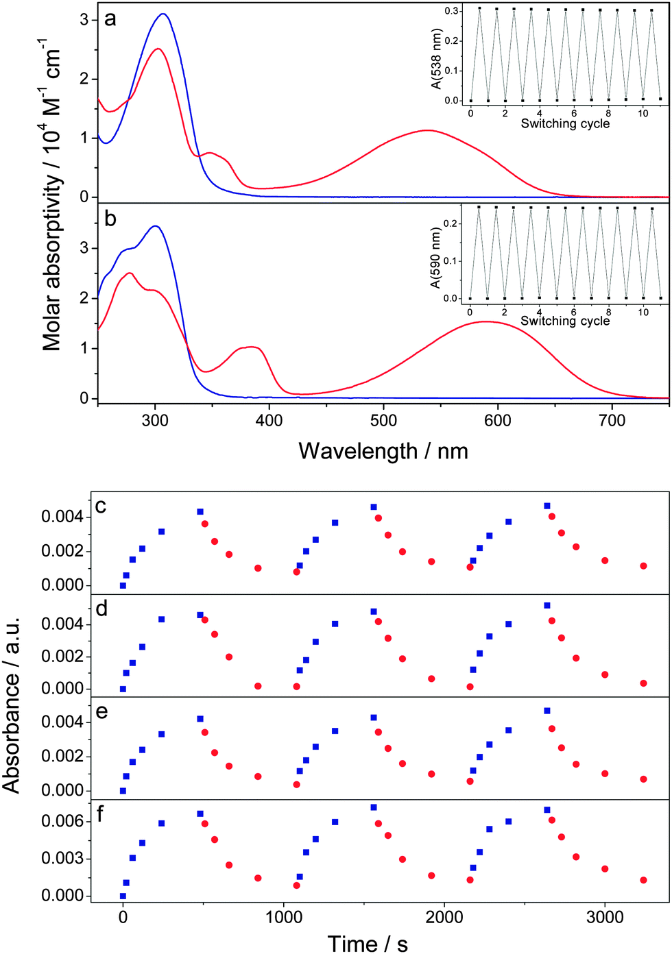 | ||
| Fig. 2 Molar absorptivities of the open (blue line) and closed (red line) isomers of (a) DAE-FN, and (b) DAE-F dissolved in acetonitrile (insets show absorption in the visible range during repetitive switching between the open and closed forms using UV and visible light). Absorbance at 540 nm or 590 nm for DAE-FN and DAE-F blended films on glass substrates as a function of irradiation time for (c) PCBM/DAE-FN blend, (d) PCBM/DAE-F blend, (e) ICBA/DAE-FN blend, and (f) ICBA/DAE-F blend. Irradiation wavelengths were 315 nm (blue squares) or 530 nm (red circles). | ||
The absorption maxima of the lowest energy absorption band of the DAEs in their closed form were used to monitor the switching behavior of the DAEs in blended films together with the fullerenes (Fig. 2c–f). The films were thin enough to allow light to penetrate the films both at the irradiating and monitoring wavelengths. All these films show an increase in their absorption after irradiation with UV light, and a subsequent decrease when irradiated with green light, confirming that the DAEs retain their ability to reversibly photoisomerize in blended films.
Photoswitching of transistors
To explore the closed form of the DAEs' ability to act as an electron acceptor and thus modulate reversibly the electron mobility in semiconductor/DAE blends, thin-film transistors were made by spin coating fullerene/DAE blends (weight ratio = 5 to 1) solubilized in chlorobenzene on SiO2 substrates. The SiO2 substrates were pretreated with HMDS and contained prepatterned 1-undecanethiol treated gold electrodes giving transistors in a bottom-gate bottom-contact configuration. Fig. 3 shows transfer sweeps before and after switching the diarylethenes from their open to their closed form. For all cases the switching either lowers the drain–source current or does not affect transistor performance at all, which is in accordance to expectations since the closed isomer with its lower LUMO level has a higher tendency to act as an electron accepting level than the open isomer. Importantly, switching between the open and closed isomers does not change the threshold voltage of the devices (Fig. S8, ESI†).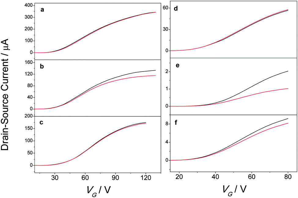 | ||
| Fig. 3 Examples of IDvs. VG sweeps before (black) and after (red) switching from the open to the closed form by irradiation at 320 nm for (a) pristine PCBM, (b) PCBM/DAE-FN blend, (c) PCBM/DAE-F blend, (d) pristine ICBA, (e) ICBA/DAE-FN blend, and (f) ICBA/DAE-F blend. | ||
To further examine the switching properties, the transistors were irradiated with monochromatic light centered at λ = 320 nm or λ = 540 nm in order to induce the open → closed or closed → open photoisomerization, respectively. Fig. 4 shows the normalized drain–source current of TFTs made from the different semiconductor/DAE blends or pristine semiconductor. Transfer curves were acquired in the saturation regime in dark conditions and the current values were recorded at a fixed (VGS–Vth) and VDS voltage for each entry (VGS,ICBA = +80 V, VGS,PCBM = +120 V, VDS = +40 V). The irradiation of the pristine semiconductors with light of different wavelengths led to negligible changes in current, likewise for the PCBM/DAE-F blend. In view of the LUMO levels displayed in Fig. 1, the latter result is not surprising because of the absence of any driving force for electron transfer from PCBM to DAE-F in its closed form. Upon photoisomerization of the DAEs from their open to their closed forms in PCBM/DAE-FN and ICBA/DAE-F blends a decrease in current of 14% and 11%, respectively, was observed. These two combinations have a LUMO level difference of 0.10 eV, which results in shallow trapping levels for electrons. The strongest driving force for electron transfer is undoubtedly between ICBA and DAE-FN in its closed form, and the recorded current switching efficiency of 55% is by far the highest of all cases. The current modulation on photoisomerization can thus be rationalized based on the energy difference of the LUMO levels of the photochromic molecule and semiconductor.
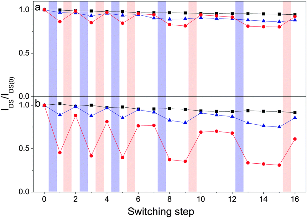 | ||
| Fig. 4 Normalized drain–source current as a function of repeatedly switching the DAEs between their open and closed states for (a) PCBM, and (b) ICBA devices (black squares = pristine material, red circles = DAE-FN blend, and blue triangles = DAE-F blend). Lines are drawn as guide for the eye. Irradiation is indicated by violet (λ = 320 nm, 30 s) and red (λ = 540 nm, 10 min) shaded areas. For details regarding the switching procedure see the ESI.† | ||
The original current is recovered after closed → open photoisomerization, proving that the current modulation indeed is an effect of the state of the DAEs. Noteworthy, both in the high and low current configurations, several readouts can be performed, demonstrating that the devices effectively can be regarded as memories. The fatigue resistance for the PCBM samples is quite good. A decrease in current of 8% for the PCBM/DAE-FN blend as compared to 6% for pristine PCBM devices is observed after 5 complete switching cycles and 17 transfer sweeps. For ICBA transistors, the fatigue is higher, with a current decrease of 39% for the ICBA/DAE-FN blend and 9% for pristine ICBA. The lower fatigue resistance for ICBA based devices compared to PCBM ones has been observed in bulk heterojunction solar cells.45 ICBA devices are also generally more prone to bias stress (see Fig. S10, ESI†). Blended devices show a comparable lower fatigue resistance than pristine ones. It is believed that the relatively lower fatigue resistance for the blended devices is to a high degree due to degradation of semiconductor and not DAE since the switching cycle efficiency is preserved for each individual cycle (see Table S5, ESI†), and solution spectroscopy shows hardly any sign of degradation during 11 full switching cycles for both DAE derivatives (see Fig. 2a and b). However, it cannot be ruled out that the lower fatigue resistance is a joint effect of both semiconductor and DAE degradation.
Electrical characterization of transistors
The charge carrier mobility in an organic thin film strongly depends on its structure and morphology. By blending a photochromic molecule into an organic semiconductor, the packing of the latter can be affected, and this can be reflected in a major change of the field-effect mobility (μ). To examine the effect of blending on the performance of the transistor μ was determined in the saturation regime for the pristine semiconductors as well as for the different blends (Table 1; for threshold voltages, output characteristics, and on/off ratios see Fig. S7, S9 and Table S4, (ESI†), respectively). The charge mobility of PCBM devices remains, within experimental error, unaffected by blending with the DAEs, and it amounts to ca. 0.01 cm2 V−1 s−1, in line with previous reports on similar PCBM transistors.42 For pristine ICBA μ is close to the literature values of 3.5 × 10⁻³ and 6 × 10⁻³ cm2 V−1 s−1.43,46 However, ICBA transistors are more affected by blending as the μ-value of the blends is 6 times lower than in the pristine devices. Low effects on mobility in semiconductor/DAE blends has been observed in the past, and then been rationalized with phase segregation.37| Channel length | Field-effect mobility 10−3![[thin space (1/6-em)]](https://www.rsc.org/images/entities/char_2009.gif) a (cm2 V−1 s−1) a (cm2 V−1 s−1) |
|||
|---|---|---|---|---|
| 2.5 μm | 5 μm | 10 μm | 20 μm | |
| a Standard deviation in parenthesis; see ESI for threshold voltages (Fig. S7), output characteristics (Fig. S8, ESI), and Ion/Ioff ratios (Table S4, ESI). | ||||
| PCBM | 44.1 (22.2) | 20.7 (1.1) | 11.5 (0.1) | 10.0 (2.9) |
| PCBM/DAE-FN | 33.5 (17.0) | 19.3 (9.5) | 6.9 (1.2) | 7.5 (1.0) |
| PCBM/DAE-F | 38.0 (16.5) | 22.3 (10.8) | 7.4 (4.5) | 6.1 (4.6) |
| ICBA | 8.95 (1.03) | 4.53 (0.49) | 3.05 (0.48) | 2.47 (0.38) |
| ICBA/DAE-FN | 1.41 (0.63) | 0.59 (0.27) | 0.37 (0.20) | 0.41 (0.20) |
| ICBA/DAE-F | 0.63 (0.29) | 1.15 (0.6) | 0.89 (0.42) | 0.39 (0.22) |
Morphology of blended films
To gain a further insight into the relatively low effect of the blending on the field-effect mobilities, 2D-GIXD, AFM and Auger spectroscopy were performed on pristine as well as blended films. The 2D-GIXD measurements showed that all films used in this study were to a high degree amorphous in structure (Fig. S12, ESI†). This is as expected, since PCBM is known to crystallize only under very specific processing conditions like thermal annealing,47 which has not been performed in this study. AFM imaging of the pristine fullerene films (Fig. 5 and Fig. S11, ESI†) showed smooth films with a few crystals on the top. Upon blending the films become much rougher and roundish structures 0.4–2.5 μm in size appear. Auger spectroscopy, which probes the chemical composition in the top 5 nm of the films, further reveals sulfur contents in the PCBM blends but not in the ICBA blends (see Fig. S13 and S14, ESI†). A higher sulfur ratio in the top part of the films, and thus, corresponding lower ratio inside the films, could explain the relatively lower mobilities of the ICBA blends compared to the PCBM blends. It also indicates that the roundish structures as seen by AFM for both ICBA and PCBM blended films cannot easily be rationalized to only contain one species of the binary blend for all cases. On the one hand, a complete inter-mixing of the two molecules would most likely result in a more pronounced decrease in charge mobility, since intercalation of DAEs in between fullerenes would hinder efficient charge transport among adjacent fullerenes. On the other hand, complete phase segregation would probably not be advantageous from a switching perspective, since the two materials would not physically and energetically interact leading to a smaller current modulation upon photoisomerization.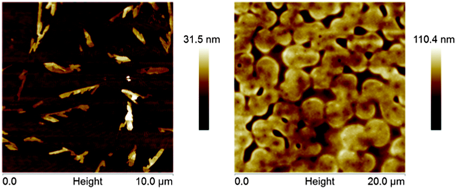 | ||
| Fig. 5 AFM images of pristine PCBM film (left) and PCBM/DAE-FN blended film, showing a comparably more rough film for the blended case than for the pristine semiconductor. | ||
Conclusion
In summary, we have demonstrated that the electron transport in an organic TFT can be photomodulated by blending an n-type molecular semiconductor with a suitable photochromic system. By comparing the effect on four different combinations of fullerenes/diarylethenes blends we found that the modulation of the current on photoisomerization depends on the ability of the photochromic molecule to act as an electron-accepting level in the active channel, which is in accordance to established theory. This clearly demonstrates the generality and versatility of our approach to introduce photoswitchable systems, which allow for light-controlled modulation of their energy levels to interact with either holes or electrons, depending on the nature of the matrix, i.e. p-type or n-type. Importantly, we have been able to implement photoaddressability in our hybrid photochromic-semiconductor transistors without sacrificing their intrinsic performance as they exhibit field-effect mobilities comparable to those of pristine devices, thereby demonstrating the effectiveness of our blending approach.Experimental section
Details on synthesis, solution spectroscopy, Auger spectroscopy and cyclic voltammetry of DAE-FN and DAE-F are provided in the ESI.†TFT preparation
Bottom-gate bottom-contact transistors were fabricated on heavily doped n-type silicon wafers serving as a gate electrode with 230 nm thick thermally grown, HMDS treated, SiO2 as the dielectric layer (Ci = 15 nF cm−2) and having pre-patterned gold electrodes (IPMS Fraunhofer). The pre-patterned substrates were cleaned by ultrasonication first in acetone and then in propanol, where after they were immersed in a 0.5 mM 1-undecanethiol solution (ethanol) over night. Pristine semiconductors or semiconductor/DAE blends (blend ratio 5/1 by weight in all cases) were spin-coated from chlorobenzene solution (10 and 20 mg ml−1, spin-coated at 500 and 800 rpm, for PCBM and ICBA devices, respectively) on the thiol treated samples in a nitrogen filled glovebox.Electrical characterization
Electrical characterization of the devices was performed at room temperature in a N2 atmosphere inside a glovebox, using a Cascade Microtech M150 probe station and a Keithley 2636A controlled by Labtracer software. Field-effect mobility and threshold voltage were extracted from the saturation regime. For switching experiments, a Polychrome V (Till Photonics) light source was used to irradiate the transistors at 320 ± 7.5 nm (180 μW cm−2) or 540 ± 7.5 nm (8.2 mW cm−2) for 30 s or 10 min, respectively. After irradiation the drain current was extracted at VG = 120 and 80 V for PCBM and ICBA transistors, respectively, taken from full ID–VG curves performed at VD = 40 V.Spectroscopy of thin films
Thin films of semiconductor/DAE blends were made by spin-coating (2500 rpm) the material dissolved in chloroform (5 to 1 ratio by weight) on glass substrates. The films were irradiated using light emitting diodes with emission wavelengths centered at 315 nm (150 μW cm−2; UVTOP310-HL-TO39, Roithner Lasertechnik) or 530 nm (3.8 mW cm−2; M530F1, Thorlabs). A JASCO V-630 spectrophotometer was used to record the absorbance spectra of the films, and the absorbance at 540 or 590 nm were used to monitor the absorbance evolution with time for the DAE-FN and DAE-F blends, respectively. The films on glass substrates were somewhat thicker than those prepared on the TFTs, which resulted in longer UV irradiation times needed for complete photoisomerization to occur due to optical inner filter effects.AFM characterization
A Veeco Dimension 3100 AFM running with a Nanoscope IV controller was used. AFM images were recorded in the intermittent contact (tapping) mode under ambient conditions using standard silicon cantilevers (Veeco MPP-11120-10).2D-GIXD
Diffraction patterns are collected using synchrotron radiation at the Stanford Synchrotron Radiation Lightsource (SSRL). Experiments were carried out with an incident beam of 12.7 keV at a grazing angle of 0.1° and expressed as a function of the scattering vector q = 4πsin(θ)/λ. Here θ represents half of the scattering angle, λ is the wavelength of the incident beam, qxy is the component of the scattering vector parallel to the substrate plane and qz is the component perpendicular to the substrate plane.Acknowledgements
Jutta Schwarz and Jana Hildebrandt are thanked for help with synthesis. This work was financially supported by EC through the IEF RESPONSIVE (PIEF-GA-2012-326665) and ITN iSwitch (GA no. 642196) as well as the ERC projects SUPRAFUNCTION (GA-257305) and LIGHT4FUNCTION (GA-308117), the International Center for Frontier Research in Chemistry (icFRC), the Agence Nationale de la Recherche through the LabEx CSC (ANR-10-LABX-0026_CSC), and the German Research Foundation (via SFB 658). A.S. gratefully acknowledges financial support from the NSF DMR award #1205752. D.T.D. thanks the support of the Stanford Graduate Fellowship and the NSF Graduate Research Fellowship.Notes and references
- U. Pischel, J. Andreasson, D. Gust and V. F. Pais, ChemPhysChem, 2013, 14, 28–46 CrossRef CAS PubMed.
- E. Orgiu and P. Samorì, Adv. Mater., 2014, 26, 1827–1845 CrossRef CAS PubMed.
- F. M. Raymo, Adv. Mater., 2002, 14, 401–414 CrossRef CAS.
- M. M. Russew and S. Hecht, Adv. Mater., 2010, 22, 3348–3360 CrossRef CAS PubMed.
- A. C. Fahrenbach, S. C. Warren, J. T. Incorvati, A. J. Avestro, J. C. Barnes, J. F. Stoddart and B. A. Grzybowski, Adv. Mater., 2013, 25, 331–348 CrossRef CAS PubMed.
- Y. Wakayama, R. Hayakawa and H.-S. Seo, Sci. Technol. Adv. Mater., 2014, 15, 024202 CrossRef.
- P. A. de Silva, N. H. Q. Gunaratne and C. P. McCoy, Nature, 1993, 364, 42–44 CrossRef.
- J. Kärnbratt, M. Hammarson, S. M. Li, H. L. Anderson, B. Albinsson and J. Andreasson, Angew. Chem., Int. Ed., 2010, 49, 1854–1857 CrossRef PubMed.
- A. P. de Silva and N. D. McClenaghan, Chem. – Eur. J., 2004, 10, 574–586 CrossRef PubMed.
- A. Credi, V. Balzani, S. J. Langford and J. F. Stoddart, J. Am. Chem. Soc., 1997, 119, 2679–2681 CrossRef CAS.
- H. Lin, Z. Wei, J. Xiang, W. Xu and D. Zhu, ChemPhysChem, 2009, 10, 1996–1999 CrossRef CAS PubMed.
- N. Matsui and T. Tsujioka, Org. Electron., 2014, 15, 2264–2269 CrossRef CAS.
- C. C. Jia, H. Li, J. L. Jiang, J. D. Wang, H. L. Chen, D. Cao, J. F. Stoddart and X. F. Guo, Adv. Mater., 2013, 25, 6752–6759 CrossRef CAS PubMed.
- S. J. van der Molen, J. H. Liao, T. Kudernac, J. S. Agustsson, L. Bernard, M. Calame, B. J. van Wees, B. L. Feringa and C. Schonenberger, Nano Lett., 2009, 9, 76–80 CrossRef CAS PubMed.
- A. C. Whalley, M. L. Steigerwald, X. Guo and C. Nuckolls, J. Am. Chem. Soc., 2007, 129, 12590–12591 CrossRef CAS PubMed.
- T. Kawai, Y. Nakashima and M. Irie, Adv. Mater., 2005, 17, 309–314 CrossRef CAS.
- A. Yassar, F. Garnier, H. Jaafari, N. Rebiere-Galy, M. Frigoli, C. Moustrou, A. Samat and R. Guglielmetti, Appl. Phys. Lett., 2002, 80, 4297–4299 CrossRef CAS.
- H. Choi, H. Lee, Y. Kang, E. Kim, S. O. Kang and J. Ko, J. Org. Chem., 2005, 70, 8291–8297 CrossRef CAS PubMed.
- M. J. Marsella, Z. Q. Wang and R. H. Mitchell, Org. Lett., 2000, 2, 2979–2982 CrossRef CAS PubMed.
- R. C. Shallcross, P. O. Korner, E. Maibach, A. Kohnen and K. Meerholz, Adv. Mater., 2013, 25, 4807–4813 CrossRef CAS PubMed.
- C. Sciascia, R. Castagna, M. Dekermenjian, R. Martel, A. R. S. Kandada, F. Di Fonzo, A. Bianco, C. Bertarelli, M. Meneghetti and G. Lanzani, J. Phys. Chem. C, 2012, 116, 19483–19489 CAS.
- P. Andersson, N. D. Robinson and M. Berggren, Adv. Mater., 2005, 17, 1798–1803 CrossRef CAS.
- X. F. Guo, D. Zhang, Y. Gui, M. X. Wax, J. C. Li, Y. Q. Liu and D. B. Zhu, Adv. Mater., 2004, 16, 636–640 CrossRef CAS.
- T. Tsujioka and K. Masuda, Appl. Phys. Lett., 2003, 83, 4978–4980 CrossRef CAS.
- D. Kim, H. Jeong, H. Lee, W.-T. Hwang, J. Wolf, E. Scheer, T. Huhn, H. Jeong and T. Lee, Adv. Mater., 2014, 26, 3968–3973 CrossRef CAS PubMed.
- A. J. Kronemeijer, H. B. Akkerman, T. Kudernac, B. J. van Wees, B. L. Feringa, P. W. M. Blom and B. de Boer, Adv. Mater., 2008, 20, 1467–1473 CrossRef CAS.
- V. Ferri, M. Elbing, G. Pace, M. D. Dickey, M. Zharnikov, P. Samorì, M. Mayor and M. A. Rampi, Angew. Chem., Int. Ed., 2008, 47, 3407–3409 CrossRef CAS PubMed.
- J. M. Mativetsky, G. Pace, M. Elbing, M. A. Rampi, M. Mayor and P. Samorì, J. Am. Chem. Soc., 2008, 130, 9192–9193 CrossRef CAS PubMed.
- M. Irie, Chem. Rev., 2000, 100, 1685–1716 CrossRef CAS PubMed.
- M. Irie and M. Mohri, J. Org. Chem., 1988, 53, 803–808 CrossRef CAS.
- M. Irie, T. Fukaminato, K. Matsuda and S. Kobatake, Chem. Rev., 2014, 114, 12174–12277 CrossRef CAS PubMed.
- P. Lutsyk, K. Janus, J. Sworakowski, G. Generali, R. Capelli and M. Muccini, J. Phys. Chem. C, 2011, 115, 3106–3114 CAS.
- N. Crivillers, E. Orgiu, F. Reinders, M. Mayor and P. Samorì, Adv. Mater., 2011, 23, 1447–1452 CrossRef CAS PubMed.
- H. T. Zhang, X. F. Guo, J. S. Hui, S. X. Hu, W. Xu and D. B. Zhu, Nano Lett., 2011, 11, 4939–4946 CrossRef CAS PubMed.
- Q. Shen, L. Wang, S. Liu, Y. Cao, L. Gan, X. Guo, M. L. Steigerwald, Z. Shuai, Z. Liu and C. Nuckolls, Adv. Mater., 2010, 22, 3282–3287 CrossRef CAS PubMed.
- R. Hayakawa, K. Higashiguchi, K. Matsuda, T. Chikyow and Y. Wakayama, ACS Appl. Mater. Interfaces, 2013, 5, 3625–3630 CAS.
- E. Orgiu, N. Crivillers, M. Herder, L. Grubert, M. Patzel, J. Frisch, E. Pavlica, D. T. Duong, G. Bratina, A. Salleo, N. Koch, S. Hecht and P. Samorì, Nat. Chem., 2012, 4, 675–679 CrossRef CAS PubMed.
- Y. Ishiguro, R. Hayakawa, T. Yasuda, T. Chikyow and Y. Wakayama, ACS Appl. Mater. Interfaces, 2013, 5, 9726–9731 CAS.
- F. L. E. Jakobsson, P. Marsal, S. Braun, M. Fahlman, M. Berggren, J. Cornil and X. Crispin, J. Phys. Chem. C, 2009, 113, 18396–18405 CAS.
- J. C. Hummelen, B. W. Knight, F. Lepeq, F. Wudl, J. Yao and C. L. Wilkins, J. Org. Chem., 1995, 60, 532–538 CrossRef CAS.
- Y. J. He, H. Y. Chen, J. H. Hou and Y. F. Li, J. Am. Chem. Soc., 2010, 132, 1377–1382 CrossRef CAS PubMed.
- T. D. Anthopoulos, C. Tanase, S. Setayesh, E. J. Meijer, J. C. Hummelen, P. W. M. Blom and D. M. de Leeuw, Adv. Mater., 2004, 16, 2174–2179 CrossRef CAS.
- H. Yu, H. H. Cho, C. H. Cho, K. H. Kim, D. Y. Kim, B. J. Kim and J. H. Oh, ACS Appl. Mater. Interfaces, 2013, 5, 4865–4871 CAS.
- C. M. Cardona, W. Li, A. E. Kaifer, D. Stockdale and G. C. Bazan, Adv. Mater., 2011, 23, 2367–2371 CrossRef CAS PubMed.
- T. Endale, E. Sovernigo, A. Radivo, S. Dal Zilio, A. Pozzato, T. Yohannes, L. Vaccari and M. Tormen, Sol. Energy Mater. Sol. Cells, 2014, 123, 150–158 CrossRef CAS.
- C. Z. Li, C. C. Chueh, H. L. Yip, J. Y. Zou, W. C. Chen and A. K. Y. Jen, J. Mater. Chem., 2012, 22, 14976–14981 RSC.
- E. Verploegen, R. Mondal, C. J. Bettinger, S. Sok, M. F. Toney and Z. A. Bao, Adv. Funct. Mater., 2010, 20, 3519–3529 CrossRef CAS.
Footnote |
| † Electronic supplementary information (ESI) available. See DOI: 10.1039/c5tc00401b |
| This journal is © The Royal Society of Chemistry 2015 |