
 Open Access Article
 This Open Access Article is licensed under a Creative Commons Attribution-Non Commercial 3.0 Unported Licence
The electronic and transport properties of (VBz)n@CNT and (VBz)n@BNNT nanocables
Xiu Yan
Liang
a,
Guiling
Zhang
*a,
Peng
Sun
a,
Yan
Shang
a,
Zhao-Di
Yang
a and
Xiao Cheng
Zeng
*b
aInnovative Research Team of Green Chemical Technology in University of Heilongjiang Province (2014TD007), College of Chemical and Environmental Engineering, Harbin University of Science and Technology, Harbin 150080, China. E-mail: guiling-002@163.com
bDepartment of Chemistry, University of Nebraska-Lincoln, Lincoln, NE 68588, USA. E-mail: xzeng1@unl.edu
First published on 3rd March 2015
Abstract
The electronic structures and transport properties of prototype carbon nanotube (CNT) (10,10) and boron–nitride nanotube (BNNT) (10,10) nanocables, including (VBz)n@CNT and (VBz)n@BNNT (where Bz = C6H6), are investigated using the density functional theory (DFT) and the non-equilibrium Green's function (NEGF) methods. It is found that (VBz)n@CNT shows a metallic character while (VBz)n@BNNT exhibits a half-metallic feature. Both (VBz)n@CNT and (VBz)n@BNNT nanocables show spin-polarized transport properties, namely, spin-down state gives rise to a higher conductivity than the spin-up state. For (VBz)n@CNT, the CNT sheath contributes the metallic transport channel in both spin-up and spin-down states, while the (VBz)n core is an effective transport path only in the spin-down state. For (VBz)n@BNNT, the BNNT sheath is an insulator in both spin-up and spin-down states. Hence, the transport properties of the (VBz)n@BNNT nanocable are attributed to the spin-down state of the (VBz)n core. The computed spin filter efficiency of (VBz)n@CNT is less than 50% within the bias of −1.0 to 1.0 V. In contrast, the spin filter efficiency of (VBz)n@BNNT can be greater than 90%, suggesting that the (VBz)n@BNNT nanocable is a very good candidate for a spin filter. Moreover, encapsulating (VBz)n nanowires into either CNTs or BNNTs can introduce magnetism and the computed Curie or Neél temperatures of both (VBz)n@CNT and (VBz)n@BNNT are higher than 2000 K. These novel electronic and transport properties of (VBz)n@CNT and (VBz)n@BNNT nanocables render them as potential nanoparts for nanoelectronic applications.
1 Introduction
Coaxial nanocables, a novel form of one-dimensional (1D) nanocomposite of a nanowire (NW) (core) enclosed inside a single or multi-wall nanotube (NT) (sheath), have been under much investigation in recent years.1–5 Various 1D materials with coaxial nanocable-like NW@NT structures have been synthesized in the laboratory, such as B@SiO2,6 SiC@SiO2,7 TiO2@SiO2,8 ZnSe@SiO2,9 Zn@ZnS,10 and ZnO@ZnS11. The functionality of nanocables can be broadened compared to that of single-component NWs due to the interplay between NWs and NTs. The combination of the two nanostructures may exhibit new electronic, magnetic, and conducting properties which could offer more prospects and opportunities for applications in nanodevices, magnetic data storage or molecular delivery platforms.12–19Carbon nanotubes (CNTs) and boron nitride nanotubes (BNNTs) are two known 1D hollow nanostructures for accommodating NWs and making nanocables. Various NWs of metals (Ni, Co, Fe, Cu, Se, Te, Ag),20–26 polymers (polyaniline, polythiophene),19,27,28 potassium halide,29 oxide (Fe3O4, Ga2O3),30–32 ZnS,33 or Si34 have already been introduced inside CNTs or BNNTs by using various experimental techniques. Typically, CNTs exhibit delocalized valence bonding character while BNNTs show localized ionic bonding character. So CNTs can be either metallic or semiconducting depending on their diameter and chirality, while BNNTs are insulating regardless of their morphology.35–40 This difference in electronic properties between CNTs and BNNTs inevitably leads to the different properties of corresponding nanocables. For example, there exists strong coupling between the encapsulated metal (Fe, Co, Ni, or Cu) NW and the CNT, which tends to have substantial modification of the electronic states. In contrast, the interaction between metal NWs and BNNTs is relatively weak and the original electronic structure of NWs is hardly changed by BNNTs.41–47
Recently, multidecker organometallic sandwich NWs have attracted growing attention owing to their potential applications in molecular electronic and magnetic devices.48–57 A number of such multidecker organometallic sandwich NWs have been synthesized.58,59 In particular, a NW system under intensive investigation is the vanadium–benzene multidecker (VBz)n (Bz = C6H6) NW.60 The synthesis of (VBz)n NWs can be realized from reaction of laser-vaporized metal atoms with C6H6 in a He atmosphere.48–49,61 Previous experimental studies have shown that in (VBz)n NWs the unpaired electrons on the V atoms are coupled ferromagnetically (FM).62 Later theoretical studies of (VBz)n NWs confirm this FM feature, and also suggest that the ground state of the (VBz)n NWs exhibits half metallicity (i.e., one spin channel is metallic while the other spin channel is insulating) and spin filter effect.63,64 The FM sandwich (VBz)n NWs are therefore promising candidates as nanomagnetic building blocks in applications such as recording media or spintronic devices.65 Other novel sandwich complexes including (η5-Cp)FeC60R5 (R = Me, Ph; Cp = C5H5)66 and ferrocene67 have also been successfully introduced into CNTs to make a class of self-assembled hybrid structures. We recently showed from ab initio calculations that encapsulating (C60V)n NWs or ferrocene based molecules into CNTs or BNNTs can result in new physical properties.68,69 Here, we show that (VBz)n NWs can also be introduced into CNTs or BNNTs to form nanocables with multifunctional properties. Particular attention in this study is focused on the electronic and transport properties of (VBz)n@CNT and (VBz)n@BNNT nanocables as well as the differences in these properties between the nanocables and their CNT, BNNT, and (VBz)n components.
2 Models and computational methods
Metallic CNTs (10,10) and insulating BNNTs (10,10) are selected as prototype host NTs. For computing electronic structures, the infinite (VBz)n@CNT and (VBz)n@BNNT systems are modeled using the periodic condition in the axial direction. For computing transport properties, the two-probe devices are adopted. As a benchmark test, we have computed electronic properties based on infinite NT and (VBz)n systems and transport properties based on the two-probe devices for pure CNT (10,10), BNNT (10,10), and bare (VBz)n systems.For periodic systems, the supercell contains six layers of the NT (120 atoms) and two units of VBz [i.e., (VBz)2] inside the NT (Fig. 1) because the lattice parameter of the (VBz)2 NW (∼7.38 Å) nearly matches the lattice parameter of the supercell of CNTs (10,10) and BNNTs (10,10) (∼7.30 Å). In addition, such a supercell containing two V atoms can be used to study magnetic coupling between V atoms. The nanocables are separated by 20.0 Å vacuum to neglect tube–tube interaction. All the periodic systems are fully optimized until the maximum absolute force is less than 0.02 eV Å−1.
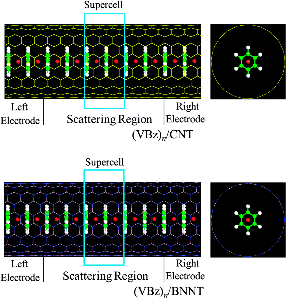 | ||
| Fig. 1 Optimized structures of (VBz)n@CNT and (VBz)n@BNNT nanocables, and the two-probe devices for electron transport computation. For the periodic systems, we denote CNT as 1a, (VBz)n@CNT as 1b, BNNT as 2a, (VBz)n@BNNT as 2b, and (VBz)n as c, and for the two-probe devices, we denote CNT as D-1a, (VBz)n@CNT as D-1b, BNNT as D-2a, (VBz)n@BNNT as D-2b, and (VBz)n as D-c. Color code for the core atoms: V (red); H (white); C (green). | ||
For the two-probe devices, we take six optimized unit cells, i.e., (VBz)6@CNT or (VBz)6@BNNT, as the central scattering region, which is long enough (>21.0 Å) to separate the left and right electrodes. To compute intrinsic transport properties of the nanocables, we select 1/3 in length of the scattering region as each of the two opposing electrodes (Fig. 1). Transport current is computed by changing the applied bias in steps of 0.2 V in the range of −1.0 to 1.0 V.
All the computations for both infinitely long and two-probe systems are performed using combined DFT/NEGF methods, implemented in the software package Atomistix ToolKit (ATK).70–73 A generalized gradient approximation (GGA) within the Perdew–Burke–Ernzerhof (PBE) formalism is employed to describe the exchange correlations between electrons. The spin polarization of the V atom is considered in all calculations. The on-site correlation effects among the 3d electrons of the V atom are accounted for by using the GGA + U scheme,73 where the parameter U–J is set to be 3.4. A double-ζ basis with polarization (DZP) is used for all atoms. A (1 × 1 × 100) k-point string in the Brillouin zone (x, y, z directions, respectively) is adopted, and 150 Ry cutoff energy is applied to describe the periodic wave function. For the sake of simplification, hereafter, we denote CNT as 1a, (VBz)n@CNT as 1b, BNNT as 2a, (VBz)n@BNNT as 2b, and (VBz)n as c for the periodic systems. We also denote CNT as D-1a, (VBz)n@CNT as D-1b, BNNT as D-2a, (VBz)n@BNNT as D-2b, and (VBz)n as D-c for the two-probe systems.
3 Results and discussion
Fig. 1 shows the optimized structures of nanocables (VBz)n@CNT and (VBz)n@BNNT. First, we show the results of geometry, magnetism, and band structures of the infinitely long nanocables of 1b and 2b, followed by transport properties computed based on the two-probe devices of D-1b and D-2b.3.1 Stability and geometry
Computed total energies per supercell for the optimized 1b and 2b are listed in Table 1. The antiferromagnetic (AFM) state and the ferromagnetic (FM) state of the two V atoms are both considered. It is known that pure (VBz)n nanowire favors FM ground state.62,63 Notably, regardless of a CNT or BNNT sheath, the neighboring V atoms of the encapsulated (VBz)n still favor the FM coupling as reflected from the lower energy of the FM state compared to the AFM state in both 1b and 2b. Hereafter, we mainly focus on the FM state of 1b and 2b and discuss associated electronic and transport properties.| Species | E Tot,FM/eV | E Tot,AFM/eV | ΔEFM–AFM/meV | ΔEr,FM/eV | J/meV | T C(N)/K |
|---|---|---|---|---|---|---|
| a Computed total energies in the FM or AFM state per supercell (ETot,FM, ETot,AFM), the energy difference per supercell between FM and AFM states (ΔEFM–AFM), the reaction energy per supercell in the FM state (ΔEr,FM), the exchange parameter per supercell (J), the Curie or Neél temperatures (TC(N)), the Mulliken populations of V valence orbitals (PV(3d)↑, PV(3d)↓, PV(4s)↑, PV(4s)↓; the ↑ and ↓ denote spin-up and spin-down, respectively), the charge distributions on V, Bz, and NT (qV, qBz, qNT), the local magnetic moments corresponding to the V 3d and 4s states (SV(3d) and SV(4s)), the magnetic moment of the V atom (Sv), and total magnetic moment per supercell (STot). | ||||||
| 1b | −24742.12649 | −24741.51593 | −610.56 | −1.060 | −610.56 | 2365.92 |
| 2b | −27095.90460 | −27095.09389 | −810.71 | −0.016 | −810.71 | 3133.78 |
| Species | Mulliken population, P | Charge, q/a.u. | Magnetic moment, S/μB | ||||||||||
|---|---|---|---|---|---|---|---|---|---|---|---|---|---|
| P V(3d)↑ | P V(3d)↓ | P V(4s)↑ | P V(4s)↓ | q V | q Bz | q NT | S V(3d) | S V(4s) | S v | S NT | S Bz | S Tot | |
| 1b | 2.64 | 0.48 | 0.05 | 1.0 | 0.83 | −0.43 | −0.4 | 2.16 | −0.95 | 1.31 | 0.0 | −0.01 | 1.20 |
| 2b | 2.71 | 0.54 | 0.05 | 1.0 | 0.70 | −0.72 | 0.02 | 2.17 | −0.95 | 1.22 | 0.0 | −0.23 | 0.99 |
The chemical stability of the encapsulated (VBz)n is evaluated by computing the reaction energy per supercell for the net reaction [NT + (VBz)2 → (VBz)2@NT − ΔEr] where NT represents the nanotube in a supercell. Here, the computed reaction energies ΔEr are −1.060 and −0.016 eV for 1b and 2b, respectively (cf.Table 1). The negative values indicate exothermic reactions. Hence, incorporation of (VBz)n into either CNTs or BNNTs is energetically quite favorable.
The optimized supercell length (L) in the axial direction, the radii of NTs (R), the face-to-face distances between adjacent Bz (r1), the average C–C bond lengths in Bz (r2), and the distances between the H atom of Bz and the nearest atom on NTs (r3) for 1b and 2b are given in Table 2. The incorporation of the (VBz)n into NTs causes no changes in the supercell length as reflected from the identical values of L compared to the bare NT. The NT radii R of 1b and 2b are slightly expanded compared with bare 1a and 2a, respectively. The distances r1 are 3.692 Å for both 1b and 2b, slightly longer than that (3.40 Å) in pure (VBz)n.74–76 The computed C–C bond lengths in the Bz r2 range from 1.458 Å to 1.461 Å, very close to the experimentally measured bond length for (VBz)n (1.44 Å).77 The shortest distances between the H atom of Bz and the nearest atom of NTs (r3) are in the range of 4.284−4.456 Å.
| Species | L/Å | R/Å | r 1/Å | r 2/Å | r 3/Å |
|---|---|---|---|---|---|
| a The supercell length along the axial direction (L), the radii of nanotube (R), the face-to-face distances between adjacent Bz (r1), the average C–C bond lengths in Bz (r2), and the distances between H atom of Bz and the nearest atom on nanotube (r3). | |||||
| Pure CNT 1a | 7.383 | 13.568 | |||
| (VBz)n@CNT 1b | 7.383 | 13.799 | 3.692 | 1.458 | 4.284 |
| Pure BNNT 2a | 7.384 | 13.669 | |||
| (VBz)n@BNNT 2b | 7.384 | 14.172 | 3.692 | 1.461 | 4.456 |
3.2 Band structures
Fig. 2 displays the computed band structure of c, and the corresponding Kohn–Sham orbitals near the Fermi level (Ef). It is known that the five 3d orbitals of V atom split into a 3dz2 (a1) orbital and two sets of doubly degenerate 3dxy,x2−y2 (e2) and 3dxz,yz (e1) orbitals under the Bz ligand field with D6h symmetry. Here, the (VBz)2 supercell contains two V atoms which contribute ten 3d orbitals to couple with the Bz π orbitals, thereby resulting in ten bands: and
and  bands, two sets of doubly degenerate
  and
and  bands, and two sets of doubly degenerate
  and
and  bands (cf.Fig. 2). The
  and
and  bands are far below the Ef. In the spin-up state (cf.Fig. 2(a)), the
  and
and  bands correspond to the valence and conduction band, respectively, which give a band gap of ∼1.80 eV, suggesting a semiconducting character. In the spin-down state, the valence
  band and the conduction
  band cross at the Ef (cf.Fig. 2(b)), showing a metallic character. Thus, the (VBz)n NW is indeed a half metal. This result is consistent with experimental observation62 and other theoretical investigations.63–65
 | ||
| Fig. 2 Computed band structures (left panels) of pure (VBz)n and the Kohn–Sham orbitals (middle and right panels) corresponding to the energy levels (highlighted in color lines) near Ef at the Γ point. The iso-surface value is 0.05 (e Å−3). | ||
Fig. 3 displays the computed band structures of 1a (CNTs) and the nanocable 1b ((VBz)n@CNT) as well as the corresponding Kohn–Sham orbitals near the Fermi level Ef. For 1a, the valence bands I and II and the conduction bands III and IV cross at the Ef with a large dispersion, reflecting typical metallic characteristics (cf.Fig. 3(a)). For 1b, the spin-up state clearly shows different features from the spin-down state. The unoccupied V  and
and  orbitals are far away from the Fermi level Ef and thus not plotted in Fig. 3(b) and (c). Compared to 1a, one can see that the CNT bands III and IV downshift slightly in the spin-up state of 1b (cf.Fig. 3(b)), and both bestride the Ef. As such, the CNT π state in the spin-up state behaves like partial-filled and should dominate the electron transport. The occupied (VBz)n
 states are located just below the Ef, serving as valence bands, and cross with the CNT bands III and IV (cf.Fig. 3(b)). The (VBz)n
 states are mainly originated from V 3dxz,yz states as shown from the plotted Kohn–Sham orbitals. Hence, the V atom can also contribute to the electron transport via electron hopping to the CNT sheath. For the spin-down state, the CNT bands III and IV downshift significantly to bestride the Ef (cf.Fig. 3(c)). Thus, the CNT π state in the spin-down state still serves as a major transport pathway. It is noteworthy that the (VBz)n
 bands upshift significantly to cross the Ef, serving as a half-filled band. This indicates that the core (VBz)n NW also offers a notable transport pathway along the axial direction. These results can be reflected from the projected density of states (PDOS) as well in Fig. 4. Evidently, the CNT π states of 1a and 1b exhibit similar PDOS features, e.g., peaks and broad valleys around the Ef. Thus, the CNT π states are still the main transport channels even with the core (VBz)n NW. For the spin-up state, a similar V-CNT hopping channel arises as the V 3d PDOS peak appears right below the Ef. For the spin-down state, both the Bz π PDOS and V 3d PDOS cross the Ef with a half-filled character, again a manifestation of the transport channel along (VBz)n NWs. In summary, for nanocable 1b, both the CNT sheath and the (VBz)n core can provide metal-like transport pathways. Moreover, electron hopping from the core (VBz)n to the CNT sheath may contribute to electron transport.
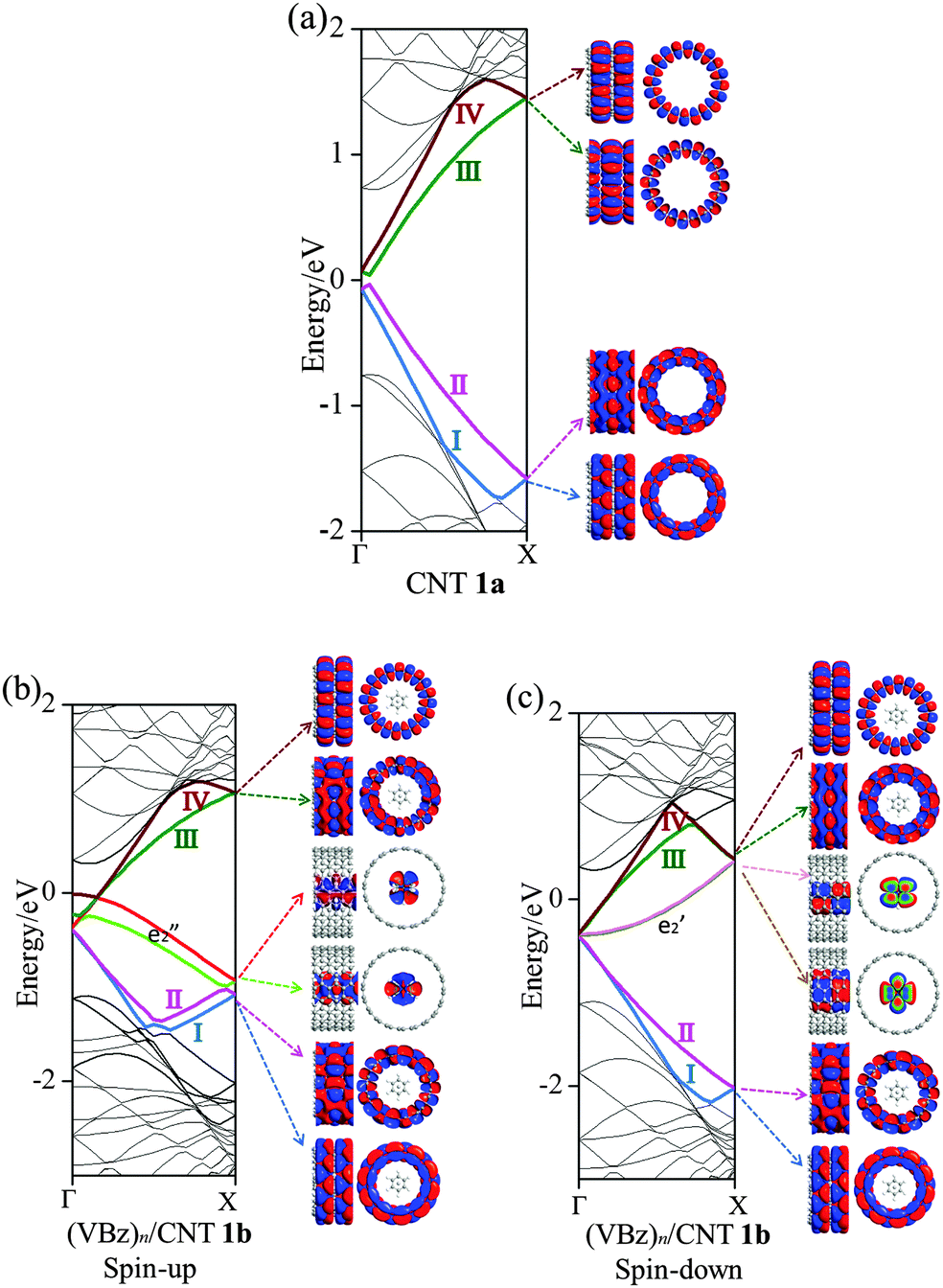 | ||
| Fig. 3 Computed band structures (left panels) of pure CNT and (VBz)n@CNT nanocable and the Kohn–Sham orbitals (middle and right panels) corresponding to the energy levels (highlighted in color lines) near Ef at the Γ point. The iso-surface value is 0.05 (e Å−3). | ||
 | ||
| Fig. 4 Computed projected density of states (PDOS) of (VBz)n@CNT and (VBz)n@BNNT nanocables. For comparison, PDOS of pure CNT and BNNT systems are also presented. | ||
In Fig. 5, computed band structures of 2a (BNNTs) and nanocable 2b ((VBz)n@BNNT) are plotted along with the associated Kohn–Sham orbitals near the Ef. For 2a, as expected, the valence band I is separated from the conduction band II by a large band gap of 4.64 eV (cf.Fig. 5(a)). By comparing Fig. 5(b) with 2(a), and Fig. 5(c) with 2(b), we find that the bands originated from the (VBz)n NW are little affected even when inside the BNNT. In the spin-up state of 2b, the (VBz)n ,
,  ,
,  , and
, and  bands are located between the BNNT band I and the Ef. The (VBz)n
 state serves as the valence band and the BNNT π state as the conduction band (cf.Fig. 5(b)). As a result, the band gap of 2b is 1.25 eV, reduced from 4.64 eV of 2a, showing a semiconducting feature. In the spin-down state, both the valence band
  and the conduction band
  fall in the band gap region of BNNTs and cross at the Ef just as in the case of c (cf.Fig. 5(c)). As such, the (VBz)n core can offer a metal-like transport path. Overall, encapsulating (VBz)n into BNNTs results in the half-metallic properties for 2b. These properties can be further confirmed from the PDOS in Fig. 4. The BNNT retains the insulating property in 2b as the BNNT π PDOS are largely separated from the Ef. In the case of the spin-up state, a band gap of about 1.25 eV can be seen between the valence V 3d PDOS and the conduction BNNT π PDOS, showing the semiconducting character. In the case of the spin-down state, the Bz π PDOS peak is located just across the Ef, indicating a metallic character. Thus, nanocable 2b displays a half-metallic character just like pure c, different from the metallic character of the nanocable 1b.
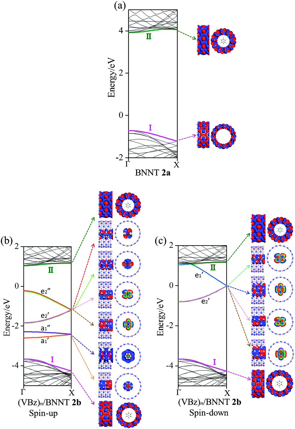 | ||
| Fig. 5 Computed band structures (left panels) of the pure BNNT and (VBz)n@BNNT nanocables and the Kohn–Sham orbitals (middle and right panels) corresponding to the energy levels (highlighted in color lines) near Ef at the Γ point. The iso-surface value is 0.05 (e Å−3). | ||
3.3 Magnetic properties
As shown in Table 1, both 1b and 2b nanocables favor the FM ground state. Table 1 also gives calculated Mulliken population and magnetic moment S for the FM state of 1b and 2b. On one hand, the spin-up V 4s and 3d orbitals donate electrons to the Bz π-orbitals to form coordinate bonds. On the other hand, the Bz π-orbitals feedback electrons to the spin-down V 3d orbital to form feedback bonds. For 1b, the spin-up V 4s orbital entails only 0.05 electron, i.e., 0.95 electron of the V 4s orbital is transferred to the Bz π-orbital, leading to a negative magnetic moment of SV(4s) = −0.95 μB. The electron number in the spin-up V 3d orbital decreases to 2.64 from 3.0, i.e., 0.36 electron is transferred to the Bz π-orbitals. Meanwhile, the Bz feedback 0.48 electron to the spin-down V 3d orbital. Therefore, the V 3d state generates a positive magnetic moment of SV(3d) = 2.16 μB. Overall, each V atom in (VBz)n@CNT possesses 4.17 valence electrons (PV(3d)↑ + PV(3d)↓ + PV(4s)↑ + PV(4s)↓ in Table 1). The other 0.83 electron from the V atom is distributed over the Bz and the sheath CNT. So the Bz and the CNT bear −0.43e and −0.40e charge, respectively.Notably, as shown in Table 1, CNTs or BNNTs in the nanocable do not show FM behavior as reflected from the zero value of SNT. The integer magnetic moment STot = 1.20 μB for each unit cell VBz@CNT mainly arises from the V atom, larger than that for pure c (S = 1.0 μB64). In 2b, the V 4s orbital gives rise to a SV(4s) = −0.95 μB magnetic moment, while the V 3d orbital induces 2.17 μB magnetic moment, leading to a value of SV = 1.22 μB for each V atom in 2b. The V atom possesses 4.3 valence electrons. Different from 1b, the donated 0.7 electron from each V in 2b distributes over the Bz only. The unit cell of BNNTs in 2b transfers 0.02 electrons to the Bz. These additional electrons given to Bz are partially coupled ferromagnetically, resulting in a magnetic moment of SBz = −0.23 μB. Thus, the integer magnetic moment is reduced to 0.99 μB for each unit cell of 2b, less than that in 1b and comparable to that in pure c. The exchange parameter J, which can be estimated by the energy difference between FM and AFM configurations, is about −610.56 meV and −810.71 meV per supercell (containing two V atoms) for 1b and 2b, respectively (cf.Table 1). The J value of 2b is higher than that of 1b. We also estimate the Curie or Neél temperatures, TC(N), of the nanocables using the formula 3/2kBTC(N) = J/2 (see Table 1). The estimated Curie or Neél temperatures for both 1b and 2b are higher than 2000 K, suggesting that the FM state of 1b and 2b can be highly stable even at elevated temperatures. The magnetic behavior of 1b and 2b nanocables is also reflected by uneven PDOS distribution in the spin-up and spin-down states as shown in Fig. 4. The spin polarization is mainly due to the V atoms.
3.4 Transport properties
To analyze the effect of core (VBz)n on the transport properties of the two nanocables, we construct a model system such that six unit cells, i.e., (VBz)6@CNT or (VBz)6@BNNT, are sandwiched between two electrodes, forming a two-probe device as described in Section 2 (cf.Fig. 1). Computation results suggest that electric conductivities of the two-probe devices are consistent with the electronic structures of the corresponding infinitely long nanocable systems.The computed I–V curves based on the two-probe devices are shown in Fig. 6(a). The magnitude of the total current of pure D-1a is on the order of 10−4 A, showing good metallic properties, whereas the magnitude of total current of pure D-c is two orders of magnitude lower than that of D-1a. The conductivity of D-1a satisfies Ohm's law, while D-c gives a nonlinear I–V curve in the bias range of −1.0 to 1.0 V. Notably, the conductivity is enhanced when (VBz)n is enclosed inside CNTs by comparing the total current of D-1a with D-1b. This behavior is consistent with the computed electronic structures. Fig. 6(a) shows that pure D-2a exhibits features of an insulator with nearly zero current. Clearly, the nanocable D-2b displays almost the same conductivity as pure D-c, indicating that the (VBz)n NW plays the main role in electron transport in D-2b, again consistent with computed electronic structures.
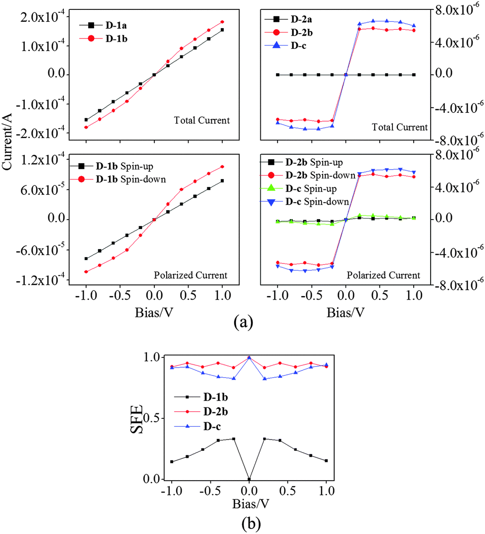 | ||
| Fig. 6 (a) Computed I–V curves of two-probe devices of D-2a and D-2b. For comparison, the I–V curves for pure CNT D-1a and BNNT D-1b two-probe devices are also presented. (b) Computed SFE curves under different V for D-1b, D-2b, and D-c systems. | ||
For FM D-1b, D-2b, and D-c systems, the spin-up current (I↑) and spin-down current (I↓) are computed. The conductivities are spin-state dependent within the bias range of −1.0 to 1.0 V. The spin-down state gives a higher conductivity than the spin-up state, suggesting that both nanocables and D-c can be a spin filter, again consistent with electronic structures of infinitely long 1b, 2b, and c systems. Another study also indicates that (VBz)n coupled to Ni or Co electrodes can be a nearly perfect spin filter.78
The spin filter efficiency (SFE) at zero bias voltage can be evaluated from the transmission by using the formula
 | (1) |
 | (2) |
The SFE curves under different bias for D-1b, D-2b, and D-c systems are shown in Fig. 6(b). The SFE values of D-1b are all below 50%, whereas D-2b gives high values for SFE (>90%). Evidently, the SFE values of D-2b are higher than those of D-c. So the D-2b system exhibits remarkable spin-polarized transport properties, which may be exploited as a new kind of spin filter.
Effects of (VBz)n NWs on the transport properties of D-1b and D-2b can be also analyzed from other aspects such as energy spectra (ES), molecular projected self-consistent Hamiltonian (MPSH) states, transmission spectra (TS), and electrostatic potentials (EP). The results together with those of D-1a and D-2a are depicted in Fig. 7–10.
 | ||
| Fig. 7 Computed energy spectra (left panels) of (a), (b) D-1a and (c)–(f) D-1b two-probe devices. The MPSH states (middle and right panels) correspond to the energy levels (highlighted in color lines) near Ef. The iso-surface value is 0.05 (e Å−3). | ||
 | ||
| Fig. 8 Transmission spectra (TS) of D-1a, D-1b, D-2a, and D-2b two-probe devices. | ||
 | ||
| Fig. 9 Computed energy spectra (left panels) of (a), (b) D-2a and (c)–(f) D-2b two-probe devices and the MPSH states (middle and right panels) corresponding to the energy levels (highlighted in color lines) near Ef. The iso-surface value is 0.05 (e Å−3). | ||
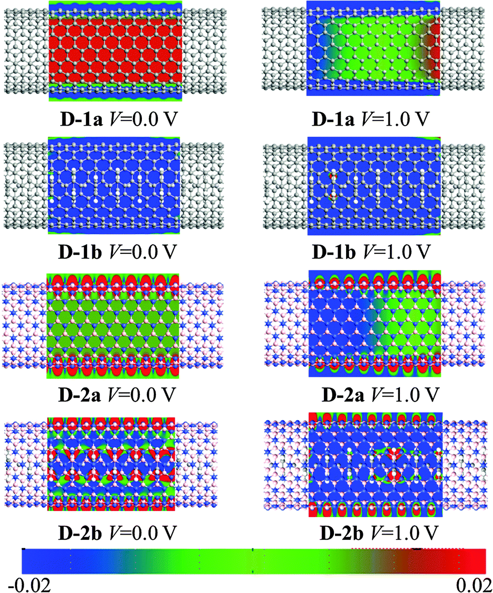 | ||
| Fig. 10 Computed contour plot of potential distribution for D-1a, D-1b, D-2a, and D-2b at 0.0 and 1.0 V. Blue (red) represents low (high) potential. | ||
Fig. 7 gives the ES and MPSH states for D-1a and D-1b. For the pure D-1a, ES shows little change at 1.0 V bias. The HOMO and LUMO (I and II in Fig. 7(a) and (b)) MPSH states of D-1a delocalize over the CNT at 0.0 and 1.0 V bias, indicating that the CNT is an effective transport path. For the spin-up state of D-1b, at 0.0 V bias, two (VBz)n states (i and ii in Fig. 7(c)) appear just below the Ef and exhibit a delocalized character, in line with the band structures of 1b. The CNT π states (I and II in Fig. 7(c)) of D-1b are nearly the same as those of D-1a. The external 1.0 V bias exerts little effect on the ES and MPSH states of CNT I and II states of D-1b (cf.Fig. 7(d)). However, the MPSH states of i and ii levels of (VBz)n shrink considerably and become localized on one side under 1.0 V bias. The (VBz)n states do not appear above the Ef within the bias region of −1.0–1.0 V. The LUMO is mainly dominated by the CNT II state. Therefore, in the spin-up state of D-1b, electron transport is still dominated by the CNT. The (VBz)n NW in D-1b cannot offer an effective transport channel; electron hopping from (VBz)n to CNTs may contribute to electron transport.
Fig. 8 shows the TS distribution for D-1a and D-1b. Like D-1a, a flat valley feature can be seen around Ef at both 0.0 and 1.0 V bias for the spin-up state of D-1b. This again demonstrates that the CNT dominates electron transport in the spin-up state of D-1b. For the spin-down state of D-1b, the ES, MPSH states, and TS show clearly different characteristics from the spin-up state. At 0.0 V bias, four (VBz)n states (i–iv in Fig. 7(e)) appear in the energy region of −1.0 to 1.0 eV: i and ii are located between Ef and the CNT I, while iii and iv are located above the CNT II. If 1.0 V bias is applied, (VBz)n iii and iv levels downshift and come close to the CNT II (cf.Fig. 7(f)). The delocalized feature of the MPSH states of CNT I and II demonstrates high efficiency in electron transport along CNT. The MPSH states of (VBz)n i and ii are dispersed over the left side while those of (VBz)n iii and iv are scattered over the right side. So electrons can permeate from the left to the right of (VBz)n. Thus, in the spin-down state of D-1b, the (VBz)n NW also behaves as an effective transport path besides the CNT. This is the reason why the spin-down state of D-1b exhibits higher conductivity than the spin-up state as shown in Fig. 6(a). The TS in Fig. 8 also shows that the spin-down state contributes more peaks around the Ef than the spin-up state.
Fig. 9 plots the ES and MPSH states at 0.0 and 1.0 V bias for D-2a and D-2b. The HOMO (I) and LUMO (II) of D-2a result in a large energy gap of 4.22 and 3.56 eV at 0.0 and 1.0 V, respectively (Fig. 9(a) and (b)). At 0.0 bias and in the spin-up state of D-2b, the (VBz)n i and ii states appear below the Ef and above the BNNT I state (cf.Fig. 9(c)). The (VBz)n i and ii states turn into the HOMO, and the BNNT II state is still the LUMO in D-2b. This is in line with the band structure of periodic 2b. At 1.0 V bias, the (VBz)n states iii and iv are moved toward Ef and changed into LUMO (cf.Fig. 9(d)), that is, both HOMO and LUMO of the spin-up state of D-2b stem from the (VBz)n NW under the external bias, giving an energy gap of 0.35 eV. In the case of the spin-down state of D-2b, both the HOMO and LUMO are contributed by the (VBz)n states regardless of the bias voltage (cf.Fig. 9(e) and (f)). Evidently, the HOMO–LUMO gap of spin-down state of D-2b is narrowed to 0.07 eV at 1.0 V from 0.11 eV at 0.0 V. This 0.07 eV value is much smaller than that of the spin-up state at 1.0 V (0.35 eV). In addition, the MPSH states of the (VBz)n i–iv levels in the spin-down state delocalize more strongly than in the spin-up state, leading to a more effective spin-down transport channel. Hence, the transport properties of D-2b are dominated by the spin-down state of the (VBz)n NW. Further confirmation can be made through the TS distributions in Fig. 8. The spin-up state shows no TS contribution both at 0.0 or 1.0 V bias, while the spin-down state shows a peak at the Ef under both 0.0 and 1.0 V. Thus, D-2b displays half-metallic properties arising from the (VBz)n NW and should have a high SFE of >90%. In contrast, D-1b shows a metallic character dominated by CNTs, and thus its SFE is <50%.
In addition, we calculate the potential distribution to investigate the barrier in the electron transport along the D-2a and D-2b by comparing with D-1a and D-1b. The results are plotted in Fig. 10. Clearly, the CNT serves as an effective transport channel in D-1a (blue color). With the (VBz)n core, both the CNT and (VBz)n act as effective transport paths in D-1b as reflected by the blue color of the whole nanocable. In contrast, the BNNT exhibits insulating behavior (red color). The (VBz)n core opens a transport pathway for the D-2b nanocable.
4 Conclusions
We have investigated the electronic and transport properties of a novel form of (VBz)n@CNT and (VBz)n@BNNT nanocables by means of DFT and NEGF methods. We find that endohedral encapsulation of (VBz)n into CNTs (10,10) or BNNTs (10,10) is energetically favorable. Upon encapsulation of (VBz)n both (VBz)n@CNT and (VBz)n@BNNT nanocables exhibit magnetism. More importantly, the ferromagnetic (VBz)n@CNT or (VBz)n@BNNT is predicted to possess a very high Curie or Neel temperature, all above 2000 K, suggesting a potential candidate as the magnetic nanopart. Conductivities of (VBz)n@CNT and (VBz)n@BNNT nanocables are dependent on the spin state: the spin-down state gives a higher conductivity than the spin-up state. (VBz)n@CNT shows a metallic character while (VBz)n@BNNT exhibits half-metallic feature. In the spin-up state of (VBz)n@CNT, the electron transport are dominated by the CNT sheath, while the (VBz)n core cannot offer an effective transport channel. In the spin-down state of (VBz)n@CNT, besides the CNT, the (VBz)n core also offers another effective transport pathway. For (VBz)n@BNNT, the BNNT is essentially an insulator sheath, while the transport properties of (VBz)n@BNNT nanocable are mainly contributed by the spin-down state of the (VBz)n core. Values of the spin-filter efficiency of (VBz)n@CNT are less than 50%, whereas those of (VBz)n@BNNT amount to more than 90%. This suggests that D-2b nanocable possesses excellent spin-polarized transport properties, which may be viewed as a new kind of spin filter. Encapsulating (VBz)n NWs into either CNTs or BNNTs can effectively tune the electronic and transport properties and both nanocables can be potentially used as functional nanodevices.Acknowledgements
GLZ is supported by grants from the NSFC (51073048, 51473042), the SF for leaders in the Academy of Harbin City of China (2013RFXXJ024), and the science foundation for backup leader of leading talent echelon in Heilongjiang province. XCZ is supported by a grant from the US National Science Foundation (NSF) through the Nebraska Materials Research Science and Engineering Center (MRSEC) (grant No. DMR-1420645).References
- A. M. Morales and C. M. Lieber, Science, 1998, 279, 208 CrossRef CAS.
- Y. Zhang, K. Suenaga, C. Colliex and S. Iijima, Science, 1998, 281, 973 CrossRef CAS.
- W. S. Shi, H. Y. Peng, L. Xu, N. Wang, Y. Tang and S. T. Lee, Adv. Mater., 2000, 12, 1927 CrossRef CAS.
- W. Z. Wang, L. Sun, Z. Fang, L. Y. Chen and Z. D. Zhang, Cryst. Growth Des., 2009, 9, 2117 CAS.
- S. J. Guo, J. Li, W. Ren, D. Wen, S. J. Dong and E. K. Wang, Chem. Mater., 2009, 21, 2247 CrossRef CAS.
- L. M. Cao, H. Tian, Z. Zhang, M. Feng, Z. J. Zhan, W. K. Wang and X. Y. Zhang, Cryst. Growth Des., 2008, 8, 4350 CAS.
- H. F. Zhang, C. M. Wang and L. S. Wang, Nano Lett., 2002, 9, 941 CrossRef.
- M. Wu, J. Phys. Chem. C, 2008, 112, 13192 Search PubMed.
- M. Wang, G. T. Fei, X. G. Zhu, B. Wu and L. D. Zhang, J. Phys. Chem. C, 2009, 113, 8730 CAS.
- J. Zhang, F. H. Jiang and Z. H. Dai, J. Phys. Chem. C, 2010, 114, 294 CAS.
- C. L. Yan and D. F. Xue, J. Phys. Chem. B, 2006, 110, 25850 CrossRef CAS PubMed.
- B. Burteaux, A. Claye, B. W. Smith, M. Monthioux, D. E. Luzzi and J. E. Fischer, Chem. Phys. Lett., 1999, 310, 21 CrossRef CAS.
- J. Sloan, R. E. Dunin-Borkowski, J. L. Hutchison, K. S. Coleman, V. C. Williams, J. B. Claridge, A. P. E. York, C. Xu, S. R. Bailey, G. Brown, S. Friedrichs and M. L. H. Green, Chem. Phys. Lett., 2000, 316, 191 CrossRef CAS.
- H. Kataura, Y. Maniwa, T. Kodama, K. Kikuchi, K. Hirahara, K. Suenaga, S. Iijima, S. Suzuki, Y. Achiba and W. Krätschmer, Synth. Met., 2001, 121, 1195 CrossRef CAS.
- K. Hirahara, S. Bandow, K. Suenaga, H. Kato, T. Okazaki, H. Shinohara and S. Iijima, Phys. Rev. B: Condens. Matter Mater. Phys., 2001, 64, 115420 CrossRef.
- K. Masatoshi, K. Haruka, S. Takuya, I. Toru, S. Hironori, O. Toshiya, K. Hiromichi, M. Yutaka and Y. Kazuhiro, J. Am. Chem. Soc., 2012, 134, 9545 CrossRef PubMed.
- P. M. Ajayan and S. Iijima, Nature, 1993, 361, 333 CrossRef CAS.
- R. S. Lee, H. J. Kim, J. E. Fischer, A. Thess and R. E. Smalley, Nature, 1997, 388, 255 CrossRef CAS PubMed.
- M. Milko, P. Puschnig, P. Blondeau, E. Menna, J. Gao, M. A. Loi and C. Draxl, J. Phys. Chem. Lett., 2013, 4, 2664 CrossRef CAS PubMed.
- K. B. Shelimov and M. Moskovits, Chem. Mater., 2000, 12, 250 CrossRef CAS.
- D. Golberg, Y. Bando, K. Kurashima and T. Sato, J. Nanosci. Nanotechnol., 2001, 1, 49 CrossRef CAS PubMed.
- C. C. Tang, Y. Bando, D. Golberg, X. X. Ding and S. R. Qi, J. Phys. Chem. B, 2003, 107, 6539 CrossRef CAS.
- R. Z. Ma, Y. Bando and T. Sato, Chem. Phys. Lett., 2004, 350, 1 CrossRef.
- A. L. M. Reddy, B. K. Gupta, T. N. Narayanan, A. A. Martí, P. M. Ajayan and G. C. Walker, J. Phys. Chem. C, 2012, 116, 12803 CAS.
- O. E. D. Rodrigues, G. D. Saraiva, R. O. Nascimento, E. B. Barros, F. J. Mendes, Y. A. Kim, M. Endo, M. Terrones, M. S. Dresselhaus and F. A. G. Souza, Nano Lett., 2008, 8, 3651 CrossRef CAS PubMed.
- G. C. Xi, C. Wang, X. Wang, Y. T. Qian and H. Q. Xiao, J. Phys. Chem. C, 2008, 112, 965 CAS.
- Y. Takashi and Y. Hiroki, J. Phys. Chem. C, 2014, 118, 5510 Search PubMed.
- G. Pietro, B. Andrea, C. Matteo and Z. Francesco, J. Phys. Chem. C, 2014, 118, 5032 Search PubMed.
- W. Q. Han, C. W. Chang and A. Zettl, Nano Lett., 2004, 4, 1355 CrossRef CAS.
- H. Jiang, Y. Hu, S. Guo, C. Yan, P. S. Lee and C. Li, ACS Nano, 2014, 8, 6038 CrossRef CAS PubMed.
- R. Z. Ma, Y. Bando and T. Sato, Adv. Mater., 2002, 14, 366 CrossRef CAS.
- H. S. Song, J. Zhang, J. Lin, S. J. Liu, J. J. Lou, Y. Huang, E. M. Elssfah, A. Elsanousi, X. X. Ding, J. M. Gao and C. Tang, J. Phys. Chem. C, 2007, 111, 1136 CAS.
- D. C. Wei, Y. Q. Liu, L. C. Cao, H. L. Zhang, L. P. Huang and G. Yu, Chem. Mater., 2010, 22, 288 CrossRef CAS.
- B. Wang, X. L. Li, X. F. Zhang, B. Luo, M. H. Jin, M. H. Liang, A. D. S. T. Shadi and L. J. Zhi, ACS Nano, 2013, 7, 1437 CrossRef CAS PubMed.
- A. Rubio, J. L. Corkill and M. L. Cohen, Phys. Rev. B: Condens. Matter Mater. Phys., 1994, 49, 5081 CrossRef CAS.
- N. G. Chopra, R. J. Luyken, K. Cherrey, V. H. Crespi, M. L. Cohen, S. G. Louie and A. Zettl, Science, 1995, 269, 966 CrossRef CAS PubMed.
- E. Hernandez, C. Goze, P. Bernier and A. Rubio, Phys. Rev. Lett., 1998, 80, 4502 CrossRef CAS.
- C. W. Chang, A. M. Fennimore, A. Afanasiev, D. Okawa, T. Ikuno, H. Garcia, L. Deyu, A. Majumdar and A. Zettl, Phys. Rev. Lett., 2006, 97, 085901 CrossRef CAS.
- D. Golberg, X. D. Bai, M. Mitome, C. C. Tang, C. Y. Zhi and Y. Bando, Acta Mater., 2007, 55, 1293 CrossRef CAS PubMed.
- Y. Chen, J. Zhou, S. J. Campell and G. L. Caer, Appl. Phys. Lett., 2004, 84, 2430 CrossRef CAS PubMed.
- K. B. Shelimov and M. Moskovits, Chem. Mater., 2000, 12, 250 CrossRef CAS.
- D. Golberg, Y. Bando, K. Kurashima and T. Sato, J. Nanosci. Nanotechnol., 2001, 1, 49 CrossRef CAS PubMed.
- C. C. Tang, Y. Bando, D. Golberg, X. X. Ding and S. R. Qi, J. Phys. Chem. B, 2003, 107, 6539 CrossRef CAS.
- R. Z. Ma, Y. Bando and T. Sato, Chem. Phys. Lett., 2004, 350, 1 CrossRef.
- A. L. M. Reddy, B. K. Gupta, T. N. Narayanan, A. A. Martí, P. M. Ajayan and G. C. Walker, J. Phys. Chem. C, 2012, 116, 12803 CAS.
- P. C. P. Watts, W. K. Hsu, G. Z. Chen, D. J. Fray, H. W. Kroto and D. R. M. Walton, J. Mater. Chem., 2001, 11, 2482 RSC.
- P. C. P. Watts, W. K. Hsu, D. P. Randall, V. Kotzeva and G. Z. Chen, Chem. Mater., 2002, 14, 4505 CrossRef CAS.
- K. Miyajima, A. Nakajima, S. Yabushita, M. B. Knickelbein and K. Kaya, J. Am. Chem. Soc., 2004, 126, 13202 CrossRef CAS PubMed.
- J. Wang, P. H. Acioli and J. Jellinek, J. Am. Chem. Soc., 2005, 127, 2812 CrossRef CAS PubMed.
- H. Xiang, J. Yang, J. G. Hou and Q. Zhu, J. Am. Chem. Soc., 2006, 128, 2310 CrossRef CAS PubMed.
- V. V. Maslyuk, A. Bagrets, V. Meded, A. Arnold, F. Evers, M. Brandbyge, T. Bredow and I. Mertig, Phys. Rev. Lett., 2006, 97, 097201 CrossRef.
- M. Koleini, M. Paulsson and M. Brandbyge, Phys. Rev. Lett., 2007, 98, 197202 CrossRef.
- K. Miyajima, M. B. Knickelbein and A. Nakajima, Eur. Phys. J. D, 2005, 34, 177 CrossRef CAS.
- D. Rayane, A. R. Allouche, R. Antoine, M. Broyer, I. Compagnon and P. Dugourd, Chem. Phys. Lett., 2003, 375, 506 CrossRef CAS.
- K. Hoshino, T. Kurikawa, K. Takeda, A. Nakajima and K. Kaya, J. Phys. Chem., 1995, 99, 3053 CrossRef CAS.
- T. Kuhlmann, S. Roth, J. Rozière and W. Siebert, Angew. Chem., Int. Ed., 1986, 25, 105 CrossRef.
- M. Y. Lavrentiev, H. Köppel and M. C. Böhm, Chem. Phys., 1993, 169, 85 CrossRef CAS.
- S. Nagao, A. Kato and A. Nakajima, J. Am. Chem. Soc., 2000, 122, 4221 CrossRef CAS.
- P. Kruse, E. R. Johnson, G. A. DiLabio and R. A. Wolkow, Nano Lett., 2002, 2, 807 CrossRef CAS.
- N. J. Long, Metallocenes, Blackwell Science Press, Oxford, 1998 Search PubMed.
- S. Nagao, A. Kato and A. Nakajima, J. Am. Chem. Soc., 2000, 122, 4221 CrossRef CAS.
- K. Miyajima, A. Nakajima, S. Yabushita, M. B. Knickelbein and K. Kaya, J. Am. Chem. Soc., 2004, 126, 13202 CrossRef CAS PubMed.
- J. Wang, H. P. Acioli and J. Jellinek, J. Am. Chem. Soc., 2005, 127, 2812 CrossRef CAS PubMed.
- V. M. Volodymyr, B. Alexei, B. Thomas and M. Ngrid, Phys. Rev. Lett., 2006, 97, 097201 CrossRef.
- C. K. Yang, J. Zhao and J. P. Lu, Phys. Rev. Lett., 2003, 90, 257203 CrossRef.
- E. Nakamura, M. Koshino, T. Saito, Y. Niimi, K. Suenaga and Y. Matsuo, J. Am. Chem. Soc., 2011, 133, 14151 CrossRef CAS PubMed.
- N. Sun, L. Guan, Z. Shi, N. Li, Z. Gu, Z. Zhu, M. Li and Y. Shao, Anal. Chem., 2006, 78, 6050 CrossRef CAS PubMed.
- G. Zhang, R. Zhou and X. C. Zeng, J. Mater. Chem. C, 2013, 1, 4518 RSC.
- G. Zhang, P. Sun, Y. Shang, Z.-D. Yang and X. C. Zeng, J. Mater. Chem. C, 2014, 2, 10017 RSC.
- J. Taylor, H. Guo and J. Wang, Phys. Rev. B: Condens. Matter Mater. Phys., 2001, 63, 245407 CrossRef.
- M. Brandbyge, J. L. Mozos, P. Ordejón, J. Taylor and K. Stokbro, Phys. Rev. B: Condens. Matter Mater. Phys., 2002, 65, 165401 CrossRef.
- J. M. Soler, E. Artacho, J. D. Gale, A. Garcia, J. Junquera, P. Ordejon and D. Sanchez-Portal, J. Phys.: Condens. Matter, 2002, 14, 2745 CrossRef CAS.
- ATK, Version 13.8, atomistix a/s, 2013, http://www.quantumwise.com.
- V. Volodymyr, A. B. Maslyuk, M. Velimir, A. Andreas, E. Ferdinand, B. Mads, B. Thomas and M. Ingrid, Phys. Rev. Lett., 2006, 97, 097201 CrossRef.
- T. Yasuike and S. Yabushita, J. Phys. Chem. A, 1999, 103, 4533 CrossRef CAS.
- R. Pandey, et al. , Chem. Phys. Lett., 2000, 321, 142 CrossRef CAS.
- I. Rungger and S. Sanvito, Phys. Rev. B: Condens. Matter Mater. Phys., 2008, 78, 035407 CrossRef.
- V. V. Maslyuk, A. Bagrets, V. Meded, A. Arnold, F. Evers, M. Brandbyge, T. Bredow and I. Mertig, Phys. Rev. Lett., 2006, 97, 097201 CrossRef.
| This journal is © The Royal Society of Chemistry 2015 |