
 Open Access Article
 This Open Access Article is licensed under a
 Creative Commons Attribution 3.0 Unported Licence
Fluorene copolymer bilayers for emission colour tuning in inverted hybrid light emitting diodes†
Jorge C. D.
Faria
a,
Alasdair J.
Campbell
a and
Martyn A.
McLachlan
*b
aDepartment of Physics & Centre for Plastic Electronics, Imperial College London, SW7 2AZ, UK
bDepartment of Materials & Centre for Plastic Electronics, Imperial College London, SW7 2AZ, UK. E-mail: martyn.mclachan@imperial.ac.uk
First published on 16th April 2015
Abstract
We present a robust, entirely solution-based processing route for the deposition of planar F8BT/TFB poly(9,9-dioctylfluorene-alt-benzothiadiazole)/poly(9,9-dioctylfluorene-alt-N-(4-butylphenyl)-diphenylamine) emissive/hole transport bilayers for emission colour tuning in inverted organic–inorganic hybrid light emitting diodes (HyLEDs). Our method allows the facile exploration of TFB thickness for the first time within inverted devices; here we describe the influence of TFB thickness on the device performance. In particular, we demonstrate significant variations in device electroluminescence with highly controlled tunability between green and orange (550 to 610 nm) emission; correlating directly with the thickness of the TFB layer. These changes are in parallel with a 20-fold increase in current efficiency with respect to F8BT-only devices, with our bilayer devices exhibiting luminance values exceeding 11![[thin space (1/6-em)]](https://www.rsc.org/images/entities/char_2009.gif) 000 cd m−2. Additionally, through reflectance and angle-dependent electroluminescence measurements we explore the presence of microcavity effects and their impact on device behaviour. We introduce TFB not only as a charge blocking/transporting layer but also as an optical emission-tuning layer.
000 cd m−2. Additionally, through reflectance and angle-dependent electroluminescence measurements we explore the presence of microcavity effects and their impact on device behaviour. We introduce TFB not only as a charge blocking/transporting layer but also as an optical emission-tuning layer.
1. Introduction
Incorporation of the hole transporting polymer poly(9,9-dioctylfluorene-alt-N-(4-butylphenyl)-diphenylamine) (TFB) into polymer light-emitting diodes (PLEDs) with poly(9,9-dioctylfluorene-alt-benzothiadiazole) (F8BT) as the emissive layer has been demonstrated to enhance the efficiencies and light output of such devices.1–4 These improvements are attributed to two main factors, namely: (i) a reduction in exciton quenching due to the physical removal of the recombination zone (RZ) away from contact interfaces and; (ii) to the increased confinement of electrons within the emissive layer as a result of the large energetic offset between the TFB and F8BT lowest unoccupied molecular orbitals (LUMOs).5 Deposition of these two polymers has been demonstrated as a blend,6 a copolymer7 and sequentially as separate layers.1 In the latter case, the TFB was first cast from solution before undergoing a hard-bake and solvent rinse to leave a thin (<20 nm) interlayer of insoluble material onto which F8BT is cast using a non-orthogonal solvent. Simple bilayer systems are attractive as they overcome the requirement for morphological control inherent to the blend systems. However, the procedure for creating the TFB/F8BT bilayer cannot be readily transferred to PLED systems with an inverted layer structure without resulting in damage to the emissive F8BT layer. HyLEDs consisting of metal oxide injection layers sandwiching organic functional layers are a good example of such inverted structures,8,9 having demonstrated superior encapsulation-free ambient operating lifetimes due to the use of large work function top electrodes.10,11 A device that combines the lifetime characteristics with the improved emission of the F8BT/TFB system is an attractive prospect. To the best of our knowledge only two published reports detail TFB being cast onto an emissive F8BT layer: in one case, a TFB film was delaminated from a glass substrate before transferring to the F8BT-coated device substrate;12 in the later, an orthogonal solvent approach was used to create the F8BT/TFB bilayer by spin-coating from solution.13 Whilst the solvent processing route is the most amenable to scale-up, there remain concerns over the impact of surface morphology modifications of the F8BT on the TFB and the reproducibility of the entire process. Reproducibility is paramount in establishing such emergent technologies but remains a persistent barrier to solution processed polymer-based electronic devices.Here we introduce a novel methodology for the reliable formation of F8BT/TFB bilayers for implementation in inverted HyLED devices from solution. We identify processing steps that significantly impact TFB wetting and film formation on F8BT. Our methodology, and its implementation in inverted devices, is advantageous for several reasons, namely: when compared to lift-off and stamp-processing techniques14,15 the need for multiple substrates and transfer processes is eliminated resulting in a significantly simplified procedure; the need to induce cross-linking within the TFB layer is also removed thus preserving its electronic transport properties;16 and the previous constraints on TFB with interlayer dimensions i.e. <20 nm, is lifted allowing us to investigate for the first time the influence of TFB thickness on HyLED device performance. We demonstrate emission shifts from green to orange whilst maintaining device efficiencies comparable to those reported in the current HyLED literature. We attribute observed microcavity effects to the variation in EL emission as a consequence of changes in the TFB thickness.
2. Results and discussion
2.1 F8BT/TFB bilayer formation![[thin space (1/6-em)]](https://www.rsc.org/images/entities/h3_char_2009.gif)
Cyclohexanone was identified as an ideal solvent for TFB but not F8BT, hence was chosen as the orthogonal solvent for TFB deposition. Initially, bilayer fabrication was attempted by casting TFB onto F8BT dried at 90 °C (20 minutes), however wetting and film formation was extremely problematic and irreproducible. Previous reports have suggested the need for a solvent rinse in order to overcome wetting issues,17 although a cyclohexanone spin rinse prior to TFB casting failed to improve the wetting (Fig. S1a, ESI†). In the non-inverted architecture, where TFB is first cast, the polymer is baked above its glass transition temperature (Tg) to insolubilise the near interfacial region.5 Likewise, we cast TFB onto F8BT films annealed at 155 °C (Tg ∼ 140 °C) for 15 minutes and treated with a cyclohexanone rinse. The TFB wets the F8BT extremely well, as evidenced by a strong purple colour observed on the green F8BT – however the films were still discontinuous (Fig. S1b, ESI†). Increasing the annealing time to 60 minutes led to further improvements in reproducibility although defects were still observed on the TFB films (Fig. S1c, ESI†). As a further refinement the heating temperature was increased to 250 °C (melting temperature Tm ∼ 240 °C) for 15 minutes and then films were either quenched or slow-cooled (5 °C min−1) to 100 °C, i.e. significantly below Tg. Those that were slow-cooled were most reproducible in terms of TFB wetting and the resultant films were uniform and continuous over the entire substrate. The pre-rinse with cyclohexanone was identified as a requisite step, with bilayers cast without this treatment displaying obvious defects (Fig. S1d, ESI†). In order to assess any influence of the cyclohexanone rinse on F8BT layer thickness, films of ∼480 nm were cast onto clean glass substrates. The films slow-cooled from the melt showed approximately a 10 nm (2%) reduction in the average thickness and a reduction in the spread of the thickness data following the cyclohexanone spin–rinse (Fig. 1a). However, these values are largely within measurement error; little-to-no dissolution of the F8BT layer is therefore evident. Additionally, thickness measurements of these films following the deposition of a ca. 40 nm TFB layer correspond closely to the sum of the individual film thicknesses (Fig. 1a). A dramatic change in the wetting behaviour of the F8BT post solvent rinse was observed, with a measured 30% reduction in the contact angle of TFB-cyclohexanone droplets – indicating a significant improvement in wetting and consequently bilayer formation (Fig. 1b). Additional solvent rinsing had no further impact on the contact angle, consistent with reports detailing changes in surface morphology being limited to a single rinse.17 These measurements were also performed on F8BT quenched from the melt with the aim of reducing processing time, however these films would show a further slight decrease in contact angle upon a second solvent rinse. Importantly, the total F8BT/TFB bilayer thickness on these films was also observed to be much less than the sum of the individual film thicknesses (only ca. 10 nm greater than the quenched F8BT-only thickness). There is little difference in the thickness of the quenched F8BT layer following the cyclohexanone rinse suggesting that such films are as resistant to solvent dissolution as the slow-cooled samples under these conditions. Despite this, the thickness measurements suggest that a TFB layer did not effectively form on the quenched F8BT surface.
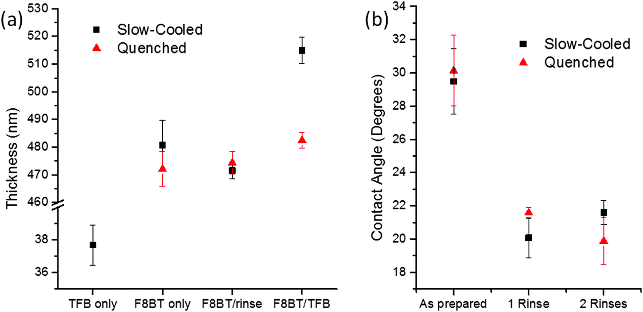 | ||
| Fig. 1 (a) Film thickness measurements of single polymer films (F8BT–TFB) and polymer bilayer films (F8BT/TFB) showing the influence of thermal and solvent processing, (b) contact angle measurement highlighting the reduction of contact angle (TFB in cyclohexanone droplets) with solvent pre-rinse. | ||
To explain these observations, the surface morphology of F8BT films following annealing and solvent treatments was analysed using atomic force microscopy (AFM). Films nominally 75 nm thick were prepared on ZnO coated glass in order to provide a realistic indication of the polymer morphology within a device structure. X-ray diffraction (XRD) studies indicate that the ZnO influences the crystallinity of F8BT deposited onto it (Fig. S2, ESI†) and this may also impact the surface. F8BT films annealed above Tm and slow-cooled to room temperature show a largely homogenous granular morphology with a surface roughness RMS of ∼2.3 nm (Fig. 2a). There is a subtle reduction in measured RMS to ∼2.0 nm following the solvent rinse with what appears to be an accompanying increase in the contrasts between areas of different heights (Fig. 2b). Also shown is the surface of the substrates on the addition of TFB (Fig. 2c). Multiple line profiles were obtained from the ZnO/F8BT (Fig. 2d) that, prior to solvent rinse, show sharp projections that are removed following the cyclohexanone rinse, this corresponds well to the reduction in the uncertainty of the thickness measurements (Fig. 1a) and the observed improvements in wetting behaviour and film quality of the bilayer. Previous reports have outlined surface features which can increase the likelihood of air pockets forming between the substrate surface and the liquid being cast with negative consequences on the wetting properties.18,19 This may explain the lack of reproducibility for TFB layer formation on F8BT films heated to only 90 °C; these films exhibit an increase in measured RMS from 1.7 to 2.5 nm after the solvent rinse, with line profiles showing a surface with sharp features (Fig. 2e) as observed in the melt processed films prior to the solvent rinse. The transition from smooth-to-rough might also explain why the TFB failed to wet the initial just-dried F8BT films that had not undergone a solvent rinse.
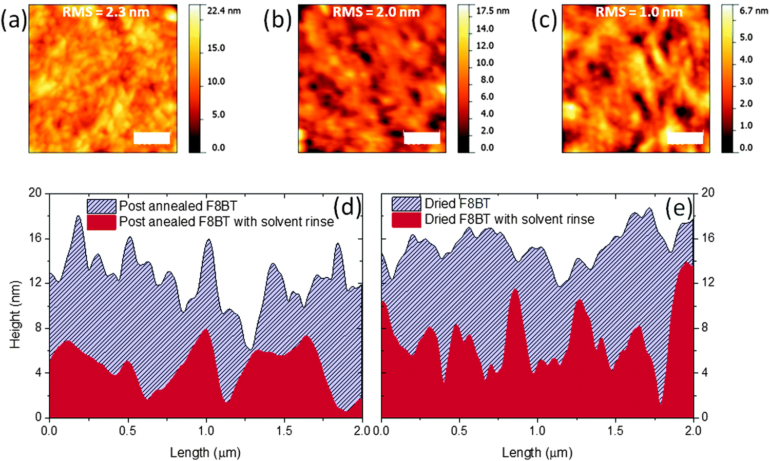 | ||
| Fig. 2 2 × 2 μm AFM images of (a) slow cooled F8BT after annealing above Tm, (b) after cyclohexanone rinse (c) following TFB addition (d and e) roughness profiles of annealed and dried at 90 °C F8BT showing the reduction in roughness observed after solvent rinse. | ||
It may be disputed whether differences in the roughness values and the length scales observed in the line profiles are too small to fully explain our experimental observations. However, the AFM and contact angle measurements suggest that thermal processing and solvent exposure influence the surface morphology of the F8BT and there is a measureable improvement in the TFB wetting. It is possible that other surface effects, such as the exposure of different functional groups brought about by changes to the polymer packing may also contribute.20 Nonetheless, for the purpose of reproducibility, all devices reported herein were fabricated using the slow-cooled F8BT subjected to a cyclohexanone spin–rinse. The structure used for all subsequent bilayer HyLED devices, ITO/ZnO (130 nm)/F8BT (75 nm)/TFB (25–100 nm)/MoO3 (15 nm)/Au (60 nm), is illustrated in Fig. 3a along with the chemical structures of F8BT and TFB. Single layer F8BT devices were also prepared where the polymer thickness was varied from 75–170 nm. Fig. S3 (ESI†) shows examples of complete bilayer devices where the TFB thickness is varied, the highly uniform films exhibiting a colour transition from green to purple as the thickness is gradually increased.
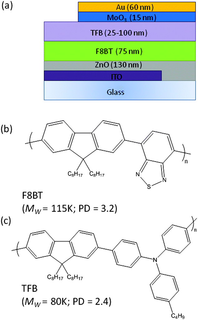 | ||
| Fig. 3 (a) Schematic illustration showing the device architecture investigated and individual layer thicknesses, (b and c) molecular structures, molecular weight (Mw) and polydispersity (PD) information for F8BT and TFB. | ||
2.2 Wavelength tuning
A significant red-shift in the device EL spectra was noticed as the TFB thickness was increased (Fig. 4a). The thinnest TFB layer (25 nm) produced EL with a maximum at 550 nm, comparable to that of F8BT-only devices, although a slightly more pronounced shoulder at 565 nm is observed in the former. At 40 nm TFB the main emission peak shifts to 575 nm, an effect that continues until it reaches 610 nm (100 nm TFB). In parallel to the main EL wavelength changing the original peak at 550 nm falls in intensity to around 50% of the main emission intensity in the thickest bilayer devices. With the bathochromic shift, the spectra also broaden, giving a range of chromaticity coordinates from (0.43, 0.56) to (0.52, 0.46), i.e. green to orange. These coordinates lie close to the locus of the Commission Internacionale d'Eclairage (CIE) plot (Fig. S4a, ESI†) indicating the highly saturated colour of the emitted spectra. As a comparison, F8BT-only devices with polymer thicknesses of 75, 90, 110 and 170 nm (comparable to the overall bilayer thicknesses) were also fabricated – these however demonstrated only subtle shifts in emission wavelength (Fig. 4b and Fig. S4b, ESI†). The observed shifts do not correlate directly with the increase in thickness as seen in the bilayer devices, for example from 90 to 110 nm there is a significant emission broadening resulting in a slight shift from yellow-green (0.46, 0.53) to yellow (0.48, 0.51), while instead the emission of the 170 nm F8BT closely resembles that of the 75 and 90 nm devices. This latter observation confirms that there is no significant self-absorption taking place within the F8BT as a consequence of increasing thickness in either device.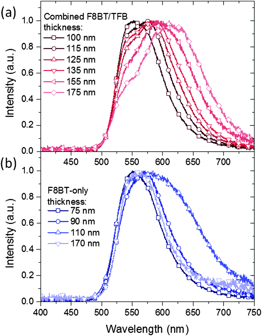 | ||
| Fig. 4 EL spectra for (a) F8BT/TFB bilayer and (b) F8BT. For bilayer devices where the TFB layer thickness is varied the F8BT layer thickness was maintained at 75 nm. | ||
We propose two possible explanations for our observations. Firstly, in the bilayer devices there is the possibility of radiative exciplex states forming close to the F8BT/TFB interface. The presence of low-energy interfacial states has been previously reported in non-inverted TFB/F8BT bilayer devices1 and may account for the lower energy emission. Variations in emission may be attributed to changes in the proportion of radiative excitons to radiative exciplex states incurred by the decreasing internal electric field. The decreasing emission from exciton states with increasing TFB thickness may then help to explain the systematic reduction to the relative intensity of the 550 nm peak. However, if this were the case, changes to the EL with respect to the forward voltage would be expected as the recombination zone shifts through the polymer region. This isn't observed and the EL remains largely the same regardless of the forward voltage (Fig. S5, ESI†). We note that the 110 nm F8BT-only device (Fig. 4b) also shows red-shifted emission, suggesting that the change is not exciplex related. Alternatively the changes in EL may be attributed to microcavity effects. In these devices a number of interfaces are present, and the large changes in refractive index (n) that result can create conditions for multiple internal reflections being possible. Such effects are well documented and have been exploited in order to maximise operating efficiencies and tune for particular emission wavelengths – typically optical spacers and semiconducting mirrors are utilised.21,22 Changes to the microcavity length i.e. from the glass/ITO interface to the MoO3/Au interface, will lead to changes in the interference of internally reflected light and would explain the changes observed in both F8BT-only and bilayer devices. There is no direct evidence from the EL spectra of emissive states due solely to transitions within the TFB layer, implying that all emission is taking place from within the F8BT layer and the near interfacial region. Therefore, with emission confined to a very specific region within the device stack, changes to the TFB thickness would induce commensurate changes to the distance between the emitting species and the reflective back contact. The observed emission wavelengths correspond to approximately four times the emitter-anode distance, hence will undergo amplified out-coupling normal to the device surface,23 these gradual physical changes then manifest as gradual changes in the EL. In the case of F8BT-only devices, changes in the EL would not be predicted to be so linearly dependent on the thickness of the emissive layer; changes to the thickness of the F8BT are accompanied with changes in the size and position of the emissive zone itself complicating the relationship with the emitter-contact distance. We therefore suggest, taking into account the proposed operating mode for HyLEDs,24 that thicker devices reposition the emission zone away from the ZnO/F8BT interface,25 but that the overall relationship between emitter-contact distance and the emission spectra is not simply linearly dependent on the emissive layer thickness.
The EL was measured ±40 degrees from the surface normal at a fixed radius for bilayer devices containing 40, 50, 60 and 100 nm of TFB. In every device the emission becomes increasingly greener with increasing viewing angle e.g. 40 nm TFB devices show a peak shift from 573 to 553 nm over the range 0 to ±40° (Fig. 5a). This corresponds to a lower extraction efficiency for shorter wavelengths at these thicknesses as the emitter-anode distance is increased beyond the quarter wavelength condition23 therefore shorter wavelengths would be trapped and likely edge emitted. Interference fringes are observed in the thickest TFB samples, highlighting the excellent quality of the interfaces present in our devices (Fig. 5d). Reflectance measurements from the gold and front electrodes also confirm the presence of weak microcavity effects.26Fig. 6 shows dips in reflection in the regions of 390 nm and 470 nm corresponding to the absorption peaks of TFB and F8BT respectively. The increase in reflectance from 500 nm onwards is the result of the back MoO3/Au contact, confirmed by obtaining reflectance through only the ITO/ZnO/F8BT/TFB layers (Fig. S6, ESI†). In the 520–560 nm region the thinner devices show a plateau in the reflectance which overlaps with the peak emission of F8BT and thus enhances the emission of these wavelengths.27 This plateau disappears as the TFB thickness increases; however, another becomes more evident in the 600–650 nm region in the thickest devices increasing the component of yellow/orange emission. Such effects are clearly observed in the F8BT-only devices, in particular, the behaviour of the 110 nm device deviates from the other three devices with a broad depression in reflectivity in the 570–650 nm corresponding to the broad, yellow EL observed. Both bilayer and F8BT-only devices share similar features i.e. those near 375, 425 and 525 nm. However when the cavity length is fixed but the composition varied i.e. a 175 nm bilayer and a 170 nm F8BT device, significant differences are observed, particularly in the 425 and 525 nm regions thus highlighting the influence of the TFB layer. These two wavelength regions coincide closely to extremes in n values of both polymers – at 410 nm for TFB n = 2.10 and for F8BT n = 1.48, however at 500 nm for TFB n = 1.80 and for F8BT n = 2.15.28 The changes in n at 425 and 525 nm may explain the features observed in Fig. 5. At 600 nm Δn is less than 0.1, thus increasing the critical angle required for total internal reflection. A greater proportion of shorter (green) wavelengths will therefore be guided to the edges of the substrates, as observed in the EL of wider viewing angles. The experimental data presented strongly suggests that the origin of the EL variations is due to the selection of different emission modes as the length of the microcavity changes.
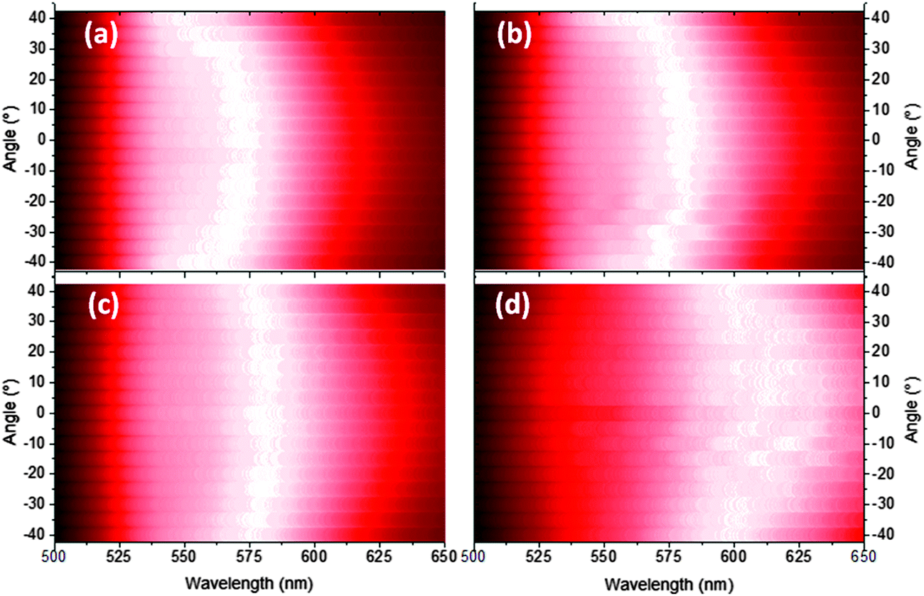 | ||
| Fig. 5 Intensity maps highlighting the shift in EL wavelength measured with changing viewing angle (±40°) for bilayer devices with a TFB thickness of (a) 40 nm, (b) 50 nm, (c) 60 nm and (d) 100 nm of TFB. | ||
 | ||
| Fig. 6 Reflectance measurements, obtained from the gold electrode, for bilayer and F8BT only devices (inset). The origin of the spectral features observed in the 550–600 nm region of both data sets may originate from microcavity effects from which the variations in device EL spectra originate. | ||
2.3 Device J–V–L and efficiency data
A minimum of two 6-pixel substrates were measured for all samples, the 25 nm TFB bilayer device was the exception, this data was obtained from one 6-pixel substrate. To prevent burnout and device degradation, bias was applied from −4 V to just above the peak of current efficiency (cd A−1). High device yields were achieved and the majority of pixels were stable to multiple test cycles, typically exhibiting an increase in light output and efficiencies between the first and second test, and stabilising thereafter. The device data presented is from the 3rd test cycle with the few devices that failed in the first or second test being excluded.The maximum current efficiencies were first determined and the current density, operating voltage, luminance and power efficiency measured at this value. Measurements were averaged giving up to 18 values for each data point. The 80 nm TFB bilayer devices, which were prepared in a separate batch owing to spatial constraints in our evaporator exhibited extremely poor yields and device performance (repeat devices showed similarly poor performance) therefore this data is obtained from the average of 2 pixels. Fig. 7 shows a peak in bilayer device efficiency and luminance with a 40 nm TFB layer and a subsequent decrease in performance as TFB thickness increases. The current required to achieve the maximum efficiency remains consistent throughout the thickness range, although there is a corresponding increase in the voltage required (13.0 to 14.7 V). A maximum current efficiency of 1.00 ± 0.08 cd A−1 was measured at 40 nm of TFB, corresponding to a luminance of 4070 ± 180 cd m−2 and a power efficiency of 0.24 ± 0.02 lm W−1. In the TFB lift-off report, Kabra et al. observe a higher current efficiency (2.81 cd A−1) for a device structure with similarly thick ZnO and MoO3 layers, but with a lower maximum luminance of 2150 cd m−2. This indicates the higher amount of current density flowing through the devices presented here does not contribute to light emission. The high current density values (J) observed in the F8BT-only devices and the significantly lower luminance values means that the bilayer devices are some 20 times more efficient than F8BT-only devices. The poor performance of the F8BT-only devices may be attributed to highly unbalanced charge transport, it is reported that HyLEDs with an energy offset to electrons at the EIL oxide/polymer electrode are strongly hole-dominated, indeed this could be further exacerbated by the thermal treatment of the F8BT for at least two reasons: (i) annealing above Tm has been reported to reduce electron mobility,20 and (ii) the improved contact between the F8BT and the underlying oxide may facilitate non-radiative exciton decay due to the deeper conduction band of the ZnO compared to the F8BT LUMO.29 Note that F8BT is known to exhibit stable behaviour and even increased photoluminescence efficiency when annealed to such temperatures;20,30 our XRD data (Fig. S2, ESI†) also shows the existence of π-stacking following the thermal procedure and as such we rule out the possibility of cross-linking or degradation which may otherwise have detrimental effects upon device performance. The role of the TFB may then be considered to balance charges in bilayer devices. TFB is an efficient hole transporter, so this effect would not be due to a redress of the charge carrier mobilities, but rather due to the approximately 0.7 eV barrier to holes as a result of the HOMO offsets (ΔHOMO) at the F8BT/TFB interface (Fig. 8a). This barrier would then limit the leakage of holes through to the ZnO and reposition the recombination zone (RZ) away from the ZnO/F8BT interface, which in itself would result in a reduction of non-radiative exciton dissociation. A shift of the RZ further into the light-emitting polymer (LEP) is also thought to occur by increasing the thickness of the LEP itself and this has been reported to lead to an increased current efficiency in HyLEDs with a Cs2CO3 interlayer at the ZnO/F8BT interface.25 However, for the F8BT-only devices here we observe a decrease between thicknesses of 75–110 nm with a slight increase at 170 nm. The current density required to achieve the maximum current efficiency decreases with increased F8BT thickness, suggesting that the devices should get more efficient. However, the observed shifts in the EL suggest that less efficient emissive modes are being selected as the total length of the micro-cavity changes – the increase in current efficiency and luminance with the 170 nm devices coincides with the EL resembling those of the thinner devices. With respect to the bilayer devices, the energetic offsets at the F8BT/TFB interface may well ensure that the recombination zone remains fixed within the F8BT layer regardless of the thickness of the TFB, possibly positioned close to the bilayer interface. The current density at maximum current efficiency remains fairly constant at around 430 mA cm−2 over the thickness range investigated; therefore changes in luminance and efficiency are a direct consequence of the changes to the microcavity length rather than repositioning of the RZ zone; the TFB is therefore acting as an optical emission tuning layer. Evidence for the effect of ΔHOMO at the F8BT/TFB interface is seen in the J–V curves before the onset of light turn-on, where following a rapid increase from 0 V the current density is seen to flat-line or, in some cases, decreases as the forward bias approaches 2 V before increasing again with voltage after light turn-on at 3.6–4 V (Fig. S7, ESI†). MoO3 is known to make an Ohmic contact with TFB and F8BT – hence holes flood the device under forward bias. These holes begin to accumulate in large numbers at the F8BT/TFB interface causing an electric field reduction across the TFB layer as the repulsion between newly injected charges and those at the interface builds (Fig. 8b). The current density would then reduce as a consequence until the voltage drop across the F8BT layer is sufficient enough to induce electron injection across the ZnO/F8BT interface whilst simultaneously enabling holes to overcome ΔHOMO (Fig. 8c). Radiative recombination ensues and the current density begins to rise with increasing forward bias. This build-up of charge is a concern as it can lead to accelerated device degradation. However, during our extensive testing no drop in luminance or efficiency was observed and no obvious difference could be discerned between the bilayer and F8BT-only devices. We note, the overall weak diode behaviour in the J–V characteristics with the current density being almost symmetrical around 0 V. Improved diode rectification (larger forward/reverse current density ratio) is observed during the first device measurements, so the increase in reverse current may be a consequence of repeat measurements. However, comparison with the J–V data of the two previously reported inverted F8BT/TFB devices shows similarly weak diode rectification suggesting that this may be an inherent characteristic in this geometry.12,13 Determining the device turn-on voltage VC is therefore non-trivial. In current HyLED literature, VC has been attributed to the energetic difference between the EIL conduction band (CB) and the emissive polymer LUMO9 as well as the differences between the metal contact work functions.31 Both of these assumptions would give VC < 1 V, which would explain the large current measured at low voltages. But, given the symmetrical nature of the J–V curves about 0 V after repeat measurements, this high current may be due to a change in the nature of interfacial states, e.g. traps, that allow for some leakage of hole current. The delay between VC and the light turn-on voltage VL may then be attributed to the period between the accumulation of charge at the interfaces and their eventual recombination in the F8BT. Such processes do not seem to have a detrimental effect on the device performance and once light turn-on was achieved the luminance was proportional to the current density across all pixels as expected. Indeed, the averaged data (Fig. 7) shows very good bilayer device consistency and reproducibility (Fig. S7, ESI†). VL was observed to be identical across all bilayer devices irrespective of TFB thickness and our values here are similar to that reported in reference 12 for F8BT/TFB HyLEDs with similarly thick ZnO and MoO3 layers. From this device sample, the respective current efficiency variation with current density was extracted showing an incredibly low efficiency roll-off across all different thicknesses of TFB (Fig. S8, ESI†). This is despite the high current densities that are generally common to HyLEDs, and further demonstrates the stability of these bilayer devices as well as the large range of operational luminances achievable without incurring significant decreases in efficiency.
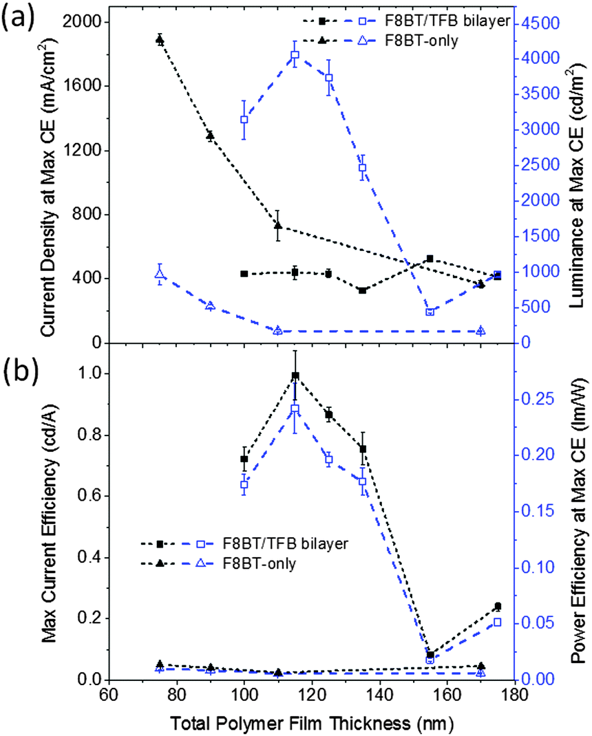 | ||
| Fig. 7 Device data for bilayer and F8BT only structures showing, (a) current density (dotted line) and luminance (dashed line) measured at maximum current efficiency (CE). (b) Maximum current efficiency (dotted line) and power efficiency at maximum current efficiency (dashed line). | ||
 | ||
| Fig. 8 (a) Flat-band energy level diagram for bilayer devices, (b) schematic illustration demonstrating, that under forward bias, the energy offset at the F8BT interface acts as a barrier to efficient carrier injection resulting in the accumulation of charge and the build up of electric fields, E(+) and E(−), that oppose the applied field EApplied, (c) the accumulated charge eventually overcomes the injection barrier – also shown is the possibility for exciplex emission if electrons successfully reach the F8BT/TFB interface. | ||
3. Conclusions
We have presented a novel and convenient route for preparing inverted architecture F8BT/TFB hybrid polymer LEDs. By identifying appropriate orthogonal solvents and thermal annealing regimes the F8BT surface has been modified to allow for successful wetting and coating by the TFB. The process is highly reproducible and significantly simpler than other processing routes proposed elsewhere. The processing route allows for inverted architecture bilayer devices to be explored, and for the role of TFB to be explored away from its conventional application as a thin interlayer. By controllably altering the TFB layer thickness we have for the first time demonstrated tuneable emission, in this case from green to orange, in inverted HyLED devices. Additionally we have demonstrated a near 20-fold increase in current efficiency compared with F8BT-only devices. We have used reflectivity and angle-dependent electroluminescence measurements to identify the formation of microcavity effects as the TFB thickness is altered; such effects highlight the high quality of the interfacial regions in our devices. The minor reduction in efficiency and luminance observed in the thickest devices are offset by the observed stability in operating current and voltage and the stability of these devices.4. Experimental
Device preparation and characterisation
ITO-coated substrates (PsiOTec, Rs ∼ 14 Ω sq−1) were cleaned via successive 15 minute ultrasonication steps using acetone, isopropanol and deionised water before a 10 minute exposure to UV-O3. ZnO layers were deposited as previously described32 then annealed for 30 minutes in a glovebox at 150 °C.33 F8BT and TFB (American Dye Source) solutions were both processed in a glovebox and passed through 0.2 μm PTFE filter prior to deposition. Both polymer layers were cast by spin-coating at 2000 rpm for 40 s. F8BT was cast from toluene at concentrations of 10 mg ml−1 for the bilayer devices, and at concentrations of 10–16 mg ml−1 for F8BT-only devices. The resulting films were annealed at just above Tm at 250 °C for fifteen minutes before being cooled slowly (5 °C min−1) back to under 100 °C. TFB layers of different thicknesses were created from solutions of concentrations between 7.5–20 mg ml−1 for the bilayer devices. The processed F8BT layers were treated with a cyclohexanone spin–rinse prior to TFB casting.17 The F8BT/TFB bilayers were dried at 130 °C for 20 minutes. F8BT-only substrates also underwent the same annealing and solvent rinse processes. Finally, MoO3 and Au were sequentially deposited via thermal evaporation at a rate of 0.1–0.3 Å s−1 and pressure of 1 × 10⁻⁶ mbar. The completed substrates were stored under an inert atmosphere until tested; all devices were measured within 48 hours of preparation. J–V and efficiency characterisation were obtained using a Keithley 236 Source Measure Unit and a Minolta luminance meter. An Ocean Optics S2000 Fibre Optic Spectrometer was attached to a purpose-built rotating holder to measure the EL at viewing angles up to 40° from the substrate surface normal.Reflectance measurements
Reflectance spectroscopy was performed after J–V–L testing using a Shimadzu 2600 UV-vis system. Reflectance measurements from the gold electrode through the device stack were made by aperturing the beam to ensure single pixel illumination. The samples were aligned such that the reflectance from the device stack excluding the MoO3/Au electrode could also be measured. A quartz baseline was used a reference and the subsequent experimental data corrected for this.Surface measurements
Surface morphology was analysed using a Vecco AFM. The effect on the wetting envelope of the solvent rinse on the thermally processed F8BT was analysed using a homemade contact angle set-up in which images were captured with a USB microscope. Contact angles were measured using the software ImageJ from captured images of TFB-cyclohexanone solution droplets on F8BT-coated glass. Thickness measurements were performed with a Veeco Dektak150 from films cast on clean glass substrates.Materials characterisation
X-ray diffraction studies were carried using a Panalytical X'Pert Pro diffractometer, operating at 40 kV and 40 mA using Ni filtered CuKα radiation. Determination of F8BT Tg and Tm was through differential scanning calorimetry with heating and cooling rates of 10 °C min−1 between 35 and 300 °C using a Mettler Toledo DSC1.Acknowledgements
J.C.D.F. is grateful for support through the EPSRC Centre for Doctoral Training in Plastic Electronics, EP/G037515/1. The authors thank Ms Kirsty A. Roy, Dr Xuhua Wang and Dr Paul N. Stavrinou for useful discussions.References
- J.-S. Kim, R. H. Friend, I. Grizzi and J. H. Burroughes, Appl. Phys. Lett., 2005, 87, 023506 CrossRef.
- J.-S. Kim, P. K. H. Ho, C. E. Murphy and R. H. Friend, Macromolecules, 2004, 37, 2861–2871 CrossRef CAS.
- T. Chiba, Y.-J. Pu, M. Hirasawa, A. Masuhara, H. Sasabe and J. Kido, ACS Appl. Mater. Interfaces, 2012, 4, 6104–6108 CAS.
- K.-H. Yim, W. J. Doherty, W. R. Salaneck, C. E. Murphy, R. H. Friend and J.-S. Kim, Nano Lett., 2010, 10, 385–392 CrossRef CAS PubMed.
- J. Bailey, E. N. Wright, X. Wang, A. B. Walker, D. D. C. Bradley and J.-S. Kim, J. Appl. Phys., 2014, 115, 204508 CrossRef.
- J. Kim, P. Ho, C. Murphy, N. Baynes and R. H. Friend, Adv. Mater., 2002, 14, 206–209 CrossRef CAS.
- J.-S. Kim, L. Lu, P. Sreearunothai, A. Seeley, K.-H. Yim, A. Petrozza, C. E. Murphy, D. Beljonne, J. Cornil and R. H. Friend, J. Am. Chem. Soc., 2008, 130, 13120–13131 CrossRef CAS PubMed.
- M. Sessolo and H. J. Bolink, Adv. Mater., 2011, 23, 1829–1845 CrossRef CAS PubMed.
- H. J. Bolink, H. Brine, E. Coronado and M. Sessolo, J. Mater. Chem., 2010, 20, 4047 RSC.
- P. de Bruyn, D. J. D. Moet and P. W. M. Blom, Org. Electron., 2012, 13, 1023–1030 CrossRef CAS.
- K. Morii, M. Ishida, T. Takashima, T. Shimoda, Q. Wang, M. K. Nazeeruddin and M. Gratzel, Appl. Phys. Lett., 2006, 89, 183510 CrossRef.
- D. Kabra, M. H. Song, B. Wenger, R. H. Friend and H. J. Snaith, Adv. Mater., 2008, 20, 3447–3452 CrossRef CAS.
- D.-Y. Chung, D.-S. Leem, D. D. C. Bradley and A. J. Campbell, Appl. Phys. Lett., 2011, 98, 103306 CrossRef.
- T.-H. Kuo, F.-C. Chen, J.-H. Li, A. T. Huang, J.-H. Huang, K.-C. Ho and C.-W. Chu, J. Mater. Chem., 2012, 22, 1364 RSC.
- J.-H. Huang, Z.-Y. Ho, T.-H. Kuo, D. Kekuda, C.-W. Chu and K.-C. Ho, J. Mater. Chem., 2009, 19, 4077 RSC.
- M. Shakutsui, H. Matsuura and K. Fujita, Org. Electron., 2009, 10, 834–842 CrossRef CAS.
- R. Trattnig, L. Pevzner, M. Jäger, R. Schlesinger, M. V. Nardi, G. Ligorio, C. Christodoulou, N. Koch, M. Baumgarten, K. Müllen and E. J. W. List, Adv. Funct. Mater., 2013, 23, 4897–4905 CrossRef CAS.
- M. Miwa, A. Nakajima, A. Fujishima, K. Hashimoto and T. Watanabe, Langmuir, 2000, 16, 5754–5760 CrossRef CAS.
- C. Ran, G. Ding, W. Liu, Y. Deng and W. Hou, Langmuir, 2008, 24, 9952–9955 CrossRef CAS PubMed.
- C. L. Donley, J. Zaumseil, J. W. Andreasen, M. M. Nielsen, H. Sirringhaus, R. H. Friend and J.-S. Kim, J. Am. Chem. Soc., 2005, 127, 12890–12899 CrossRef CAS PubMed.
- W. Brütting, J. Frischeisen, T. D. Schmidt, B. J. Scholz and C. Mayr, Phys. Status Solidi, 2013, 210, 44–65 CrossRef.
- H. Becker, S. Burns and R. Friend, Phys. Rev. B: Condens. Matter Mater. Phys., 1997, 56, 1893–1905 CrossRef CAS.
- J. Lee, N. Chopra and F. So, Appl. Phys. Lett., 2008, 92, 033303 CrossRef.
- H. J. Bolink, E. Coronado, D. Repetto, M. Sessolo, E. M. Barea, J. Bisquert, G. Garcia-Belmonte, J. Prochazka and L. Kavan, Adv. Funct. Mater., 2008, 18, 145–150 CrossRef CAS.
- D. Kabra, L. P. Lu, M. H. Song, H. J. Snaith and R. H. Friend, Adv. Mater., 2010, 22, 3194–3198 CrossRef CAS PubMed.
- V. Bulović, V. Khalfin, G. Gu, P. Burrows, D. Garbuzov and S. Forrest, Phys. Rev. B: Condens. Matter Mater. Phys., 1998, 58, 3730–3740 CrossRef.
- D. P. Puzzo, M. G. Helander, P. G. O'Brien, Z. Wang, N. Soheilnia, N. Kherani, Z. Lu and G. A. Ozin, Nano Lett., 2011, 11, 1457–1462 CrossRef CAS PubMed.
- C. M. Ramsdale and N. C. Greenham, J. Phys. D: Appl. Phys., 2003, 36, L29–L34 CrossRef CAS.
- N. Tokmoldin, PhD thesis, Imperial College Imperial, 2010.
- M. J. Banach, R. H. Friend and H. Sirringhaus, Macromolecules, 2003, 36, 2838–2844 CrossRef CAS.
- H. J. Bolink, E. Coronado, J. Orozco and M. Sessolo, Adv. Mater., 2009, 21, 79–82 CrossRef CAS.
- Y. Nakayama, K. Morii, Y. Suzuki, H. Machida, S. Kera, N. Ueno, H. Kitagawa, Y. Noguchi and H. Ishii, Adv. Funct. Mater., 2009, 19, 3746–3752 CrossRef CAS.
- M. Sessolo, H. J. Bolink, H. Brine, H. Prima-Garcia and R. Tena-Zaera, J. Mater. Chem., 2012, 22, 4916 RSC.
Footnote |
| † Electronic supplementary information (ESI) available. See DOI: 10.1039/c5tc00263j |
| This journal is © The Royal Society of Chemistry 2015 |