
 Open Access Article
 This Open Access Article is licensed under a
 Creative Commons Attribution 3.0 Unported Licence
Modulating the charge injection in organic field-effect transistors: fluorinated oligophenyl self-assembled monolayers for high work function electrodes†
Oliver
Fenwick
a,
Colin
Van Dyck‡
b,
Kathiresan
Murugavel
c,
David
Cornil
b,
Federica
Reinders
c,
Sébastien
Haar
a,
Marcel
Mayor
*cd,
Jérôme
Cornil
*b and
Paolo
Samorì
*a
aISIS & icFRC, Université de Strasbourg & CNRS, 8, allée Gaspard Monge, 67000 Strasbourg, France. E-mail: samori@unistra.fr
bLaboratory for Chemistry of Novel Materials, University of Mons, Place du Parc 20, B-7000 Mons, Belgium. E-mail: jerome.cornil@umons.ac.be
cDept. of Chemistry, University of Basel, St Johanns-Ring 19, CH-4056 Basel, Switzerland. E-mail: marcel.mayor@unibas.ch
dKarlsruhe Institute of Technology, INT, P.O. Box 3640, D-76021 Karlsruhe, Germany
First published on 10th February 2015
Abstract
The rapid increase in charge carrier mobility in organic field-effect transistors (OFETs) in the past few years, with a number of reports >10 cm2 V−1 s−1, calls for a simultaneous improvement in charge injection at the electrode–semiconductor interface. Chemical modification of the electrodes with self-assembled monolayers (SAMs) allows the optimization of three key properties for lowering the contact resistance, thus fine-tuning the charge injection into OFET channels: the electrode work function, the surface energy of the modified electrodes and tunnelling resistance of the SAM. Understanding of the interplay of these properties is of vital importance for organic device design. In this paper, we report a model study based on the modulation of all three of these properties via chemisorption of fluorinated mono- or biphenylthiol molecules (PFBT and PF2BT, respectively) onto gold electrodes. Density functional theory simulations confirm the higher work function of the PFBT monolayers compared to PF2BT and provide evidence that this work function difference is entirely due to differences in the bond dipole to the gold surface. This observation is of importance for the development of future SAM molecules both for organic electronics and across the field of surface chemistry. Incorporation of these SAM-modified Au surfaces as the source and drain electrodes of an OFET with prototypical polymer semiconductors exhibiting different transport levels makes it possible to unravel the role of energetic alignment as well as surface energy and tunnelling resistance on the device performance. Interestingly, our results show that it is not always the high work function PFBT-modified electrodes that give the lowest contact resistance.
1 Introduction
Interfaces are of critical importance in organic (opto)electronics: the device design and optimization relies on the use of interlayers to control organic–organic and organic–inorganic interfaces. In organic field-effect transistors (OFETs), optimization of charge injection and extraction at the electrode–semiconductor interface is required when targeting the fabrication of high performing devices. Such an optimization can be achieved via the control of both the wettability of the electrode to ensure favourable morphology of the semiconductor on top1,2 and its work function which needs to be matched with the semiconductor charge transport levels to reduce series (contact) resistance. Hitherto various type of interlayers have been employed for work function optimisation including polymers,3 polymer brushes,4 barium salts,5 physisorbed dendrimer monolayers,6 and chemisorbed self-assembled monolayers (SAMs),1,7,8 with the common factor between them all being that they introduce a dipole at the metal surface capable of raising or lowering its work function.In the case of chemisorbed SAMs, since the number of possible anchoring groups8–15 is limited by the chemistry of the electrode metal to which they need to bind, modification of the magnitude and direction of the surface dipole has primarily been attempted by varying the nature of the terminal moieties in the ω-position.16 Terminal groups commonly employed for decreasing electrode work functions include methyl, methoxy, sulphoxy and amino17 moieties, whilst for increasing work functions cyano8,18 and halogenated7,17,19 groups are used. For modifying gold electrodes, alkanethiols20,21 and phenylthiols22,23 are typically used as the core onto which these terminal groups are connected, where phenylthiols offer a lower tunnelling resistance due to their conjugation and typically shorter length.24
Perfluorinated monophenyl thiol (pentafluorothiophenol, PFBT)2,25–27 and its analogues with different binding groups28 are SAM forming molecules commonly utilized for increasing electrode work functions for organic devices. PFBT-modified gold electrodes, with work functions in the range of 5.5–5.8 eV,17,27,29 have shown reduced contact resistances in OFETs if compared to uncoated gold electrodes when applied in combination with a range of organic semiconductors.2,25,27 The molecular arrangement within these SAMs chemisorbed on the gold surfaces can be characterized by a number of different possible unit cells depending on the film preparation conditions, as revealed by scanning tunnelling microscopy (STM) investigations.30,31
In this paper, we decorate the surface of gold with chemisorbed SAMs of fluorinated mono or biphenylthiols in order to tune simultaneously the work function and surface energy of the electrode and exploit it for optimizing the charge injection at the electrode–semiconductor interface in OFETs when p-type polymer semiconductors with specific highest occupied molecular orbital (HOMO) levels are employed as active layers. The combination of the chosen electrode treatment with the specific polymer semiconductor enables tuning of the energetic barrier to injection from a regime of large, to moderate and even zero barrier.
Towards this end, we have designed and synthesized a biphenyl analogue of PFBT which we refer to as PF2BT (S-(2′,3′,4′,5′,6′-pentafluoro-[1,1′-biphenyl]-4-yl) ethanethioate). PF2BT incorporates an additional (non-fluorinated) phenyl group between the sulphur anchoring atom and the perfluorinated phenyl terminal moiety (Fig. 1a). Increasing the length of oligophenylthiol SAM molecules increases the intermolecular π-interactions which can aid self-assembly though at the expense of solubility. Despite identical terminal groups, differences in molecular arrangement, bond dipoles, tunnelling resistance and other molecular level properties can affect the macroscopic work function, surface energy and contact resistances in devices. By careful comparison of the structure and macroscopic properties of SAMs made of these two molecules by both experiment and simulation we show that we can fine tune the SAM properties and understand the origin of the large work function shift of gold upon functionalisation with PFBT.
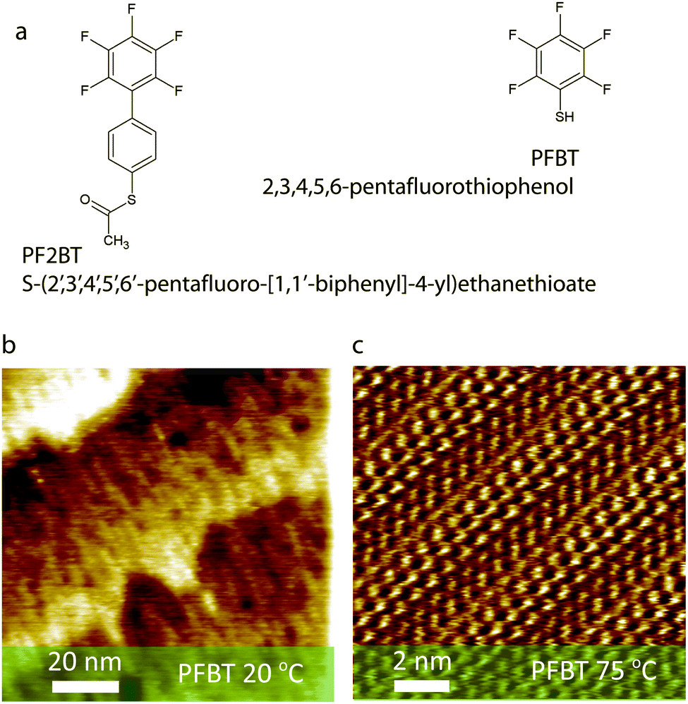 | ||
| Fig. 1 (a) Structures of the two SAM molecules used in this study. (b) STM image of partially ordered PFBT SAMs on Au(111) formed at room temperature (constant current mode, 5 pA setpoint, 200 mV bias). (c) STM of PFBT SAMs on Au(111) formed at 75 °C showing long range order (constant current mode, 6.5 pA setpoint, 20 mV bias). | ||
2 Experimental methods
2.1 Materials
2,3,4,5,6-Pentafluorothiophenol, 1-decanethiol and trichloro(octadecyl)silane were purchased from Sigma Aldrich (product numbers P5654, 705233 and 104817 respectively). Polymeric semiconducting materials were obtained commercially: P3HT (BASF, Sepiolod P200), IIDDT-C3 (1-Material, OS0402-C3), F8T2 (Sigma Aldrich, 685070). All solvents were used as received without further purification. 300 nm epitaxial Au(111) surfaces on mica were purchased from Georg Albert Physical Vapour Deposition.The synthesis of S-(2′,3′,4′,5′,6′-pentafluoro-[1,1′-biphenyl]-4-yl) ethanethioate is reported in the ESI.†
2.2 SAM preparation
Except where stated otherwise in the text, SAMs were prepared by a two hour immersion of the gold surface in a 1 mM (PFBT) or 0.5 mM (PF2BT) ethanolic solution maintained at 75 °C by an oil bath. After immersion, the samples were thoroughly rinsed with ethanol then dried with a nitrogen gun. With the exception of the transistor electrodes all gold surfaces were cleaned in with ozone (Novascan PSD-UV UV Surface Contamination System) immediately prior to immersion in the PFBT/PF2BT solutions. Note that PF2BT had limited solubility in ethanol and undissolved particles could be seen even at 0.5 mM.2.3 Water contact angle
Contact angles of sessile water drops on (functionalised) gold surfaces were measured with a Krüss DSA100 Drop Shape Analyser.2.4 Ambient photoelectron spectroscopy
The work function of SAM-modified electrodes and HOMO levels of the polymer semiconductors were measured by means of ambient photoelectron spectroscopy with a Riken Keiki spectrophotometer (Japan) model AC-2. The conditions used during the measurements were scanning energies in the range of 4.0 to 6.2 eV with a measurement interval of 0.05 eV and a UV spot intensity of 35–50 nW, to warrant a 20 meV accuracy.2.5 Scanning tunnelling microscopy
Scanning tunnelling microscopy (STM) measurements were performed using a Bruker scanning tunnelling microscope (multimode Nanoscope III, Bruker) on SAM modified gold substrates, mapping a maximum area of 1 μm × 1 μm. To increase the imaging resolution, a drop of 1-phenyloctane was added to screen the tip–sample contact from condensing water vapour. The substrates were glued onto a magnetic disk and an electric contact was made with silver paint (Aldrich Chemicals). The STM tips were mechanically cut from a Pt/Ir wire (90/10, diameter 0.25 mm). Imaging was carried out in constant current mode. The STM images were recorded at room temperature once a negligible thermal drift was achieved.2.6 Transistor fabrication
Transistors were fabricated in the bottom-gate bottom-contact configuration using pre-patterned electrodes purchased from Frauenhofer Institute for Photonic Microsystems IPMS, Dresden, Germany. The electrodes consist of 30 nm gold contact pads with a 10 nm ITO adhesion layer, patterned to have 2.5 μm, 5 μm, 10 μm or 20 μm channel lengths. The gate oxide is 230 nm SiO2, has a capacitance of 15 nF cm−2 and is supported on an n-doped silicon wafer. These electrode chips were rinsed in acetone then sonicated in acetone then isopropanol for 20 minutes in each. They were exposed to ozone for 30 minutes (Novascan PSD-UV UV Surface Contamination System) to clean the surface and remove the native HMDS layer from the gate dielectric. The chips were transferred to a nitrogen glove box and the silicon oxide surface was passivated with a trichloro(octadecyl)silane (OTS) monolayer by immersion in a 50 mM OTS solution in toluene which was then heated to 60 °C for 1 hour, before incubation for 18 hours. The chip was rinsed extensively and then spin-rinsed in toluene before functionalizing the electrodes (Section 2.2). The semiconductor was deposited by spin-coating from 0.8 wt% solutions in tetrahydrofuran (F8T2), from 4 mg mL−1 solutions in chloroform (IIDDT-C3) or drop-cast from 3 mg mL−1 solutions in chloroform (P3HT). For F8T2 and P3HT devices, the samples were subsequently annealed at 60 °C for 1 hour.2.7 Electrical testing
Electrical measurements were performed in the nitrogen atmosphere of a glove box by using a Cascade M150 probe station coupled to a Keithley 2636A sourcemeter. Contact resistances were extracted using the transfer line method based on measurements of 32 devices with channel lengths of 2.5 μm, 5 μm, 10 μm or 20 μm. Error bars represent the fitting error of the transfer line. Because of low currents in F8T2 devices we found it more practical to apply the transfer line method using the transfer curves32 rather than the output curves. Reported values and errors of the mobilities and threshold voltage are based on the mean and standard deviation of the measurements on the same 32 devices.2.8 Computational studies
To further understand the origin of the difference between the phenyl and biphenyl species, we computed the work function of the surfaces with density functional theory (DFT) calculations, using an approach which has been validated by several previous studies.7,33 The first phase of our characterization was to define an input geometry for both species. To do so, we used the STM image given in Fig. 1c. This allowed us to define a unit cell that includes six independent molecules matching both the periodicity of the gold (111) surface (with a lattice parameter of 4.08 Å34) and the unit cell parameters derived from the STM image of the PFBT SAM (Fig. 1c). Our surface unit cell has a parallelogram shape with the following parameters, which are close to the experimental ones: a = 27.509 Å; b = 5.767 Å; α = 93° (experimental parameters are aexp = 28.4 ± 2.8 Å; bexp = 6.3 ± 0.6 Å; αexp = 95.1 ± 2°). This leads to a theoretical area per molecule of about 26.3 Å2 which is in agreement with the experimental value of 30 ± 4 Å2. In view of the low resolution of STM images on the biphenyl SAM, we assumed both species to pack according to the same structural motif; thus we have in both cases employed unit cell parameters estimated experimentally by mapping by STM image of the SAM of the perfluorinated monophenylthiol.In addition to the six SAM molecules, our simulated unit cell includes five gold atomic layers and a vacuum layer (>20 Å thick) in the direction normal to the gold surface. All our calculations are done at the same level of DFT, using the LDA.CA exchange–correlation functional, a 15 × 5 × 1 Monkhorst–Pack35k-sampling and a 250 Ry mesh cut-off, as implemented in the SIESTA package.36 Core shell electrons are frozen and described by Troullier–Martins pseudopotentials and only valence electrons are explicitly treated in the Hamiltonian, described with a Double Zeta+ Polarization (DZP) numerical basis set.36,37 The agreement between the work function computed for our bare unit cell (5.21 eV, Table 1), and that tabulated for the (111) gold surface34 validates our theoretical approach.
| On polycrystalline Au | On Au(111) | From simulations | |||||
|---|---|---|---|---|---|---|---|
| θ c (°) | Φ (eV) | θ c (°) | Φ (eV) | Φ (eV) | eΔVSAM (eV) | eΔVBD (eV) | |
| a θ c = water contact angle; Φ = work function obtained by ambient UPS; eΔVSAM = work function shift achieved by a free-standing SAM layer; eΔVBD = work function shift due to bond dipole. | |||||||
| Au-only | 56.3 ± 2.2 | 4.84 ± 0.02 | 77.6 ± 0.6 | 4.93 ± 0.03 | 5.21 | — | — |
| Au/PFBT (75 °C) | 81.8 ± 0.7 | 5.63 ± 0.03 | 88.8 ± 2.6 | 5.75 ± 0.01 | 5.42 | −0.51 | +0.72 |
| Au/PF2BT (75 °C) | 95.5 ± 1.9 | 5.50 ± 0.03 | 80.6 ± 1.5 | 5.60 ± 0.02 | 5.25 | −0.49 | +0.53 |
3 Results and discussion
3.1 SAM properties
Scanning tunnelling microscopy images of PFBT based SAMs on Au(111) prepared by keeping the gold substrate in the ethanol solution at room temperature (48 hours), or at 75 °C (2 hours) are shown in Fig. 1b and c, respectively. While poorly ordered SAMs are observed for the former case, >50 nm sized two-dimensional crystalline domains have been imaged in the latter case (ESI†). Such an increase in order upon mild thermal treatment is typical of (substituted) benzenethiol SAMs on gold where, firstly, the π interactions driving assembly are not as strong as for longer oligophenylthiols30,38–41 and, secondly, gold adatoms, which are formed by relaxation of the Au(111) surface reconstruction during thiol chemisorption42,43 and inhibit the formation of large domains, can migrate to form a smaller number of larger islands when processing above about 50 °C.30,40,43,44 Ambient UPS (ESI†) estimation of the work function of PFBT functionalized Au(111) prepared at room temperature (48 hours) and at 75 °C (2 hours) amounts to 5.73 ± 0.06 eV and 5.75 ± 0.02 eV, respectively. Such similar work functions imply that the different degree of molecular order within the SAM, evidenced in Fig. 1b and c play a minor role. The work functions of the SAMs prepared at room temperature are in good accordance with previous reports of PFBT-modified electrodes.27,29 Interestingly, a small but surprising reduction in the surface energy of the lower quality SAM when compared to the higher quality one has been monitored, as evidenced by a larger water contact angle (θc).In the case of PF2BT SAMs on Au(111), a much lower work function is observed if the SAM is processed at room temperature (48 hours, ΦPF2BT,RT = 5.28 ± 0.02 eV) than when formed at 75 °C (2 hours, ΦPF2BT,75![[thin space (1/6-em)]](https://www.rsc.org/images/entities/char_2009.gif) °C = 5.60 ± 0.02 eV) (Table 1) indicating limited formation of ordered monolayers upon chemisorption at room temperature whereas upon thermal annealing a denser and more ordered monolayer is obtained. In fact, despite the increased π-interactions afforded by the extra phenyl group on the molecule, an enhanced barrier to chemisorption for thioacetates compared to analogous thiols45 combined with the low solubility of this molecule in ethanol are playing a key role. SAMs can be formed from thioacetate-containing molecules without prior deprotection, though it is documented that the SAM formation process is slower than for analogous thiols.45,46 In this case we found that an elevated temperature was needed for a SAM to form, which was confirmed by STM and by water contact angle which showed a decreased surface energy over gold immersed in ethanol without the SAM molecules.
°C = 5.60 ± 0.02 eV) (Table 1) indicating limited formation of ordered monolayers upon chemisorption at room temperature whereas upon thermal annealing a denser and more ordered monolayer is obtained. In fact, despite the increased π-interactions afforded by the extra phenyl group on the molecule, an enhanced barrier to chemisorption for thioacetates compared to analogous thiols45 combined with the low solubility of this molecule in ethanol are playing a key role. SAMs can be formed from thioacetate-containing molecules without prior deprotection, though it is documented that the SAM formation process is slower than for analogous thiols.45,46 In this case we found that an elevated temperature was needed for a SAM to form, which was confirmed by STM and by water contact angle which showed a decreased surface energy over gold immersed in ethanol without the SAM molecules.
The lower work function with respect to PFBT-functionalised gold will be discussed with the simulation results in the following section, but it is worth noting that a similar decrease in work function with increasing phenyl units is observed for gold electrodes functionalized with non-fluorinated oligophenylthiols.22
Au(111) is a good model system to use to compare our experimental results to simulations (Section 3.2), but electrodes in devices exhibit a polycrystalline gold surface. Thus it is informative to also study the macroscopic properties of these functionalized surfaces. In devices we prepared our fluorinated oligophenyl SAMs at 75 °C (2 hours) to ensure the highest quality SAMs possible. Moving from SAM-functionalised Au(111) to SAM-functionalised polycrystalline gold, there is a decrease of 0.1 eV in the work function for both PFBT and PF2BT (ESI,† Fig. S2) which can be ascribed to a less ordered SAM driven by defects in the gold surface itself. Significantly, the trend observed on Au(111) surfaces of higher work function for PFBT-functionalisation compared to PF2BT functionalisation is preserved for polycrystalline gold used for electrodes (ΔΦAu(111) = ΔΦPFBT,Au(111) − ΔΦPF2BT,Au(111) = +0.16 ± 0.02 eV; ΔΦelectrode-Au = +0.13 ± 0.04 eV).
3.2 Theoretical insight
After arranging the six independent PFBT molecules in the unit cell to mimic the experimental STM image (Fig. 1c), we optimized the geometry, minimizing the forces down to a threshold of 0.03 eV Å−1. Both the molecular layer and the adjacent two gold layers were allowed to relax in our optimization. We then simulated the STM image at the Tersoff–Hamann level of approximation,47i.e. considering that the tunnelling current is proportional to the local density of states around the gold Fermi level in a symmetric energy window chosen here to be about 0.8 eV. Comparison between the experimental and theoretical STM images, reveals a good consistency between the two images (Fig. 2e). We used the anchoring positions of the optimized packing of the PFBT system as the starting point for PF2BT before optimizing the geometry.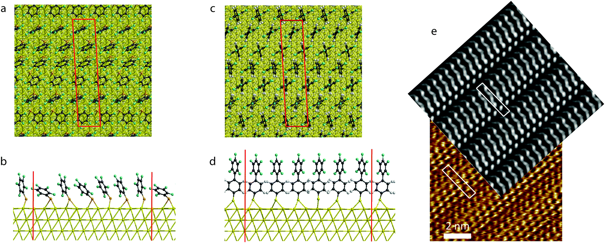 | ||
| Fig. 2 The packing of PFBT molecules on the Au(111) surface viewed (a) along the normal to the surface (b) along the short (B) axis of the unit cell. The packing of PF2BT molecules on the Au(111) surface viewed (c) along the normal to the surface (d) along the short (B) axis of the unit cell. Red boxes and lines mark the unit cell boundaries. (e) Comparison between the simulated (overlay) and measured (underlay) STM images for the PFBT SAM on gold. White boxes indicate the unit cell boundaries. The bright spots are located at the topmost fluorine atoms. Measured STM image was recorded in constant current mode using a 6.5 pA setpoint and a 20 mV bias. | ||
Despite the same unit cell dimensions and very similar anchoring positions of the molecules in the PFBT and PF2BT SAMs, the geometric arrangement of molecules is quite different in each case. We attribute this to the repulsion between the fluorine atoms (which have a large van der Waals radius) on the terminal phenyl unit (steric effect). The shorter PFBT molecules can explore a large range of tilt angles whilst keeping the fluorinated units at a reasonable distance, with some molecules finding an energy minimum at tilt angles >45°. On the other hand, PF2BT SAMs have the same area per molecule but the greater length of those molecules means that they cannot explore such a wide range of tilt angles without feeling the steric hindrance. As a result, all molecules in the PF2BT SAM adopt orientations normal to the surface and their terminal (fluorinated) phenyl units orient in the same direction within the plane. These significant differences in molecular ordering are likely to have an impact on the SAM work functions.
After solving the DFT equations, we get access to the electrostatic potential at each point of the unit cell. This allows us to average this latter quantity along the planes parallel to the gold surface and to create an electrostatic profile along the z direction normal to the surface. After setting the zero of energy to the Fermi level of the system, the work function is directly readable from the profile value in the vacuum area. Such profiles are reported in Fig. 3, showing a work function of 5.42 eV in the PFBT case and 5.25 eV in the PF2BT case. This corresponds to an upward shift of the work function in both cases compared to the bare gold surface, in agreement with experimental measurements. Furthermore, the calculation of a work function higher by 0.17 eV for the PFBT system compared to the PF2BT system is also in very good quantitative agreement with the experiments (0.15 ± 0.02 eV). However, our computed work functions for the defect-free covered electrodes are about 0.3 eV lower in absolute terms than the experiments, which is something that we have observed previously when comparing our modelling to experimentally-measured work functions.7,48 We also stress that that we do not consider differences between the experimental (4.93 ± 0.03 eV) and theoretical values (5.21 eV) of the gold work function to be problematic since the UPS measurements were done in air where the gold surface is likely to become contaminated soon after cleaning, which will reduce its work function to values lower than that of pristine Au(111) surfaces. Nevertheless, our calculation grasps the variation in the work function between the two gold–SAM systems.
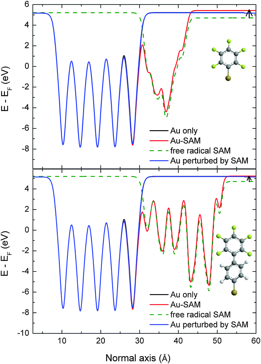 | ||
| Fig. 3 Electrostatic potential profiles averaged in the planes parallel to the normal axis for (top) PFBT-modified gold surfaces and (bottom) PF2BT-modified gold surfaces. The black lines are the profiles of the free unperturbed gold surfaces. This perfectly matches the blue curves, representing the gold surface for which the geometry has been perturbed by the SAM deposition, thus implying that this geometry relaxation does not affect the work function shift. The electrostatic potentials of the full systems are given in red; the difference with the blue and black lines in the vacuum region directly gives the work function shift upon SAM deposition. The green dashed lines represent the potential of the free radical SAM, which reveals the work function shift that would be observed in the absence of any interaction between the electrode and the monolayer. The small black arrows between the red and green lines on the right hand side show the bond dipole contribution to the work function shift. | ||
We can further analyze the origin of this difference in work functions of the two SAM-modified surfaces by decomposing the shift of the work function into two contributions. The origin of the work function shift, ΔΦ, is the surface dipole which arises both from the intrinsic dipole of the molecules in the SAM layer (ΔVSAM) and the dipole created as the thiol anchoring groups bind to the gold surface (BD):
| ΔΦ = ΔVSAM + BD |
The free SAM profiles show that the intrinsic contributions, ΔVSAM, lead to a downward shift of the work function by about −0.51 eV for the phenyl and −0.49 eV for the biphenyl. Thus, the incorporation of an additional phenyl unit into the SAM molecule does not significantly affect the intrinsic dipole moment of the SAM. Surprisingly, for PFBT SAMs, we note that different geometric organization of the SAM molecules obtained during optimization had little impact on ΔVSAM which varied by only 6.5%, which may explain our observation of similar work functions for ordered and disordered PFBT SAMs in Section 3.1. On the other hand, the bond dipole, BD, contributions are +0.72 eV for PFBT SAMs and +0.53 eV for the PF2BT SAMs. We then conclude that the small difference in work function between the PFBT and PF2BT SAMs is only due to the charge reorganization at the metal/SAM interface. This rationalizes both the small experimental difference in work function between the two systems, and the reason for the slightly lower work function in the case of PF2BT.
3.3 SAMs in devices
To test our SAMs in transistors, we used a bottom gate bottom contact configuration and as active layer we selected three polymeric p-type semiconductors with three distinct HOMO levels (Fig. 4a). In particular, the HOMO level for P3HT (−4.86 ± 0.02 eV) lies at the same energy as the Fermi level of gold and therefore offers no energetic barrier to hole injection from either the bare gold or from the PFBT/PF2BT-functionalised gold electrodes. On the other hand, IIDDT-C3 (HOMOIIDDT-C3 = −5.34 ± 0.02 eV) has an energetic barrier for injection from bare gold electrodes but not from the functionalized electrodes, whilst F8T2 (HOMOF8T2 = −5.55 ± 0.02 eV) has an energetic barrier to injection from bare gold and PF2BT-functionalised electrodes but not from the PFBT-functionalised ones. In this way, we are able explore a wide range of combinations of the work function of the electrodes with the HOMO of the polymers to study the effect of energy level alignment on the contact resistance in the context of other effects such as SAM tunnelling resistance and morphological effects due to changes in the electrode surface energy.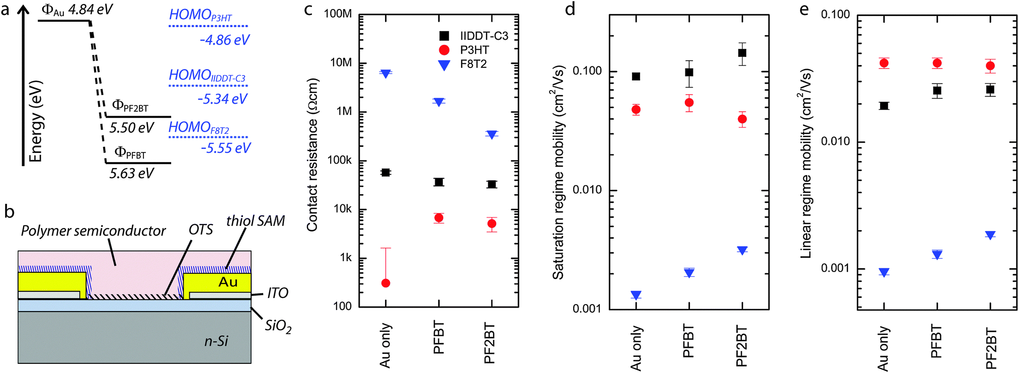 | ||
| Fig. 4 (a) Energy levels of the (modified) electrodes and the polymer semiconductors. (b) Schematic of the OFET structure. (c) Contact resistance, (d) saturation regime mobility and (e) linear regime mobility of the devices made with gold or SAM-modified electrodes and the three semiconducting polymers IIDDT-C3 (black squares), P3HT (red circles) and F8T2 (blue triangles). | ||
In the case of P3HT, the contact resistances are very small when using all types of (functionalized) electrodes and is essentially zero in the case of gold contacts (Rc,Au = 0.3 ± 1.3 kΩ cm). This result, which can be explained in view of the absence of an energetic injection barrier (Table 1 and Fig. 4a), is consistent with previous reports on devices based on a similar geometry.49 On the other hand, a small contact resistance has been measured for both PFBT- and PF2BT-functionalised electrodes (6.8 ± 1.5 kΩ cm and 5.2 ± 1.7 kΩ cm, respectively), indicating that the energetics are not the only factors playing a role. In fact there are two other effects that should be considered: (i) the surface energy of the functionalized electrode which can locally influence the semiconductor morphology and affect the transport in the short distance through the semiconductor bulk to the accumulation layer;50,51 and (ii) the electrical tunnelling resistance of the SAM layer.19,52,53 The indistinguishable contact resistances between the PFBT and PF2BT devices and the similarity of their terminal groups suggest that the semiconductor morphology might be playing the dominant role in this small contact resistance. This interpretation is partly supported by the water contact angle measurements showing in both cases values which are much larger than for bare gold (Table 1), though with slightly larger water contact angles for PF2BT than for PFBT. Meanwhile, the simulation predicts that the biphenyl molecules have a greater tendency to adopt an upright orientation (Fig. 2d), which combined with the greater molecular length implies that the biphenyl SAM is much thicker than the monophenyl SAM. A higher water contact angle in the PF2BT case introduces the possibility of increased crystallinity and higher mobility of the semiconductor near the electrode, whilst a thicker PF2BT SAM would exhibit larger tunnelling resistances than PFBT SAMs; these opposing effects may explain the similarity in contact resistance between PFBT and PF2BT-treated electrodes. It should also be noted that similar contact resistances for conjugated SAMs of different thicknesses can be explained by the modest tunnelling beta value being much lower in the case of oligophenylthiols (∼0.3–0.4 Å−1)24,54 than for non-conjugated SAMs such as alkanethiols.24,53,55 The field-effect mobilities for these devices (not corrected for the contact resistance) amount to 0.04–0.05 cm2 V−1 s−1 with no measureable influence of the contact resistance due to its small value in comparison to the relatively large channel resistance.
In the case of IIDDT-C356 transistors, the contact resistance is about 60% higher for gold electrodes (57.3 ± 4.5 kΩ cm) than for the SAM-treated electrodes (37.1 ± 6.5 kΩ cm and 32.9 ± 5.1 kΩ cm for PFBT and PF2BT respectively). Correspondingly, mobilities calculated without compensating for the contact resistances are slightly lower in the case of bare gold electrodes than for the devices with SAM-functionalised electrodes (Table 2). This is consistent with the energetic barrier for injection playing a role in this case, since the energetic barrier for injection from gold should be finite (∼0.35 eV), whereas for the SAM-functionalised electrodes, which have higher work functions, there is no energetic barrier to injection (Table 1).
| μ sat (cm2 V−1 s−1) | μ lin (cm2 V−1 s−1) | V t (V) | R c (kΩ cm) | ||
|---|---|---|---|---|---|
| a μ sat = field-effect mobility in the saturation regime; μlin = field-effect mobility in the linear regime; Vt = threshold voltage; Rc = contact resistance determined from the transfer line method. | |||||
| P3HT | Au-only | (4.8 ± 0.5) × 10−2 | 0.042 ± 0.004 | −5.4 ± 1.3 | 0.3 ± 1.3 |
| Au/PFBT | (5.5 ± 0.9) × 10−2 | 0.042 ± 0.004 | −2.6 ± 2.3 | 6.8 ± 1.5 | |
| Au/PF2BT | (4.0 ± 0.6) × 10−2 | 0.040 ± 0.005 | −4.5 ± 0.8 | 5.2 ± 1.7 | |
| IIDDT-C3 | Au-only | (0.91 ± 0.05) × 10−1 | 0.019 ± 0.001 | −16.6 ± 1.2 | 57.3 ± 4.5 |
| Au/PFBT | (0.99 ± 0.05) × 10−1 | 0.026 ± 0.003 | −10.7 ± 1.2 | 37.1 ± 6.5 | |
| Au/PF2BT | (1.4 ± 0. 3) × 10−1 | 0.026 ± 0.003 | −11.9 ± 1.6 | 32.9 ± 5.1 | |
| F8T2 | Au-only | (1.3 ± 0.1) × 10−3 | (0.95 ± 0.05) × 10−3 | −17.8 ± 0.4 | (6.3 ± 0.3) × 103 |
| Au/PFBT | (2.1 ± 0.2) × 10−3 | (1.3 ± 0.1) × 10−3 | −16.4 ± 0.3 | (2.1 ± 0.3) × 103 | |
| Au/PF2BT | (3.2 ± 0.1) × 10−3 | (1.2 ± 0.1) × 10−3 | −16.5 ± 0.5 | (0.59 ± 0.11) × 103 | |
Finally, in the case of F8T2, all contact resistances are very high, possibly due to the lower mobility of the semiconductor which we did not anneal to avoid damaging the SAMs. We see by far the largest contact resistance from the bare gold electrodes (6.3 ± 0.3 MΩ cm) much in line with values reported previously in the literature.49 This resistance is reduced for SAM-treated electrodes, with the contact resistance of the PF2BT devices (0.59 ± 0.11 MΩ cm) being significantly lower than for PFBT devices (2.1 ± 0.3 MΩ cm). The very large contact resistance for injection from gold electrodes is in full agreement with our energetic picture (Fig. 4a and Table 1) which shows a large (>0.5 eV) energetic barrier for hole injection. Despite the expected lower contact resistances for SAM-modified electrodes, a larger contact resistance for PFBT-modified electrodes when compared to PF2BT-modified electrodes is surprising considering the absence of an energetic barrier to injection for PFBT-modified electrodes but a small (0.05 eV) barrier to injection for PF2BT-modified electrodes. The origin of this could lie in the different surface energies revealed by the slightly higher water contact angle for PF2BT-functionalised polycrystalline gold, but there are also properties peculiar to F8T2 devices that need to be considered. F8T2 exhibits a particularly large and stable bias stress effect whose origins lie in trapped space-charge57 and the formation of stable bipolaron species;58 this has been shown to have a large detrimental effect on the contact resistance near the source electrode,57 with the effect amplified when a bottom-gate bottom-contact geometry like ours is employed. The literature also confirms our observation of contact resistances in the region of several MΩ cm in our geometry (for bare gold electrodes).57 In fact, in the case of PFBT-treated electrodes, charge transfer from the source and drain to F8T2 due to electrode work function pinning could increase the space charge in the vicinity of the electrodes before device operation and increase the contact resistance compared to PF2BT-treated electrodes where there should be no electrode work function pinning. Whichever of the two explanations underpins our observation, we are able to show improved device performance for PF2BT-treated electrodes over PFBT-treated electrodes.
4. Conclusions
In summary, we have studied SAMs on gold formed from two perfluorinated mono- and biphenylthiol compounds, i.e. PFBT and PF2BT. Both SAMs induce a large increase in the gold work function, which is slightly larger for the monophenyl PFBT SAMs (5.75 eV) than for the biphenyl PF2BT SAMs (5.60 eV). Numerical simulations show that, although free-standing monolayers of the two molecules have almost identical dipoles, there is a large difference in the bond dipole of the SAM to the gold surface. This difference in bond dipole is proven to be the only reason for the larger work function of PFBT-modified gold surfaces and this finding highlights the importance of considering the bond dipole when designing future SAM molecules for work function modification.The use of these SAMs on Au electrodes of OFETs in combination with the use of three prototypical polymeric semiconductors with different HOMO levels, made it possible to elucidate the effect of electrode functionalisation on changes in the contact resistance. Despite observing effects caused by tunnelling resistance and surface energy, the electrode work function dominated the tuning of contact resistance. In all cases, devices incorporating PF2BT-functionalised electrodes showed contact resistances that were equal to or lower than those incorporating PFBT-functionalised electrodes, demonstrating our new biphenyl molecule, PF2BT, to be a good choice for improving injection in OFETs.
Acknowledgements
The authors would like to thank Prof. Franco Cacialli for useful discussions. Financial support from the ERC project SUPRAFUNCTION (GA-257305), the EC Marie-Curie projects IEF-MULTITUDES (PIEF-GA-2012-326666) and ITN iSwitch (GA no. 642196), the Agence Nationale de la Recherche through the LabEx project Chemistry of Complex Systems (ANR-10-LABX-0026_CSC), and the International Center for Frontier Research in Chemistry (icFRC). The computational work was supported by the Interuniversity Attraction Pole Programme (P7/05) initiated by the Belgian Science Policy Office, and by the Belgian National Fund for Scientific Research (FNRS). J.C. is an FNRS research director. Colin Van Dyck is a recipient of a Gustave Boël – Sofina Fellowship of the Belgian American Educational Foundation (BAEF). K.M., F.R. and M.M. acknowledge financial support by the Swiss National Science Foundation (SNF) and the Swiss Nanoscience Institute (SNI).Notes and references
- J. Kim, Y. S. Rim, Y. S. Liu, A. C. Serino, J. C. Thomas, H. J. Chen, Y. Yang and P. S. Weiss, Nano Lett., 2014, 14, 2946–2951 CrossRef CAS PubMed.
- S. K. Park, D. A. Mourey, S. Subramanian, J. E. Anthony and T. N. Jackson, Appl. Phys. Lett., 2008, 93, 043301 CrossRef PubMed.
- Y. H. Zhou, C. Fuentes-Hernandez, J. Shim, J. Meyer, A. J. Giordano, H. Li, P. Winget, T. Papadopoulos, H. Cheun, J. Kim, M. Fenoll, A. Dindar, W. Haske, E. Najafabadi, T. M. Khan, H. Sojoudi, S. Barlow, S. Graham, J. L. Brédas, S. R. Marder, A. Kahn and B. Kippelen, Science, 2012, 336, 327–332 CrossRef CAS PubMed.
- E. Schwartz, E. Lim, C. M. Gowda, A. Liscio, O. Fenwick, G. Tu, V. Palermo, R. de Gelder, J. J. L. M. Cornelissen, E. R. H. Van Eck, A. P. M. Kentgens, F. Cacialli, R. J. M. Nolte, P. Samorì, W. T. S. Huck and A. E. Rowan, Chem. Mater., 2010, 22, 2597–2607 CrossRef CAS.
- N.-K. Kim, D. Khim, Y. Xu, S.-H. Lee, M. Kang, J. Kim, A. Facchetti, Y.-Y. Noh and D.-Y. Kim, ACS Appl. Mater. Interfaces, 2014, 6, 9614–9621 CAS.
- G. Winroth, O. Fenwick, M. A. Scott, D. Yip, S. Howorka and F. Cacialli, Appl. Phys. Lett., 2010, 97, 043304 CrossRef PubMed.
- N. Crivillers, S. Osella, C. Van Dyck, G. M. Lazzerini, D. Cornil, A. Liscio, F. Di Stasio, S. Mian, O. Fenwick, F. Reinders, M. Neuburger, E. Treossi, M. Mayor, V. Palermo, F. Cacialli, J. Cornil and P. Samorì, Adv. Mater., 2013, 25, 432–436 CrossRef CAS PubMed.
- F. Rissner, G. M. Rangger, O. T. Hofmann, A. M. Track, G. Heimel and E. Zojer, ACS Nano, 2009, 3, 3513–3520 CrossRef CAS PubMed.
- L. V. Protsailo, W. R. Fawcett, D. Russell and R. L. Meyer, Langmuir, 2002, 18, 9342–9349 CrossRef CAS.
- J. N. Hohman, J. C. Thomas, Y. Zhao, H. Auluck, M. Kim, W. Vijselaar, S. Kommeren, A. Terfort and P. S. Weiss, J. Am. Chem. Soc., 2014, 136, 8110–8121 CrossRef CAS PubMed.
- C. M. Crudden, J. H. Horton, I. I. Ebralidze, O. V. Zenkina, A. B. McLean, B. Drevniok, Z. She, H.-B. Kraatz, N. J. Mosey, T. Seki, E. C. Keske, J. D. Leake, A. Rousina-Webb and G. Wu, Nat. Chem., 2014, 6, 409–414 CrossRef CAS PubMed.
- L. Piot, C. Marie, X. Dou, X. Feng, K. Mullen and D. Fichou, J. Am. Chem. Soc., 2009, 131, 1378 CrossRef CAS PubMed.
- M. Cavallini, M. Bracali, G. Aloisi and R. Guidelli, Langmuir, 1999, 15, 3003–3006 CrossRef CAS.
- M. Delalande, S. Clavaguera, M. Toure, A. Carella, S. Lenfant, D. Deresmes, D. Vuillaume and J. P. Simonato, Chem. Commun., 2011, 47, 6048–6050 RSC.
- Y. F. Wang, O. Zeiri, L. Meshi, F. Stellacci and I. A. Weinstock, Chem. Commun., 2012, 48, 9765–9767 RSC.
- D. Cornil and J. Cornil, J. Electron Spectrosc. Relat. Phenom., 2013, 189, 32–38 CrossRef CAS PubMed.
- Y. Kuzumoto and M. Kitamura, Appl. Phys. Express, 2014, 7, 035701 CrossRef.
- D. Brete, D. Przyrembel, C. Eickhoff, R. Carley, W. Freyer, K. Reuter, C. Gahl and M. Weinelt, J. Phys.: Condens. Matter, 2012, 24, 394015 CrossRef PubMed.
- X. Cheng, Y.-Y. Noh, J. Wang, M. Tello, J. Frisch, R.-P. Blum, A. Vollmer, J. P. Rabe, N. Koch and H. Sirringhaus, Adv. Funct. Mater., 2009, 19, 2407–2415 CrossRef CAS.
- K. Asadi, F. Gholamrezaie, E. C. P. Smits, P. W. M. Blom and B. d. Boer, J. Mater. Chem., 2007, 17, 1947–1953 RSC.
- P. Stoliar, R. Kshirsagar, M. Massi, P. Annibale, C. Albonetti, D. M. de Leeuw and F. Biscarini, J. Am. Chem. Soc., 2007, 129, 6477–6484 CrossRef CAS PubMed.
- E. Orgiu, N. Crivillers, J. Rotzler, M. Mayor and P. Samorì, J. Mater. Chem., 2010, 20, 10798–10800 RSC.
- D. Boudinet, M. Benwadih, Y. B. Qi, S. Altazin, J. M. Verilhac, M. Kroger, C. Serbutoviez, R. Gwoziecki, R. Coppard, G. Le Blevennec, A. Kahn and G. Horowitz, Org. Electron., 2010, 11, 227–237 CrossRef CAS PubMed.
- D. J. Wold, R. Haag, M. A. Rampi and C. D. Frisbie, J. Phys. Chem. B, 2002, 106, 2813–2816 CrossRef CAS.
- R. Hamilton, J. Smith, S. Ogier, M. Heeney, J. E. Anthony, I. McCulloch, J. Veres, D. D. C. Bradley and T. D. Anthopoulos, Adv. Mater., 2009, 21, 1166–1171 CrossRef CAS.
- J.-P. Hong, A.-Y. Park, S. Lee, J. Kang, N. Shin and D. Y. Yoon, Appl. Phys. Lett., 2008, 92, 143311 CrossRef PubMed.
- J. Smith, R. Hamilton, Y. Qi, A. Kahn, D. D. C. Bradley, M. Heeney, I. McCulloch and T. D. Anthopoulos, Adv. Funct. Mater., 2010, 20, 2330–2337 CrossRef CAS.
- B. A. MacLeod, N. E. Horwitz, E. L. Ratcliff, J. L. Jenkins, N. R. Armstrong, A. J. Giordano, P. J. Hotchkiss, S. R. Marder, C. T. Campbell and D. S. Ginger, J. Phys. Chem. Lett., 2012, 3, 1202–1207 CrossRef CAS.
- H. Lee, Y. Zhang, L. Zhang, T. Mirabito, E. K. Burnett, S. Trahan, A. R. Mohebbi, S. C. B. Mannsfeld, F. Wudl and A. L. Briseno, J. Mater. Chem. C, 2014, 2, 3361–3366 RSC.
- H. Kang, N. S. Lee, E. Ito, M. Hara and J. Noh, Langmuir, 2010, 26, 2983–2985 CrossRef CAS PubMed.
- W. Azzam, A. Bashir, P. U. Biedermann and M. Rohwerder, Langmuir, 2012, 28, 10192–10208 CrossRef CAS PubMed.
- T. Leydecker, D. Trong Duong, A. Salleo, E. Orgiu and P. Samorì, ACS Appl. Mater. Interfaces, 2014, 6, 21248–21255 CAS.
- N. Crivillers, A. Liscio, F. Di Stasio, C. Van Dyck, S. Osella, D. Cornil, S. Mian, G. M. Lazzerini, O. Fenwick, E. Orgiu, F. Reinders, S. Braun, M. Fahlman, M. Mayor, J. Cornil, V. Palermo, F. Cacialli and P. Samorì, Phys. Chem. Chem. Phys., 2011, 13, 14302–14310 RSC.
- D. R. Lide, CRC Handbook of Chemistry and Physics, Taylor & Francis, 2004 Search PubMed.
- H. J. Monkhorst and J. D. Pack, Phys. Rev. B: Solid State, 1976, 13, 5188–5192 CrossRef.
- E. Artacho, E. Anglada, O. Diéguez, J. D. Gale, A. García, J. Junquera, R. M. Martin, P. Ordejón, J. M. Pruneda, D. Sánchez-Portal and J. M. Soler, J. Phys.: Condens. Matter, 2008, 20, 064208 CrossRef PubMed.
- J. Junquera, Ó. Paz, D. Sánchez-Portal and E. Artacho, Phys. Rev. B: Condens. Matter Mater. Phys., 2001, 64, 235111 CrossRef.
- A.-A. Dhirani, R. W. Zehner, R. P. Hsung, P. Guyot-Sionnest and L. R. Sita, J. Am. Chem. Soc., 1996, 118, 3319–3320 CrossRef CAS.
- Y.-T. Tao, C.-C. Wu, J.-Y. Eu, W.-L. Lin, K.-C. Wu and C.-h. Chen, Langmuir, 1997, 13, 4018–4023 CrossRef CAS.
- H. Kang, T. Park, I. Choi, Y. Lee, E. Ito, M. Hara and J. Noh, Ultramicroscopy, 2009, 109, 1011–1014 CrossRef CAS PubMed.
- H. Kang, D. Lee, E. Ito, J. B. Park, M. Hara and J. Noh, J. Nanosci. Nanotechnol., 2014, 14, 5054–5058 CrossRef CAS PubMed.
- G. E. Poirier, Langmuir, 1997, 13, 2019–2026 CrossRef CAS.
- G. Yang and G.-y. Liu, J. Phys. Chem. B, 2003, 107, 8746–8759 CrossRef CAS.
- R. Yamada, H. Wano and K. Uosaki, Langmuir, 2000, 16, 5523–5525 CrossRef CAS.
- M. I. Béthencourt, L. Srisombat, P. Chinwangso and T. R. Lee, Langmuir, 2009, 25, 1265–1271 CrossRef PubMed.
- Y. K. Kang, D. J. Won, S. R. Kim, K. J. Seo, H. S. Choi, G. H. Lee, Z. S. Noh, T. S. Lee and C. J. Lee, Mater. Sci. Eng., C: Biomimetic Supramol. Syst., 2004, 24, 43–46 CrossRef PubMed.
- J. Tersoff and D. R. Hamann, Phys. Rev. Lett., 1983, 50, 1998–2001 CrossRef CAS.
- A. M. Masillamani, S. Osella, A. Liscio, O. Fenwick, F. Reinders, M. Mayor, V. Palermo, J. Cornil and P. Samorì, Nanoscale, 2014, 6, 8969–8977 RSC.
- L. Bürgi, T. J. Richards, R. H. Friend and H. Sirringhaus, J. Appl. Phys., 2003, 94, 6129–6137 CrossRef PubMed.
- R. Li, J. W. Ward, D.-M. Smilgies, M. M. Payne, J. E. Anthony, O. D. Jurchescu and A. Amassian, Adv. Mater., 2012, 24, 5553–5558 CrossRef CAS PubMed.
- W. S. Hu, Y. T. Tao, Y. J. Hsu, D. H. Wei and Y. S. Wu, Langmuir, 2005, 21, 2260–2266 CrossRef CAS PubMed.
- C. Liu, Y. Xu and Y.-Y. Noh, Mater. Today, 2015, 18, 79–96 CrossRef CAS PubMed.
- M. M. Thuo, W. F. Reus, C. A. Nijhuis, J. R. Barber, C. Kim, M. D. Schulz and G. M. Whitesides, J. Am. Chem. Soc., 2011, 133, 2962–2975 CrossRef CAS PubMed.
- A. M. Masillamani, N. Crivillers, E. Orgiu, J. Rotzler, D. Bossert, R. Thippeswamy, M. Zharnikov, M. Mayor and P. Samorì, Chem. – Eur. J., 2012, 18, 10335–10347 CrossRef CAS PubMed.
- C. Boulas, J. V. Davidovits, F. Rondelez and D. Vuillaume, Phys. Rev. Lett., 1996, 76, 4797–4800 CrossRef CAS.
- T. Lei, J.-H. Dou and J. Pei, Adv. Mater., 2012, 24, 6457–6461 CrossRef CAS PubMed.
- T. Richards and H. Sirringhaus, Appl. Phys. Lett., 2008, 92, 023512 CrossRef PubMed.
- R. A. Street, A. Salleo and M. L. Chabinyc, Phys. Rev. B: Condens. Matter Mater. Phys., 2003, 68, 085316 CrossRef.
Footnotes |
| † Electronic supplementary information (ESI) available: Synthesis of PF2BT, ambient photoelectron spectroscopy data, water contact angle data. See DOI: 10.1039/c5tc00243e |
| ‡ Present address: Department of Chemistry, Northwestern University, 2145 Sheridan Road, Evanston, Illinois 60208, USA. |
| This journal is © The Royal Society of Chemistry 2015 |