
 Open Access Article
 This Open Access Article is licensed under a
 Creative Commons Attribution 3.0 Unported Licence
Polytellurophenes provide imaging contrast towards unravelling the structure–property–function relationships in semiconductor:insulator polymer blends†
Ashlee A.
Jahnke
a,
Liyang
Yu
bc,
Neil
Coombs
a,
Alberto D.
Scaccabarozzi
b,
Andrew J.
Tilley
a,
Paul M.
DiCarmine
a,
Aram
Amassian
c,
Natalie
Stingelin
*b and
Dwight S.
Seferos
*a
aDepartment of Chemistry, University of Toronto, Toronto, Ontario M5S 2P5, Canada. E-mail: dseferos@chem.utoronto.ca
bDepartment of Materials and Centre for Plastic Electronics, Imperial College London, London SW7 2AZ, UK. E-mail: n.stingelin-stutzmann@imperial.ac.uk
cDepartment of Materials Science and Engineering, King Abdullah University of Science and Technology, Thuwal, Kingdom of Saudi Arabia
First published on 27th February 2015
Abstract
Polymer blends are broadly important in chemical science and chemical engineering and have led to a wide range of commercial products, however their precise structure and phase morphology is often not well understood. Here we show for the first time that π-conjugated polytellurophenes and high-density polyethylene form blends that can serve as active layers in field-effect transistor devices and can be characterized by a variety of element-specific imaging techniques such as STEM and EDX. Changing the hydrocarbon content and degree of branching on the polytellurophene side-chain leads to a variety of blend structures, and these variations can be readily visualized. Characterization by electron microscopy is complemented by topographic and X-ray methods to establish a nano- to micro-scale picture of these systems. We find that blends that possess microscale networks function best as electronic devices; however, contrary to previous notions a strong correlation between nanofiber formation and electrical performance is not observed. Our work demonstrates that use of organometallic polymers assists in clarifying relevant structure–property–function relationships in multicomponent systems such as semiconductor:insulator blends and sheds light on the structure development in polymer:polymer blends including crystallization, phase separation, and formation of supramolecular arrangements.
Introduction
Polymer composites and blends are technologically important and found in products ranging from car bumpers to electronics and biomedical devices. Within such multicomponent systems, the individual components can be highly immiscible, especially when they are macromolecules, resulting in some degree of phase separation with significant impact on material properties and functionality. Typically a polymer is combined with an inorganic or organic component of nano- to macro-scale dimensions such as exfoliated clay,1 carbon nanotubes,2–4 nanofibers,5 graphene,6 or nanocrystalline metals.7,8 These composites have attracted significant attention due to their advantageous mechanical properties9 where the guest component is used to increase the modulus and/or stiffness of the macromolecular matrix. Composites have also been used to improve barrier properties,10,11 flammability resistance,12,13 blend compatibilization,14,15 and electrical conductivity.16,17 Because of the drastically different chemical and/or physical-chemical nature of the constituting components of such composites, structure analysis is usually relatively straightforward. In contrast, it is significantly more challenging to obtain a structural picture of polymer:polymer blends, because of broad similarities in elemental composition of the components. In the case of semiconducting:insulating polymer blends, which offer an often desirable combination of properties, e.g. good electronic characteristics as well as mechanical robustness,18,19 structural characterization can be highly challenging. Indeed, as is the case with most insulator:insulator blends, the phase morphology and solid-state microstructure can be difficult to discern due to low imaging contrast. A certain degree of observable differentiation can be achieved when the two components crystallize in a distinct manner,20 however elemental contrast, such as that which occurs in inorganic:organic composite materials21–24 would provide a significantly more direct means to obtain a more complete nano- to micro-scale picture of such multicomponent systems. Here we report polytellurophene:high-density polyethylene (HDPE) blends and utilize the elemental differences of these materials to provide contrast to understand their solid-state microstructure as a function of the structure of the semiconductor and how the consequent structural variations relate to electronic properties.Prime examples of semiconductor:insulator polymer systems are blends containing poly(3-hexylthiophene) (P3HT) and isotactic polystyrene (i-PS) or HDPE.25–27 Thin-film transistors of these materials were demonstrated to maintain excellent device performance while using as little as 3 wt% of the active material (i.e. P3HT), which significantly reduces the content of the semiconductor material in the device, while improving other properties such as mechanical durability. However, identifying the morphological origin that allows for the preparation of these low-percolating transistors' operation as well as bulk transport has remained elusive.26 Introducing elements such as tellurium into the semiconducting backbone may assist here to provide sufficient elemental contrast between the semiconductor and the insulator.
Results and discussion
Very recently we synthesized the first series of soluble polytellurophenes [poly(3-alkyltellurophene)s or simply P3ATes].28 These polymers have many advantageous properties such as regioregularity, the ability to crystallize and organize in the solid-state, and narrow HOMO–LUMO gaps (∼1.4 eV), which make them potentially promising candidates for organic electronic applications, much like P3HT. They are also interesting candidates for blend materials comprising organic and organometallic polymers due to the metalloid nature of tellurophene. Here, we have selected to blend HDPE with three P3ATes of similar molecular weight but with different side-chains: i.e., poly(3-hexyltellurophene) (P3HTe), poly(3-dodecyltellurophene) (P3DDTe), and poly(3-(2-ethylhexyl)tellurophene) (P3EHTe) (Fig. 1a, b and d). The different side-chain substitution allows solubility and more importantly manipulation of the molecular packing of the P3ATes, as evidenced by the Grazing-Incidence Wide-Angle X-ray Scattering (GIWAXS) data (Fig. 1c). All three semiconductors exhibit an edge on packing style relative to the self-assembled monolayer (SAM) modified silicon substrate (see ESI†; silicon surface modification is discussed below). It is clear that the longer side-chain derivative, P3DDTe, displays first order lamellar diffractions at smaller angles than P3HTe and P3EHTe. P3EHTe has a larger lamellar spacing when compared to P3HTe, even though the chains are the same length. We attribute the different behaviour of P3EHTe to this material's branched side groups. The branching likely prevents interdigitation of the side-chains of neighbouring polymer chains leading to the observed increase of the lamellar packing distance. This is supported by observations made on the diffractogram of P3HTe. In contrast to P3EHTe, a distinguishable shoulder at 2θ ≈ 5° is found for P3HTe, indicating a partial interdigitation. Co-existence of interdigitated and non-interdigitated chains may be the origin of the relatively poor degree of crystallinity found for P3HTe (evident from the low diffraction intensity). P3DDT, likely because of the presence of relatively long and linear side chains, features a high diffraction intensity implying that this material has a higher tendency to order in the lamellar direction than the other two materials. Blending the three P3ATes with HDPE using 60 wt% semiconductor and 40 wt% of the insulator does not lead to drastic changes compared to the neat materials (Fig. 1c). This ratio was chosen as it was anticipated to give a significant degree of observable phase separation and sufficient Te content for elemental mapping. The overall crystallinity of all three P3ATes slightly decreases; and for the P3HTe derivative, blending seems to favour formation of an interdigitated structure, as indicated by the loss of the diffraction shoulder at 2θ ≈ 5°.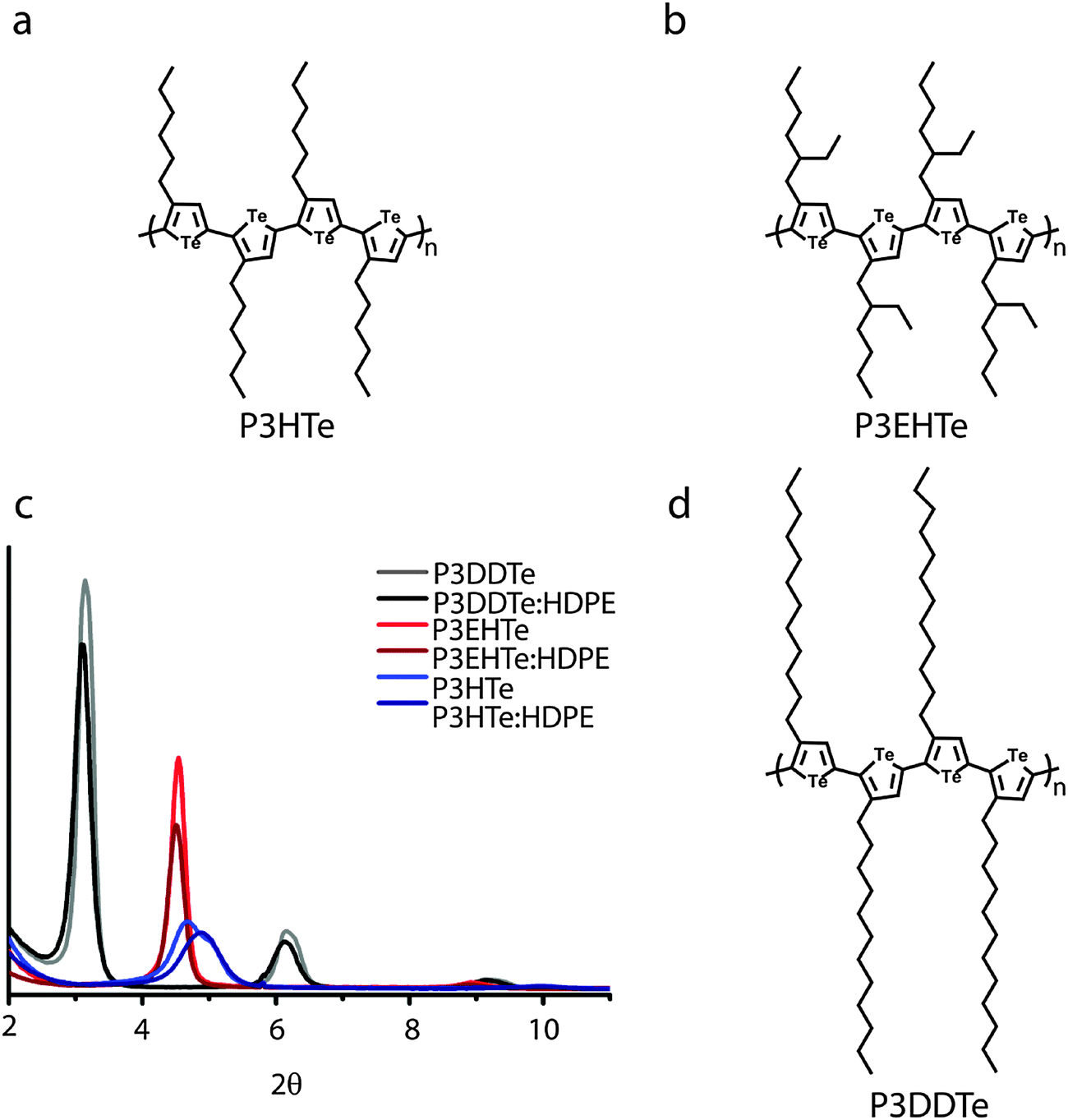 | ||
| Fig. 1 Structures of P3HTe (a), P3EHTe (b) and P3DDTe (d). Grazing-Incidence Wide-Angle X-ray Scattering (GIWAXS) diffractograms of polytellurophene derivatives and their blends with high-density polyethylene HDPE (c). Grey: P3DDTe; black: P3DDTe:HDPE; red: P3EHTe; maroon: P3EHTe:HDPE; blue: P3HTe; navy: P3HTe:HDPE. | ||
We next consider the electrical properties of the polymers and blends. The interface between the gate dielectric and the first several monolayers of active material is an important concern for thin-film transistor measurements. Thus we began by examining various surface treatments on the SiO2 dielectric. Untreated SiO2 surfaces as well as those modified with octadecyltrichlorosilane (OTS) or trichloro(phenyl)silane (TPS) self-assembled monolayers (SAMs) were evaluated. Due to solvent incompatibility we were not able to obtain consistent thin film deposition on OTS coated or unmodified substrates, and device statistics (vide infra) were unattainable. The TPS SAM was chosen for this study because homogeneous thin film deposition was achieved using this modification. The fact that all polymers and blends only work with this one particular modification suggests that their surface requirements (i.e. degree of hydrophobicity and surface energy) are similar.
Field-effect transistor devices were fabricated using the polymers and blends as active layers in the bottom/gate bottom/contact geometry and their electrical performance was evaluated (Fig. 2). P3HTe:HDPE and P3DDTe:HDPE display similar charge-carrier (hole) mobilities (1.6 × 10⁻³ cm2 V−1 s−1 and 5.7 × 10⁻³ cm2 V−1 s−1, respectively) as well as similar on/off ratios (3.4 × 10³ and 4.7 × 10³, respectively) that are fairly average for these types of conjugated polymers, if not good considering their modest molecular weight. On the other hand, P3EHTe:HDPE has a much lower charge-carrier mobility (2.8 × 10⁻⁴ cm2 V−1 s−1) and on/off ratio (2.4 × 10²). To fully appreciate blend electrical performance, the performance of the neat materials must be taken into account. Neat P3EHTe performs quite poorly (mobility of 7.8 × 10⁻⁵ cm2 V−1 s−1 and on/off ratio of 1.0 × 10²), whereas neat P3HTe and P3DDTe both have moderate to good charge-carrier mobilities (1.6 × 10⁻³ cm2 V−1 s−1 for both) and on/off ratios (4.9 × 10³ and 1.1 × 10³, respectively). The relatively poor performance of P3EHTe is very similar to the thiophene analog previously reported29 and is likely due to the branched side chain and not the tellurophene backbone. In the case of P3HTe, the device performance is essentially unchanged from the neat to the blend material. For both P3DDTe and P3EHTe the devices perform 3.6 times better when the blends are employed as the active layer.
 | ||
| Fig. 2 Transfer characteristics of field-effect transistor devices of neat (red) and HDPE blend (blue) active layers for P3HTe (a), P3DDTe (b), and P3EHTe (c). | ||
The different molecular structure packing of the P3ATes has a drastic effect on the solid-state microstructure development of the multicomponent system, as electron microscopy reveals. This insight can be gained because of the enhanced electron scattering obtained through introduction of the tellurium atoms. Let us first consider the P3HTe:HDPE blends: they have striking features at both the nano- and micro-scale (Fig. 3c–f) that differ significantly from either of the two components (Fig. 3a and b). Microscale features consist of randomly packed ∼1 μm diameter spheroids that are surrounded by a matrix. Nanofibers are present within these spheroids as well as in the surrounding matrix (Fig. 3d–f). The nanofibers are rod-like and approximately 50 to 100 nm in length. These types of features are suggestive of the crystalline moieties reported for P3HT,30 yet interestingly these crystallites are not very apparent in neat P3HTe films. Longer fibers, up to 1 μm long, are also distinguishable within the surrounding matrix of the blends. These fibers appear brighter than the matrix (Fig. 3d) under dark-field scanning transmission electron microscopy (STEM), which is indicative of their semi-crystalline nature. Moreover, the elemental contrast provided by backscattered electron imaging suggests that both the spheroids and the surrounding matrix contain tellurium (Fig. S4, ESI†); however, the spheroids have the highest contrast and thus likely are of higher P3HTe content. Energy-dispersive X-ray (EDX) mapping confirms that the fibers contain tellurium (Fig. S5, ESI†).
 | ||
| Fig. 3 Characterization of P3HTe:HDPE blend. Conventional TEM of neat P3HTe thin-film (a). Dark-field STEM image of neat HDPE thin-film (b). Conventional TEM (c, f), dark-field STEM (d), and AFM phase (e) images showing the structure of the P3HTe:HDPE blend thin-film. | ||
In the next example, the P3DDTe:HDPE blends, where a longer alkyl side-chain is used as the solubilizing fragment on the organometallic polymer, it becomes immediately apparent that these structures are very different than P3HTe:HDPE systems in several ways. P3DDTe:HDPE blends consist of high-contrast, irregularly shaped domains that range from 100 nm to several microns in size (Fig. 4b, dark features; Fig. 4c, light features) and are embedded in a matrix (Fig. 4b, light features; Fig. 4c, dark features). The high contrast of these irregularly shaped regions that are observed in both TEM and backscattered electron imaging (Fig. 4f, light features) indicates that they contain the majority of the P3DDTe. EDX mapping confirms that tellurium is solely present in these areas (Fig. 4d and e) and is absent in the surrounding matrix, which is most likely composed predominantly of HDPE. Further support for this assignment comes from the similarity between the structural features we observe in the matrix and that obtained for neat HDPE films (Fig. 3b). Interestingly, none of the nanofibers that are observed in neat P3DDTe (Fig. 4a) are observed within the tellurium-containing domains of the P3DDTe:HDPE blends. Thus we hypothesized that an appreciable amount of HDPE infiltrates this domain and disrupts the P3DDTe nanofiber formation.
 | ||
| Fig. 4 Characterization of P3DDTe:HDPE blend. Conventional TEM of neat P3DDTe thin-film (a). Conventional TEM (b), dark-field STEM (c), and backscattered electron (f) images showing phase separation in the P3DDTe:HDPE composite thin-film morphology. Reference (d) and EDX (e) images showing tellurium (white dots) containing phase. | ||
In the final example, i.e. P3EHTe:HDPE, comprising the branched alky chains that stand in contrast to the highly linear HDPE polymer, another unique blend microstructure is observed. Large, phase-separated domains on the order of several microns are observed (Fig. 5b and c). The dominant phase (Fig. 5c, yellow; Fig. 5d, light features) contains a network (Fig. 5d, blue arrow) that appears to be very similar in structure to films of neat P3EHTe (Fig. 5a) while the smaller regions contain feather-like fibers (Fig. 5d, red arrow) 0.5 to 1 μm in length that are consistent with what is observed in control experiments on neat HDPE films (Fig. 3b). Backscattered electron images (Fig. 5e, light features) and EDX mapping (Fig. 5g–i) confirm that the more abundant phase is the only one that contains tellurium. Interestingly, this is not what we expect because this domain has low contrast in the conventional TEM images. This suggests that the P3EHTe phase is much thinner than the HDPE phase. The AFM height image shows that the P3EHTe domains are indeed of a significantly reduced thickness (∼100 nm) compared to the rest of the film (Fig. 5f, red features). From our observation it is thus clear that the branched side chain derivative is less compatible with HDPE and gives the largest degree of phase separation and contrast between the two materials – findings that likely apply to other semiconductor:insulator blend systems.
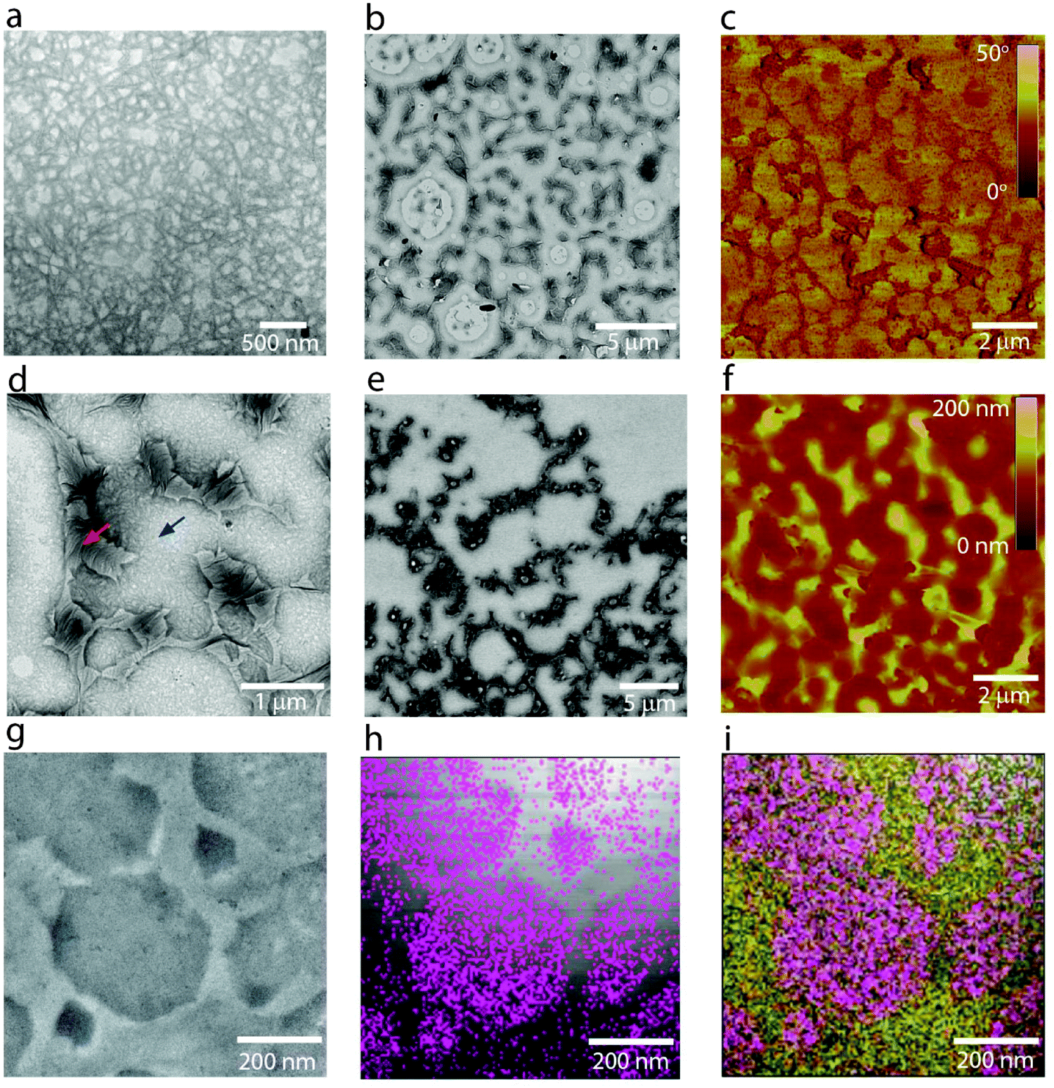 | ||
| Fig. 5 Characterization of P3EHTe:HDPE blend. Conventional TEM image of neat P3EHTe thin-film (a). AFM phase (c) and height (f) images of blend thin-films. Conventional TEM (b, d) and backscattered electron (e) images showing phase separated morphology of P3EHTe:HDPE blend. Reference (g) and EDX (h, i) images showing tellurium (purple) and carbon (yellow) containing phases. | ||
With this imaging data in hand, we can discuss how the molecular structure of the polytellurophene component relates to the blend structure. We can also begin to describe how the blend structure relates to electrical performance, although some consideration must be given to the different substrate used for transistor device testing and its potential effect on film morphology. In the case of P3HTe:HDPE, the P3HTe forms nanofibers (or whiskers31) leading to phase separation from HDPE and causing spheroid formation. The spheroids contain HDPE with imbedded P3HTe nanofibers; P3HTe nanofibers are also within the less ordered surrounding matrix guaranteeing efficient percolation. Of the three systems, this is the only one where there is not a change in the transistor performance going from neat material to blend. It is possible that the blend results in an enrichment of P3HTe on the dielectric surface, similar to what is observed in P3HT:HDPE blends,25 however, characterization of this buried interface is challenging. In P3EHTe:HDPE systems, the two very distinct phases that are observed indicate poor miscibility of the two polymers. In spite of the large phase separated features, the composite outperforms the neat material in transistor devices, indicating that the blend provides for an improved charge transport pathway. Finally, in the case of P3DDTe:HDPE there appears to be a small degree of miscibility between the two polymers causing disruption of nanofibular packing of the P3DDTe phase. Interestingly, this system improved most relative to the neat material that features clearly defined nanofibular features of similar to low-molecular weight P3HT. The degree of solubility of the P3ATes in the solvents used for film casting as well as the crystallization rates of each polymer must also be considered, as they could greatly influence the morphology observed. An interesting future study would be an investigation of the effects of various annealing conditions on the blend morphologies.
Conclusions
In conclusion, we have prepared blends of organometallic polytellurophenes and HDPE and shown that they have unique solid-state microstructures and phase morphologies that are dictated by the alkyl side-chain of the polytellurophene component. The strong contrast provided by the tellurium heavy atom greatly improves phase identification making these systems ideal for studying structure–property–function relationships in semiconductor:insulator blends. The structural similarities to P3HT makes the employment of polytellurophenes particularly useful for enlightening the microstructure of semicrystalline insulating:semiconducting polymer blends. The fact that we observe such different morphologies in all three polymer blend systems and yet measure very similar transport properties is one of the really novel aspects of the work. Elemental contrast appears to be a general strategy for examining the microstructure of polymer blends. This likely can be applied to other systems, for example donor–acceptor type polymers including Si or Ge in place of carbon, P in place of N, or Se or Te in place of S. While these elementally distinct molecules may require greater synthetic effort they nonetheless offer imaging contrast that cannot be achieved with their lighter congeners.Experimental section
Materials
HDPE was purchased from Sigma Aldrich (product number 181900, batch number 04306CH) with a weight average molecular weight Mw of ∼125 kDa, density = 0.95 g mL−1, and Tm = 130 °C. P3HTe, P3DDTe, and P3EHTe were prepared according to published protocols. Briefly, a solution containing isopropylmagnesium chloride lithium chloride complex was used to activate 2,5-diiodo-3-hexyltellurophene in dry methyl THF under a nitrogen atmosphere. The mixture was added to a flask containing [1,3-bis(diphenylphosphino)propane]nickel(II) chloride and the solution was heated to 80 °C for 24–48 hours then quenched with hydrochloric acid and precipitated into methanol. The polymers were purified by soxhlet extraction. Polymer molecular weight was determined by GPC in 1,2,4-trichlorobenzene operating at 140 °C. P3HTe: Mn = 9.9 kDa, Mw = 21.8 kDa, Đ = 2.2. P3DDTe: Mn = 11.3 kDa, Mw = 22.9 kDa, Đ = 2.0. P3EHTe: Mn = 9.0 kDa, Mw = 13.8 kDa, Đ = 1.5. Polymer regioregularity (93%) was obtained by 1H NMR for P3EHTe but was not obtained for P3DDTe and P3HTe due to limited solubility in NMR studies.Thin film preparation
Solutions of 60![[thin space (1/6-em)]](https://www.rsc.org/images/entities/char_2009.gif) :40 P3ATe:HDPE were prepared in 1,2,4-trichlorobenzene at 140 °C using a total polymer content of 5 mg mL−1. Neat films were prepared from solutions in 1,2,4-trichlorobenzene also at a polymer content of 5 mg mL−1. Films were wire-bar coated onto substrates kept at 140 °C and left at 140 °C for 1 additional minute after solvent evaporation. The resulting thin films were then cooled to room temperature and stored in an inert atmosphere. For TEM imaging glass substrates were first wire-bar coated with sodium polystyrene sulfonate from a 15 mg mL−1 solution in a 1:1 (v/v) water:ethanol mixture at room temperature, prior to deposition of neat or blend films as described above. The films were then delaminated using water and transferred onto carbon film coated 300 mesh copper TEM grids purchased from Electron Microscopy Sciences.
:40 P3ATe:HDPE were prepared in 1,2,4-trichlorobenzene at 140 °C using a total polymer content of 5 mg mL−1. Neat films were prepared from solutions in 1,2,4-trichlorobenzene also at a polymer content of 5 mg mL−1. Films were wire-bar coated onto substrates kept at 140 °C and left at 140 °C for 1 additional minute after solvent evaporation. The resulting thin films were then cooled to room temperature and stored in an inert atmosphere. For TEM imaging glass substrates were first wire-bar coated with sodium polystyrene sulfonate from a 15 mg mL−1 solution in a 1:1 (v/v) water:ethanol mixture at room temperature, prior to deposition of neat or blend films as described above. The films were then delaminated using water and transferred onto carbon film coated 300 mesh copper TEM grids purchased from Electron Microscopy Sciences.
Grazing incidence wide-angle X-ray scattering
Grazing incidence wide-angle X-ray scattering measurements were performed at the Cornell High Energy Synchrotron Source (CHESS) D1 beamline. In these experiments, the specimens were exposed at a shallow angle of 0.17° to an incident synchrotron radiation of a wavelength of 1.154 Å. The scattered X-ray was collected with a MedOptics CCD detector with a pixel size of 47 mm and 1024 × 1024 pixels located 103.6 mm away from the specimen. All samples were prepared as described above on Si/SiO2 substrates and measured at room temperature in air.Atomic force microscopy
Images were obtained with a Veeco Dimension 3000 microscope on thin films prepared as described above.Electron microscopy
TEM images were obtained on a Hitachi H-7000 microscope at an accelerating voltage of 100 kV. STEM and backscattered electron images were obtained on a FEI Quanta FEG 250 ESEM at 30 kV. EDX for P3EHTe was obtained with a Thermo Noran System 6 EDX on a JEOL JEM-2010 200 kV high resolution TEM instrument. EDX for P3HTe and P3DDTe were obtained with an Oxford Inca EDX on a Hitachi S-5200 HRSEM at 30 kV.Field-effect transistors
Transistors were fabricated on pre-patterned Si(n++)/SiO2(230 ± 10 nm)/ITO (10 nm)/Au (30 nm) bottom/gate bottom/contact substrates purchased from the Fraunhofer Institute for Photonic Microsystems. The channel length and width of the device geometries used were 5 mm and 10 mm, respectively. Prior to the deposition of the active layers, a trichlorophenylsilane self-assembled monolayer was formed on the SiO2 surface. Polymers and their corresponding blends were then deposited in air following the method described above. All measurements were carried out with in an N2 environment using an Agilent 4155C Semiconductor Parameter Analyzer.Author contributions
D.S.S., N.S., and A.A. designed the research. A.A.J., L.Y., N.C., A.S., and P.M.D. carried out the experiments. A.J.T. contributed to evaluation of transistor device performance and statistics. The manuscript was written through contributions of all authors. All authors have given approval to the final version of the manuscript.Acknowledgements
D. S. S. is grateful to NSERC, the CFI, The Ontario Research Fund, DuPont and DuPont Canada, and the Alfred P. Sloan Foundation. N. S. is in addition supported by a European Research Council (ERC) Starting Independent Research Fellowship (grant agreement no. 279587). This work was also supported by a KAUST Global Collaborative Research Academic Excellence Alliance (AEA) and Competitive Research grant under the grant agreement no. CRG-1-2012-THO-015. The authors would like to thank Cornell High Energy Synchrotron Source (CHESS) for granting us use of the facility. We are also very grateful for the assistance provided by Detlef-M. Smilgies and Ruipeng Li at CHESS. A.A.J. is grateful for the Colin Hahnemann Bayley Fellowship in Chemistry and the University of Toronto Department of Chemistry Special Opportunity Travel Fellowship. P.M.D. is grateful for the F. E. Beamish Graduate Scholarship in Science and Technology and the Jim Guillet Chemistry Graduate Scholarship. A. J. T. would like to thank the Connaught Global Challenge Award for a postdoctoral fellowship.References
- D. R. Paul and L. M. Robeson, Polymer, 2008, 49, 3187–3204 CrossRef CAS PubMed.
- P. M. Ajayan, O. Stephan, C. Colliex and D. Trauth, Science, 1994, 265, 1212–1214 CAS.
- A. Santamaria, M. E. Muñoz, M. Fernández and M. Landa, J. Appl. Polym. Sci., 2013, 129, 1643–1652 CrossRef CAS.
- J. N. Coleman, U. Khan and Y. K. Gun'ko, Adv. Mater., 2006, 18, 689–706 CrossRef CAS.
- M. H. Al-Saleh and U. Sundararaj, Carbon, 2009, 47, 2–22 CrossRef CAS PubMed.
- J. Du and H. Cheng, Macromol. Chem. Phys., 2012, 213, 1060–1077 CrossRef CAS.
- A. C. Balazs, T. Emrick and T. P. Russell, Science, 2006, 314, 1107–1110 CrossRef CAS PubMed.
- K.-J. Jeon, H. R. Moon, A. M. Ruminski, B. Jiang, C. Kisielowski, R. Bardhan and J. J. Urban, Nat. Mater., 2011, 10, 286–290 CrossRef CAS PubMed.
- Y. Kojima and A. Usuki, J. Polym. Sci., Part A: Polym. Chem., 1993, 31, 983–986 CrossRef CAS.
- S. Sinha Ray, K. Yamada, M. Okamoto, A. Ogami and K. Ueda, Chem. Mater., 2003, 15, 1456–1465 CrossRef.
- R. Barrer, J. Barrie and M. Rogers, J. Polym. Sci., Part A: Gen. Pap., 1963, 1, 2565–2586 CrossRef.
- T. Kashiwagi, F. Du, J. F. Douglas, K. I. Winey, R. H. Harris and J. R. Shields, Nat. Mater., 2005, 4, 928–933 CrossRef CAS PubMed.
- A. Dasari, Z.-Z. Yu, G.-P. Cai and Y.-W. Mai, Prog. Polym. Sci., 2013, 38, 1357–1387 CrossRef CAS PubMed.
- M. Si, T. Araki, H. Ade and A. Kilcoyne, Macromolecules, 2006, 39, 4793–4801 CrossRef CAS.
- L. T. Vo and E. P. Giannelis, Macromolecules, 2007, 40, 8271–8276 CrossRef CAS.
- J. Zhou and G. Lubineau, ACS Appl. Mater. Interfaces, 2013, 5, 6189–6200 CAS.
- N. Grossiord, J. Loos, L. van Laake, M. Maugey, C. Zakri, C. E. Koning and a. J. Hart, Adv. Funct. Mater., 2008, 18, 3226–3234 CrossRef CAS.
- J.-C. Lin, W.-Y. Lee, H.-C. Wu, C.-C. Chou, Y.-C. Chiu, Y.-S. Sun and W.-C. Chen, J. Mater. Chem., 2012, 22, 14682 RSC.
- A. Babel and S. A. Jenekhe, Macromolecules, 2004, 37, 9835–9840 CrossRef CAS.
- F. S. Kim and S. A. Jenekhe, Macromolecules, 2012, 45, 7514–7519 CrossRef CAS.
- E. B. Pentzer, F. A. Bokel, R. C. Hayward and T. Emrick, Adv. Mater., 2012, 24, 2254–2258 CrossRef CAS PubMed.
- L. Zhao, X. Pang, R. Adhikary, J. W. Petrich, M. Jeffries-El and Z. Lin, Adv. Mater., 2011, 23, 2844–2849 CrossRef CAS PubMed.
- S. Cho, J. Kwag, S. Jeong, Y. Baek and S. Kim, Chem. Mater., 2013, 25, 1071–1077 CrossRef CAS.
- S. Ren, L.-Y. Chang, S.-K. Lim, J. Zhao, M. Smith, N. Zhao, V. Bulović, M. Bawendi and S. Gradecak, Nano Lett., 2011, 11, 3998–4002 CrossRef CAS PubMed.
- S. Goffri, C. Müller, N. Stingelin-Stutzmann, D. W. Breiby, C. P. Radano, J. W. Andreasen, R. Thompson, R. A. J. Janssen, M. M. Nielsen, P. Smith and H. Sirringhaus, Nat. Mater., 2006, 5, 950–956 CrossRef CAS PubMed.
- A. Kumar, M. A. Baklar, K. Scott, T. Kreouzis and N. Stingelin-Stutzmann, Adv. Mater., 2009, 21, 4447–4451 CrossRef CAS.
- C. E. Murphy, L. Yang, S. Ray, L. Yu, S. Knox and N. Stingelin, J. Appl. Phys., 2011, 110, 093523 CrossRef PubMed.
- A. A. Jahnke, B. Djukic, T. M. McCormick, E. Buchaca Domingo, C. Hellmann, Y. Lee and D. S. Seferos, J. Am. Chem. Soc., 2013, 135, 951–954 CrossRef CAS PubMed.
- D. T. Duong, V. Ho, Z. Shang, S. Mollinger, S. C. B. Mannsfeld, J. Dacuña, M. F. Toney, R. Segalman and A. Salleo, Adv. Funct. Mater., 2014, 24, 4515–4521 CrossRef CAS.
- R. J. Kline, M. D. McGehee, E. N. Kadnikova, J. Liu, J. M. J. Fréchet and M. F. Toney, Macromolecules, 2005, 38, 3312–3319 CrossRef CAS.
- K. J. Ihn, J. Moulton and P. Smith, J. Polym. Sci., Part B: Polym. Phys., 1993, 31, 735–742 CrossRef CAS.
Footnote |
| † Electronic supplementary information (ESI) available: Further detail for GIWAXS data, supporting electron microscopy images, and transistor device output characteristics. See DOI: 10.1039/c5tc00158g |
| This journal is © The Royal Society of Chemistry 2015 |