
 Open Access Article
 This Open Access Article is licensed under a
 Creative Commons Attribution 3.0 Unported Licence
Vertical stratification and its impact on device performance in a polycarbazole based copolymer solar cells†
Tao
Wang
*ab,
Nicholas W.
Scarratt
a,
Hunan
Yi
c,
Iain F.
Coleman
c,
Yiwei
Zhang
a,
Richard T.
Grant
a,
Jizhong
Yao
d,
Maximilian W. A.
Skoda
e,
Alan D. F.
Dunbar
f,
Richard A. L.
Jones
a,
Ahmed
Iraqi
*c and
David G.
Lidzey
*a
aDepartment of Physics and Astronomy, University of Sheffield, Sheffield S3 7RH, UK. E-mail: d.g.lidzey@sheffield.ac.uk
bSchool of Materials Science & Engineering, Wuhan University of Technology, Wuhan 430070, China. E-mail: twang@whut.edu.cn
cDepartment of Chemistry, University of Sheffield, Sheffield S3 7HF, UK. E-mail: a.iraqi@sheffield.ac.uk
dCentre for Plastic Electronics and Department of Physics, Blackett Laboratory, Imperial College London, London SW7 2AZ, UK
eISIS Pulsed Neutron and Muon Source, Science and Technology Facilities Council, Rutherford Appleton Laboratory, Harwell Science and Innovation Campus, Didcot OX11 0QX, UK
fDepartment of Chemical and Biological Engineering, University of Sheffield, Sheffield S1 3JD, UK
First published on 11th March 2015
Abstract
Using neutron-reflectivity, we study vertical stratification and device performance in bulk hetero-junction organic photovoltaic (OPV) cells consisting of a blend of PC71BM with a carbazole-based donor–acceptor copolymer PCDTBT1. We find that when the blend is cast on a PEDOT:PSS/ITO anode, a PC71BM-depleted (polymer-rich) layer is formed at the PEDOT:PSS interface, whilst a PC71BM-depleted layer is instead located at the air-interface when the same blend is cast on a solution processed MoOx thin film. OPV device characterization measurements indicate that unfavourable vertical segregation can have a profound effect on OPV device characteristics via increased charge recombination.
1. Introduction
Bulk heterojunction (BHJ) organic photovoltaic (OPV) devices employing conjugated polymers as electron donors and fullerene derivatives PCBM as electron acceptors convert the energy of sunlight directly into electric current based on the photovoltaic effect.1,2 This type of device represents a promising renewable energy source and has attracted significant attention due to the potential of solution-processability over large-area on mechanically-flexible substrates using low cost manufacturing techniques. BHJ OPV devices using donor–acceptor (D–A) copolymers as electron donors and PC71BM as electron acceptor have now been used to create organic photovoltaic (OPV) devices having a power conversion efficiency (PCE) over 10% in single junction solar cells3 and 10.6% in tandem solar cells.4To fabricate an OPV device, a bulk heterojunction layer is usually deposited from a solution containing both electron donor (e.g. a conjugated polymer) and an electron acceptor (e.g. the fullerene derivative PCBM). After the evaporation of the solvent, a thin film of tens to hundreds of nanometers thick is created that acts as the solar cell active layer. A complex evolution of film morphology can occur during this solution casting and film drying process that includes phase separation and vertical stratification.5,6 A significant body of work has shown that the nanoscale morphology in both lateral and vertical directions within a BHJ film plays a critical role in determining the efficiency of an organic photovoltaic device.7 For example, lateral morphology (e.g. domain size, purity and connectivity within the BHJ layer) has been widely investigated using both morphological8 and scattering techniques.9–11 Techniques such as neutron reflectivity (NR),12 dynamic secondary ion mass spectroscopy (DSIMS),13 X-ray reflectivity (XRR),14 X-ray photoelectron spectroscopy (XPS),15–17 near edge X-ray absorption fine structure spectroscopy (NEXAFS)18,19 and spectroscopic ellipsometry (SE)20 have been used to examine the vertical distribution of the components within polymer–fullerene thin film blends.
The technique of specular neutron reflectivity (NR) has proved to be particularly successful in determining vertical composition in BHJ bends; although this technique requires a longer measurement time due to the low neutron flux intensity, it benefits from a significant scattering length density (SLD) contrast between conjugated polymers (∼1.0 × 10⁻⁶ Å−2) and fullerenes (>4.0 × 10⁻⁶ Å−2) and has been used to study the vertical component distribution in P3HT:PCBM12,21–23 and low band-gap polymer:PCBM24–26 photovoltaic blends. Furthermore, NR can also measure samples covered by a metallic cathode layer and thus provides an opportunity to probe the effects of surface on modification of the depth profile formed during thermal annealing.27 In this work, we report a study of the structure of a BHJ film made of PC71BM and a carbazole-based D–A copolymer termed PCDTBT1, and show that the vertical stratification in the film driven by the nature of the underlying substrate plays a significant role in determining the eventual device characteristics and efficiency of the OPV device.
2. Experimental
The structure of polymer PCDTBT1 (molecular weight and polydispersity of 57.3 kDa and 2.02 respectively) is shown in Fig. 1(a), with its preparation described in the ESI† to this paper. PCDTBT1 and PC71BM were dissolved in chlorobenzene at a concentration of 10 and 40 mg ml−1 respectively, and put on a hot plate held at 70 °C for 1 h. The solutions were then allowed to cool to room temperature and blended at a number of different blend-ratios. To cast thin films, we have used both spin- and spray-coating. Spray coating was performed using a Prism ultrasonic spray-coating system (Ultrasonic Systems, Inc.), with deposition parameters described in our previous work.25 Thin-films were cast on two different hole transport layers; PEDOT:PSS and a solution-processed MoOx film (henceforth termed sMoOx). The PEDOT:PSS (HC Starck Clevios P AI4083) was spin cast from a water-based solution in air, forming a film having a thickness of around 30 nm. This film was then annealed at 110 °C for several minutes to evaporate any absorbed moisture before the deposition of the active layer. sMoOx films were deposited from an ammonium molybdate tetrahydrate precursor that was dissolved in a blend of water and acetonitrile at a solid content around 3.5 mg ml−1 and then spin cast at 3000 rpm for 30 seconds. This precursor-film was then thermally annealed at 350 °C for 1 min under ambient conditions to create a 10 nm thick sMoOx film having a typical surface roughness ca. 1 nm and a workfunction of ca. 5.17 eV as previously measured by ultraviolet photoelectron spectroscopy.28 The thickness of all thin films was measured using a spectroscopic ellipsometer (M2000v, J.A. Woollam Co., USA). | ||
| Fig. 1 (a) The chemical structure of PCDTBT1. (b) Absorption spectra of PCDTBT1 in solution and when cast into a thin film. (c) Cyclic voltammetry curves recorded on a PCDTBT1 thin film. (d) and (e) A energy-level diagram of the OPV devices studied using two different hole transport layers (PEDOT:PSS and sMoOx). | ||
The samples for neutron reflectivity measurement were either spin or spray cast on a PEDOT:PSS or sMoOx surface. The PEDOT:PSS or sMoOx films were fabricated by spin-casting on a silicon wafer having a 5 nm SiOx surface-layer. Neutron reflectivity measurements were performed on the INTER reflectometer at the ISIS pulsed neutron source at the Rutherford Appleton Laboratory, UK. Reflectivity data were recorded over the wavelength range 1.5 Å to 15 Å at two different angles (0.5° and 2.3°). The data-sets were then combined to give a q range from 0.01 Å−1 to 0.2 Å−1, with a resolution of Δq/q = 0.03. Beyond this q-range, we find that the reflectivity was dominated by the scattering background. The NR data was analyzed using a slab model consisting of multiple, thin stacked layers, with each layer being assigned a thickness, roughness and a scattering length density (SLD).12 The data was fitted using RASCAL software developed at ISIS.
Dynamic (water) contact angles were measured using a Theta Optical Tensiometer. Here, a droplet of water (having a volume of around 8 μL) was deposited onto a film surface of interest with a sequence of images recorded every second over a period of 60 seconds. The contact angle was then determined from each image using the average of the contact angles determined from either side of the droplet. For each film, three independent measurements were performed at different locations on the film surface.
OPV devices were defined on pre-patterned ITO substrates purchased from Ossila Ltd. The ITO/glass substrates were first cleaned by sonication in dilute NaOH followed by IPA. The ITO/glass substrate used in this work had an area of 20 × 15 mm2, onto which six pixels were defined, each having an area of 4.5 mm2. All active layers were either spin or spray-coated in air onto the glass/ITO/anode substrate, following which they were transferred to a nitrogen glovebox connected to a thermal evaporator system for deposition of the OPV cathode (5 nm of calcium capped by a 100 nm of aluminum evaporated at a base pressure of ∼10−7 mbar). The cathode was deposited through a shadow-mask, producing a series of independent pixels. Devices were finally encapsulated using a glass slide and epoxy glue before testing. PCEs were determined using a Newport 92251A-1000 AM1.5 solar simulator. An NREL calibrated silicon cell was used to calibrate the power output to 100 mW cm−2 at 25 °C. At least two devices were prepared for each sample and device parameters from 12 pixels were collected to report the average values presented in Table 2. A recent cross-check of the accuracy of our solar simulator system and calibrated silicon solar cell with a solar simulator at Loughborough University UK (CREST) indicated that the systematic uncertainty on the device PCE quoted here (Δη/η) is around 5%. The structures of the hole-dominated and electron-dominated devices are glass/ITO/PEDOT:PSS/active layer/Au and glass/ITO/Al/active layer/Ca/Al, respectively.
3. Results and discussion
The conjugated copolymer PCDTBT1 (see the chemical structure in Fig. 1(a)) consists of a carbazole donor moiety, flanked by two thienyl groups that are co-polymerized with a benzothiadiazole (BT) acceptor. This BT acceptor group is itself functionalized with two alkoxy side-chains to impart improved solubility. Our grazing-incidence X-ray measurements suggest that PCDTBT1 is a largely amorphous polymer when deposited from solution, with weak order in the form of π–π stacking. The optical absorption spectrum of PCDTBT1 is shown in Fig. 1(b). It can be seen that in chloroform, PCDTBT1 has an absorption maximum (λmax) at 518 nm, with λmax being red-shifted to 535 nm on casting into a solid film. From the absorption spectrum (onset of absorption band), we determine an optical-bandgap for PCDTBT1 as 1.90 eV. Cyclic voltammetry measurements performed on PCDTBT1 are shown in Fig. 1(c), from which HOMO and LUMO levels of −5.4 and −3.2 eV are determined. The energy level diagrams of OPV devices in this work are depicted in Fig. 1(d) and (e).From device studies, we determined that the optimum device efficiency occurs at a PCDTBT1![[thin space (1/6-em)]](https://www.rsc.org/images/entities/char_2009.gif) :PC71BM blend ratio of 1:4. At this point, device efficiency is 10% higher than in devices based on a PCDTBT1 and PC71BM blend ratio of 1:3, and much higher than devices with blending ratios of 1:2 and 1:1 (see Fig. S1a, ESI†). This optimum blend ratio is in fact similar to that determined in photovoltaic blends of PC71BM with other carbazole-based D–A copolymers (e.g. PCDTBT and PCDTBT829). Thermal annealing of the devices was found to be detrimental to device efficiency, an effect similar to OPV devices made of many donor–acceptor copolymers.30,31 The structure and device studies in this work were therefore performed with the photovoltaic films in an as-cast state without any thermal annealing treatment.
:PC71BM blend ratio of 1:4. At this point, device efficiency is 10% higher than in devices based on a PCDTBT1 and PC71BM blend ratio of 1:3, and much higher than devices with blending ratios of 1:2 and 1:1 (see Fig. S1a, ESI†). This optimum blend ratio is in fact similar to that determined in photovoltaic blends of PC71BM with other carbazole-based D–A copolymers (e.g. PCDTBT and PCDTBT829). Thermal annealing of the devices was found to be detrimental to device efficiency, an effect similar to OPV devices made of many donor–acceptor copolymers.30,31 The structure and device studies in this work were therefore performed with the photovoltaic films in an as-cast state without any thermal annealing treatment.
Fig. 2(a) shows neutron reflectivity curves of the three blend films deposited by spin or spray-coating on the surface of two different hole transport layers (HTL); PEDOT:PSS and sMoOx. Here, the solid symbols correspond to the measured reflectivity data points, whilst the magenta lines are a fit using a slab model consisting of multiple thin layers, as described in our previous work.12,25 As input to the model, values of scattering length density (SLD) of PCDTBT1 and PEDOT:PSS were calculated from the NIST online database32 and had values of 1.40 × 10⁻⁶ and 1.80 × 10⁻⁶ Å−2 respectively. A value of 4.74 × 10⁻⁶ Å−2 was used as the SLD of PC71BM, as has been reported in the literature.33 The parameters from the best fit are summarized in Table 1.
 | ||
| Fig. 2 (a) Neutron reflectivity of PCDTBT1:PC71BM (1:4) blends spin and spray cast on PEDOT:PSS, as well as spray cast on sMoOx surface. The curves are vertically shifted for clarity. Part (b) shows a SLD profile of PCDTBT1:PC71BM (1:4) blend deposited by spin-casting on a PEDOT:PSS surface, with parts (c) and (d) showing the SLD of the same film spray-cast on a PEDOT:PSS and sMoOx surface respectively. | ||
:PC71BM 1:4 blend film deposited on different HTLs by spin or spray coating
| Spin cast on PEDOT:PSS | Spray cast on PEDOT:PSS | Spray cast on sMoOx | |
|---|---|---|---|
| Thickness of the bulk layer (nm) | 60 ± 2 | 60 ± 2 | 59 ± 2 |
| SLD of the bulk layer (×10−6 Å−2) | 4.10 ± 0.16 | 4.04 ± 0.18 | 4.06 ± 0.20 |
| PC71BM content in the bulk layer (wt%) | ∼86 ± 3 | ∼84.5 ± 4 | ∼85 ± 5 |
| Thickness of the depleted region (nm) | 5.2 ± 0.4 | 10 ± 0.6 | 9.8 ± 0.6 |
| SLD of the depletion region (×10−6 Å−2) | 1.42 ± 0.1 | 1.42 ± 0.1 | 1.42 ± 0.1 |
| PC71BM content in the depletion region (wt%) | ∼1 ± 0.2 | ∼1 ± 0.2 | ∼1 ± 0.2 |
| Roughness at air interface (nm) | 0.5 ± 0.1 | 0.5 ± 0.1 | 2 ± 0.2 |
| Roughness of depleted-bulk interface (nm) | 1.2 ± 0.1 | 3 ± 0.2 | 7 ± 0.4 |
| Roughness at HTL interface (nm) | 2 ± 0.2 | 2 ± 0.2 | 2.8 ± 0.2 |
Fig. 2(b) plots the calculated SLD profile of PCDTBT1:PC71BM spin cast on a PEDOT:PSS film surface. We find that the vertical concentration of PC71BM throughout the active layer is not uniform. The PC71BM distribution is initially constant in the region from the surface through the middle of the film, but then undergoes a relative reduction in concentration towards the PEDOT:PSS interface. We define the region across which the PC71BM content is constant as the “bulk layer”, and the region where the PC71BM content is less than 80% (corresponding to a 1:4 blending ratio) as the “PC71BM depleted region”. The weight fraction of the PC71BM component in the blend films was determined following the method described in the literature,33 with the density of PCDTBT1 and PC71BM taken as 1.1 and 1.61 g cm−3 respectively. The PC71BM depleted layer is identified in Fig. 2, together with the location of the Si/SiOx layer, the PEDOT:PSS layer and the bulk polymer:fullerene layer. Our NR fits indicate an SLD value of 4.1 × 10⁻⁶ Å−2 in the bulk layer, corresponding to a PC71BM content of 86%. The PC71BM depleted layer near the PEDOT:PSS interface had an SLD of 1.42 × 10⁻⁶ Å−2, corresponding to a PC71BM concentration of around 1%. This suggests that the interface region near the substrate is comprised of almost pure PCDTBT1 and contains very little PC71BM when cast on PEDOT:PSS. This behavior is in qualitative accord with the vertical stratification observed in other photovoltaic blends made from PC71BM and carbazole-based conjugated polymers.7,25 For example, such a PC71BM depleted layer was also observed near the anode interface in PCDTBT:PC71BM, PCDTBT8:PC71BM and PCDT2BT8:PC71BM 1:4 blends that were cast on a PEDOT:PSS film.7,25 However, in such films, the concentration of PC71BM in the depleted layer was always found to be greater than 60%. Further studies to explore the effects of molecular structure of the conjugated polymer on vertical stratification is currently in progress.
To determine whether the technique used to deposit the PCDTBT1:fullerene blend film played a significant role in directing this vertical segregation, we have deposited a PCDTBT1:PC71BM blend film by spray-casting. Here, the film was spray cast onto a PEDOT:PSS film from a CB solution with the substrate held at a temperature of 40 °C (corresponding to the optimal spray conditions for optimal OPV efficiency as identified in our previous work on this type of copolymer solar cell).25 The SLD profile of this film is shown in Fig. 2(c). Again, we find a PC71BM depleted region is observed near the PEDOT:PSS interface. The SLD of this layer is around 1.42 × 10⁻⁶ Å−2, again indicating that it is composed of almost pure PCDTBT1. Note that in our previous work,25 we found that by spray-casting a polymer:fullerene blend onto a substrate held at a temperature in excess of that used here (40 °C), the film drying kinetics could be accelerated with vertical stratification of the PC71BM during film formation being suppressed. The fact that a similar degree of vertical stratification is observed here by both spin- and spray-casting (see Fig. 2(b) and (c)) indicates that the drying kinetics of a PCDTBT1:PC71BM film formed by spray-casting on a PEDOT:PSS substrate held at 40 °C are very similar to those spin-cast at room temperature.
Fig. 2(d) shows the SLD profile of a PCDTBT1:PC71BM film spray-cast onto a solution-processed molybdenum oxide (sMoOx) film. Here, a very different vertical composition is formed; it can be seen that a PC71BM depleted region having a thickness of 9.8 nm is instead observed at the film-surface; a location that will clearly correspond to the cathode-interface in a regular (non-inverted) OPV device.
To further confirm that the surface-compositions of PCDTBT1:PC71BM films deposited on PEDOT:PSS and sMoOx are different, we have used water contact angle measurements to characterize the surface property of the films. This is shown in Fig. 3, where we plot the contact angle as a function of time after the deposition of the water droplet on a PC71BM, PCDTBT1, PCDTBT1:PC71BM/sMoOx and a PCDTBT1:PC71BM/PEDOT:PSS surface. We find that the contact angle reduces gradually as the system evolves towards an equilibrium state even after 60 seconds. This is most obvious for the water droplets on a PC71BM film, with the contact angle changing from an initial value of 102° to around 93° after 60 seconds. We believe this change in contact angle is indicative of adsorption of water molecules by the PC71BM molecules. Indeed, we believe this water adsorption most likely explains the apparent spread of contact-angle values reported in the literature for PCBM.13,19,34 We also find that when making contact-angle measurements on a PCDTBT1:PC71BM film deposited on PEDOT:PSS film, the contract angles reduce slowly in the first 10–15 seconds and then dramatically level off in to an angle of less than 10° as can be seen in Fig. 3(d). We suspect that water molecules diffuse through the active layer and penetrate the PEDOT:PSS interface causing it to swell. This swelling of PEDOT:PSS increases the porosity of the active layer by opening up pinholes or diffusion channels which further increase the diffusion of water. This results in a delamination of the PEDOT:PSS film from the silicon substrate as manifested by a dramatically reduced contact angle. Thus as the contact angle evolves throughout the course of the experiment, we report the initial contact angle value that is recorded as soon as the water droplet lands on the film surface, rather than selecting an angle at an arbitrary time by assuming that the water droplet has reached the equilibrium state.
 | ||
| Fig. 3 Dynamic water contact angle measurements on films of (a) PC71BM cast on silicon; (b) PCDTBT1 cast on silicon; (c) PCDTBT1:PC71BM 1:4 spray cast on sMoOx; and (d) PCDTBT1:PC71BM 1:4 spray cast on PEDOT:PSS. | ||
Using this approach, we determine contact angles of water on pure PC71BM and PCDTBT1 films of 102° and 96° respectively. For the blend film cast on sMoOx, the water initially assumes a contact angle of around 97°; a value consistent with that of a pure PCDTBT1 film. This suggests that the surface region of this film is mostly composed of pure PCDTBT1. However for the blend film cast on PEDOT:PSS, the water initial assumes a contact angle of around 100°, indicative of a PC71BM-rich phase (refers to the bulk layer of a blend film) near the film surface. Such water contact angle measurements are therefore consistent with our neutron scattering analysis and suggest that the surface composition of a PC71BM:PCDTBT1 blend is highly dependent on the nature of the underlying substrate.
Our measurements thus indicate that vertical composition of a 1:4 blends PCDTBT1:PC71BM is dependent on the nature of the substrate on which it is cast. A review of different reports in the literature7 suggests that vertical stratification in polymer:fullerene bulk heterojunction photovoltaic blends is likely to be materials system dependent, with the driving force being the interplay of thermodynamic stability and kinetic limitations during film drying process. We believe therefore that the non-uniform vertical composition we observe here is driven by selective solubility of polymer and fullerene in the casting solvent that either favours or limits the respective diffusion kinetics of each component during the film drying process. Other work has previously reported vertical segregation in polymer–fullerene blend films, including the closely related polymer PCDTBT in which a PCBM-depleted region was identified around the substrate interface.24,25 We note that in comparison with PCDTBT, the BT unit in PCDTBT1 that has been functionalized with two alkoxy side-chains will impart significantly improved solubility to the polymer.29 We speculate that if the solubility of PCDTBT1 approaches – or even exceeds – that of PC70BM in CB, it is possible that the order in which each material vitrifies during film drying may change,35 with fullerene aggregates forming before the polymer fully vitrifies. Furthermore, the enhanced solubility of PCDTBT1 may well permit it to undergo increased diffusion during film drying. The interactions between the inorganic sMoOx and conjugated PCDTBT1 is not expected to be strong, thus as the PCDTBT1:PC70BM blend solution is cast onto it, the solvated PCDTBT1 chains may preferentially diffuse to the surface region to minimize the total surface energy of the blend film, and create a polymer-rich surface layer. Notably however such solvated PCDTBT1 chains appear to diffuse to the substrate interface when cast on a PEDOT:PSS; a process that will be driven by the thermodynamic interactions between PCDTBT1 and PEDOT:PSS. We note that similar polymer-rich surface layers (having a thickness of around 5 nm) have also been identified in a P3HT:PCBM blend cast on low temperature annealed sMoOx surface.36 In another work investigating PCDTBT:PC70BM blend, an unfavorable polymer-rich layer was also identified near cathode interface upon thermal annealing at a temperature higher than 140 °C.37
To explore the effect of vertical segregation on the operational efficiency of PCDTBT1:PC71BM based OPVs, we have fabricated solar-cell devices utilizing both PEDOT:PSS and sMoOx as hole transport layers. We first fabricated a series of OPV devices to identify the thickness of the active layer at which device efficiency is maximized. This is shown in Fig. 4 where we plot PCE, Voc, FF and Jsc as a function of active layer thickness for OPVs utilizing a PEDOT:PSS anode. It can be seen that an optimized PCE of around 4% was obtained for an active layer thickness of approximately 60 nm. The maximum values of Jsc, Voc and FF are at the thickness ca. 75, 40 and 60 nm, respectively. We note that the maximum Voc values achieved in PCDTBT1:PC71BM solar cell devices (0.98 V) are amongst the highest values reported from carbazole-based donor–acceptor copolymers, e.g. PCDTBT, PCDTBT8.25,29 We believe such high Voc value can be accounted for by the strong vertical segregation in these films, with the high polymer concentration found towards the PEDOT:PSS anode expected to block electron leakage-currents and aid hole extraction.
 | ||
| Fig. 4 Device metrics of spin-cast PCDTBT1:PC71BM (1:4) solar cells using PEDOT:PSS as HTL. | ||
Additional confidence in our device optimization process can be confirmed on the basis of modeling studies. Here, we have extracted the optical constants (n & k, see Fig. S1(b), ESI†) of PCDTBT1:PC71BM 1:4 blend film cast from CB following the methods used in our previous work,38,39 and have simulated the maximum achievable photocurrent as a function of active layer thickness (see Fig. S1(c), ESI†) using a transfer matrix reflectivity model that we have previously employed for PCDTBT:PC71BM devices.40 We find that Jsc first takes its maximal value at a film thickness of ca. 70 nm; a value very close to the optimum thickness determined from our empirical experiments (see Fig. 4(a)).
In Fig. 4(b) it can be seen that both FF and Voc reduce as the PCDTBT1:PC71BM active layer thickness is increased beyond 40 and 60 nm respectively. The observation of reduced FF is consistent with increasingly inefficient charge extraction and concomitant recombination.41 A range of mechanisms have been proposed to account for the Voc loss, including band bending at the device electrodes,42 energetic disorder,43 the existence of charge transfer states,44,45 charge recombination,46 as well as charge selectivity at the active layer/electrode interfaces.47 The carbazole copolymer explored here is a largely amorphous material having relatively low charge-carrier mobility. We have determined the hole and electron mobility from the dark J–V measurements of hole- and electron-dominated devices, and found that μhole = 1.54 × 10⁻⁵ cm2 V−1 s−1, with μelectron = 9.12 × 10⁻⁵ cm2 V−1 s−1. Therefore charge extraction can become problematic when the active layer is too thick. It is likely that in our devices, part of the observed reduction in Voc results from energetic disorder and charge recombination, resulting from the low degree of structure order in these amorphous copolymers.
Using the optimized deposition conditions determined from our previous work,25 we have used spray-casting to fabricate PCDTBT1:PC71BM OPVs onto a PEDOT:PSS/ITO and a sMoOx/ITO anode. We summarize key device metrics in Table 2, along with the devices series and shunt-resistance as extracted from the J–V curve. The devices utilizing the PEDOT:PSS/ITO anode had the highest PCE of 4.1%; a value comparable to that created by spin coating (highest PCE ∼ 4.0%) – see J–V curves for a spin-cast and spray-cast devices in Fig. 5(a) and (b) respectively. In contrast, the PCE of comparable devices either spin- or spray cast onto the sMoOx/ITO anode is significantly reduced, having a value of around 1.4% (again see Fig. 5(a) and (b)). This reduced efficiency is reflected in both reduced average and peak PCE values as can be seen in Table 2. It can be seen that reduction in efficiency of devices fabricated onto sMoOx primarily results from a large drop in Voc going from 0.97 V to 0.57 V, and FF going from 50% to 30%. The average device metrics and their standard deviations from 12 pixel devices for each are also summarized in Table 2.
| Deposition method | HTL | J sc (mA cm−2) | V oc (V) | FF (%) | PCE (%) | R shunt (Ω cm2) | R series (Ω cm2) |
|---|---|---|---|---|---|---|---|
| Spin-cast | PEDOT:PSS |
8.25
(8.40 ± 0.11) |
0.97 (0.95 ± 0.01) | 50.0 (49.1 ± 0.82) | 4.00 (3.93 ± 0.11) | 568 | 12 |
| Spin-cast | sMoOx |
7.84
(7.79 ± 0.30) |
0.58 (0.55 ± 0.05) | 30.9 (31.9 ± 0.80) | 1.41 (1.39 ± 0.28) | 122 | 39 |
| Spray-cast | PEDOT:PSS |
8.80
(8.70 ± 0.11) |
0.96 (0.96 ± 0.01) | 48.5 (48.5 ± 0.82) | 4.10 (4.05 ± 0.07) | 450 | 11 |
| Spray-cast | sMoOx |
8.33
(7.85 ± 0.21) |
0.56 (0.55 ± 0.03) | 31.8 (32.7 ± 0.79) | 1.48 (1.41 ± 0.26) | 121 | 28 |
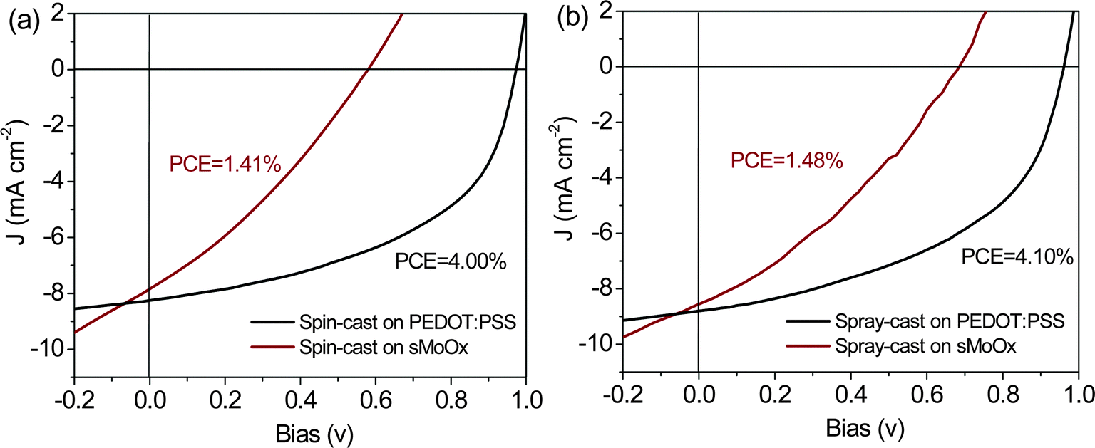 | ||
| Fig. 5 J–V curves of PCDTBT1:PC71BM solar cells using PEDOT:PSS and sMoOx as HTL by (a) spin casting and (b) spray casting in air. | ||
We believe the reduced efficiency of devices utilizing a sMoOx hole extraction layer results from unfavourable vertical stratification within the active layer (i.e. a 10 nm thick polymer-rich layer located at the cathode interface), rather than a failure of the sMoOx layer to act as an effective anode material. Indeed, we have previously created polymer:fullerene blend OPVs using a sMoOx anode, with devices based on the polymer PCDTBT having a peak PCE of 4.4%. Other work has also demonstrated that solution-processed MoO3 films containing a small fraction of oxygen vacancies can act as an efficient hole-extraction layer in organic solar cells.48
It is apparent that the segregated polymer-rich layer at the cathode interface in OPVs based on a sMoOx anode causes a small reduction in Jsc but results in a significant reduction in both Voc and FF. We note previous Monte Carlo charge transport simulations have been used to quantify the effect of surface wetting layer on photocurrent generation within bulk heterojunction PV devices.49 Such simulations demonstrated that minimal reductions in charge extraction efficiency occur providing the composition of the “wrong” component in the wetting layer was less than 85%, with a reduction in photocurrent of around 30% expected even when the fraction of the “wrong” component reaches 95%. Other experimental studies on P3HT:PCBM OPVs have shown that a PCBM fraction as low as 3% in the P3HT wetting layer is sufficient to provide a percolation pathway for electron extraction.50 Here, our neutron-reflectivity fits suggest that the PC71BM fraction in the PCDTBT1 rich layer is less than 1%, with the device Jsc being some 95% of that observed in devices in which there is a large surface concentration of PC71BM. Notably however, the device Voc and FF are substantially reduced as a result of the polymer-rich surface-layer at the cathode interface. We believe this results from bimolecular recombination at the polymer-rich layer interface; a problem that becomes more acute at higher forward drive-bias. This effect is similar to that observed in previous work36,51,52 in which the electron/hole-blocking layer in an OPV device was also found to have a substantial influence on Voc but only have minor impact on Jsc.
The effect of a polymer-rich layer near the cathode interface apparently manifests itself in a reduced shunt resistance (see Table 2). We have further explored the operation of our devices by measuring their light ideality factors under light illumination. Light ideality factors were firstly determined by fitting a straight line to the plots in Fig. S2(a) (ESI†). However, it has been suggested that ideality factor determined by fitting a straight line to the Vocversus light intensity plot will average different recombination mechanisms.53 The light-ideality factor (nid,l) is therefore determined differentially by 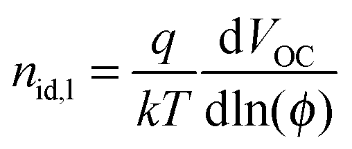 , where q is the electron charge, k is Boltzmann's constant, T is the absolute temperature, and ϕ is the fractional light intensity normalized to one sun.53 The results are plotted in Fig. S2(b) (ESI†). From our linear fits, we found nid,l, of PCDTBT:PC71BM device with PEDOT:PSS as HTL is 1.19. In contrast, nid,l value is 6 when sMoOx is used as HTL. From the differential fit, we found that when operating at one sun, the nid,l, is again around 1.2 for the device with PEDOT:PSS as the HTL, and is much higher than 2 for the device with sMoOx as the HTL. A nid,l, of around 1.2 indicates the presence of both bimolecular and trap-assisted recombination in the device.54 However, the high nid,l value observed (>2) cannot simply be explained by an interplay of different recombination mechanisms. Instead, we attribute such large ideality factors to a small shunt resistance that is caused by unfavorable vertical segregation.
The shunt resistance of a device can often be reduced by the presence of pinholes in the film, as well as recombination and trapping of charge carriers during their transit towards the electrodes.55 We have used interferometric mapping measurements to characterize film morphology (see Fig. 6) and find that PCDTBT1:PC71BM films deposited on a sMoOx anode are uniform and pin-hole free over areas of up to ∼0.30 mm2. This suggests that the reduction in the effective-shunt resistance observed in such devices might be a consequence of bimolecular recombination caused by the polymer-rich layer near the cathode interface. In contrast, PCDTBT1 based devices utilizing a PEDOT:PSS anode do not have such a polymer-rich layer towards the cathode interface, and thus have increased FF, Voc and shunt-resistance and thus improved device efficiency.
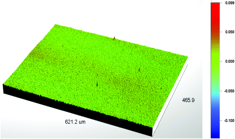 | ||
| Fig. 6 Optical interferometry image of a PCDTBT1:PC71BM (1:4) film cast on sMoOx film surface. | ||
4. Conclusions
We have observed contrasting vertical stratification of the PC71BM component in PCDTBT1:PC71BM photovoltaic blends cast by two different methods on two different hole transport layers. Although the precise mechanism of solution deposition (spin-casting versus spray-casting) did not significantly affect vertical composition within the film, we found that the nature of the hole-transport layer significantly affects the vertical stratification of PCDTBT1:PC71BM blends. Specifically, we found that in a 1:4 PCDTBT1:PC71BM blend, a PC71BM-depleted layer was located at the substrate interface in films cast upon a PEDOT:PSS/ITO anode, whilst this polymer-rich layer was instead located at the air-interface when the same film was cast onto a solution-cast MoOx film. Device studies indicate the importance of such vertical segregation, as a PC71BM-depleted layer located at the cathode interface was shown to reduce the extraction efficiency of charge and thus increase charge recombination, which results in a sharp reduction in open circuit voltage and fill-factor.
Acknowledgements
We thank financial support from EPSRC via grant EP/I028641/1 “Polymer/fullerene photovoltaic devices: new materials and innovative processes for high-volume manufacture” and for funding the Supergen Supersolar Hub (EP/J017361/1). We thank Andrew Pearson (now at University of Cambridge), Darren Watters (University of Sheffield) and Tom Glen (University of Cambridge) for assistance with the neutron scattering beamline experiments at ISIS. We thank Jenny Nelson (Imperial College London) and Chris Groves (Durham University) for very helpful discussions.References
- G. Dennler, M. C. Scharber and C. J. Brabec, Adv. Mater., 2009, 21, 1323 CrossRef CAS.
- P. W. M. Blom, V. D. Mihailetchi, L. J. A. Koster and D. E. Markov, Adv. Mater., 2007, 19, 1551 CrossRef CAS.
- Y. Liu, J. Zhao, Z. Li, C. Mu, W. Ma, H. Hu, K. Jiang, H. Lin, H. Ade and H. Yan, Nat. Commun., 2014, 5, 5293 CrossRef CAS PubMed.
- J. You, L. Dou, K. Yoshimura, T. Kato, K. Ohya, T. Moriarty, K. Emery, C.-C. Chen, J. Gao, G. Li and Y. Yang, Nat. Commun., 2013, 4, 1446 CrossRef PubMed.
- S. Y. Heriot and R. A. L. Jones, Nat. Mater., 2005, 4, 782 CrossRef CAS PubMed.
- A. M. Higgins, S. J. Martin, R. L. Thompson, J. Chappell, M. Voigt, D. G. Lidzey, R. A. L. Jones and M. Geoghegan, J. Phys.: Condens. Matter, 2005, 17, 1319 CrossRef CAS.
- T. Wang, A. J. Pearson and D. G. Lidzey, J. Mater. Chem. C, 2013, 1, 7266 RSC.
- S. S. van Bavel, E. Sourty, G. de With and J. Loos, Nano Lett., 2009, 9, 507 CrossRef CAS PubMed.
- J. Rivnay, S. C. B. Mannsfeld, C. E. Miller, A. Salleo and M. F. Toney, Chem. Rev., 2013, 112, 5488 CrossRef PubMed.
- B. A. Collins, Z. Li, J. R. Tumbleston, E. Gann, C. R. McNeill and H. Ade, Adv. Energy Mater., 2012, 3, 65 CrossRef.
- W. Chen, M. P. Nikiforov and S. B. Darling, Energy Environ. Sci., 2012, 5, 8045 CAS.
- A. J. Parnell, A. D. F. Dunbar, A. J. Pearson, P. A. Staniec, A. J. C. Dennison, H. Hamamatsu, M. W. A. Skoda, D. G. Lidzey and R. A. L. Jones, Adv. Mater., 2010, 22, 2444 CrossRef CAS PubMed.
- H. Y. Lu, B. Akgun and T. P. Rusell, Adv. Energy Mater., 2011, 1, 870 CrossRef CAS.
- S. B. Kirschner, N. P. Smith, K. A. Wepasnick, H. E. Katz, B. J. Kirby, J. A. Borchers and D. H. Reich, J. Mater. Chem., 2012, 22, 4364 RSC.
- X. Zheng, L.-M. Chen, G. Yang, C.-H. Huang, J. Hou, Y. Wu, G. Li, C.-S. Hsu and Y. Yang, Adv. Funct. Mater., 2009, 19, 1227 CrossRef.
- M. P. Felicissimo, D. Jarzab, M. Gorgoi, M. Forster, U. Scherf, M. C. Scharber, S. Svensson, P. Rudolf and M. A. Loi, J. Mater. Chem., 2009, 19, 4899 RSC.
- A. Orimo, K. Masuda, S. Honda, H. Benten, S. Ito, H. Ohkita and H. Tsuji, Appl. Phys. Lett., 2010, 96, 043305 CrossRef.
- A. F. Tillack, K. M. Noone, B. A. MacLeod, D. Nordlund, K. P. Nagl, J. A. Bradley, S. K. Hau, H.-L. Yip, A. K.-Y. Jen, G. T. Seidler and D. S. Ginger, ACS Appl. Mater. Interfaces, 2011, 3, 726 CAS.
- B. Xue, B. Vaughan, C.-H. Poh, K. B. Burke, L. Thomsen, A. Stapleton, X. Zhou, G. W. Bryant, W. Belcher and P. C. Dastoor, J. Phys. Chem. C, 2011, 114, 15797 Search PubMed.
- M. Campoy-Quiles, T. Ferenczi, T. Agostinelli, P. G. Etchegoin, Y. Kim, T. D. Anthopoulos, P. N. Stavrinou, D. D. C. Bradley and J. Nelson, Nat. Mater., 2008, 7, 158 CrossRef CAS PubMed.
- J. W. Kiel, B. J. Kirby, C. F. Majkrzak, B. B. Maranville and M. E. Mackay, Soft Matter, 2010, 6, 641 RSC.
- W. Yin and M. Dadmun, ACS Nano, 2011, 5, 4756 CrossRef CAS PubMed.
- H. Chen, R. Hegde, J. Browning and M. Dadmun, Phys. Chem. Chem. Phys., 2012, 14, 5635 RSC.
- P. A. Staniec, A. J. Parnell, A. D. F. Dunbar, H. Yi, A. J. Pearson, T. Wang, P. E. Hopkinson, C. Kinane, R. M. Dalgliesh, A. M. Donald, A. J. Ryan, A. Iraqi, R. A. L. Jones and D. G. Lidzey, Adv. Energy Mater., 2011, 1, 499 CrossRef CAS.
- T. Wang, N. W. Scarratt, H. Yi, A. D. F. Dunbar, A. J. Pearson, D. C. Watters, T. S. Glen, A. C. Brook, J. Kingsley, A. R. Buckley, M. W. A. Skoda, A. M. Donald, R. A. L. Jones, A. Iraqi and D. G. Lidzey, Adv. Energy Mater., 2013, 3, 505 CrossRef CAS.
- H. Chen, J. Peet, S. Hu, J. Azoulay, G. Bazan and M. Dadmun, Adv. Funct. Mater., 2014, 24, 140 CrossRef CAS.
- S. A. Mauger, L. Chang, S. Friedrich, C. W. Rochester, D. M. Huang, P. Wang and A. J. Moule, Adv. Funct. Mater., 2013, 23, 1935 CrossRef CAS.
- J. Griffin, A. J. Pearson, N. W. Scarratt, T. Wang, D. G. Lidzey and A. R. Buckley, Org. Electron., 2014, 15, 692 CrossRef CAS.
- H. Yi, S. Al-Faifi, A. Iraqi, D. C. Watters, J. Kingsley and D. G. Lidzey, J. Mater. Chem., 2011, 21, 13649 RSC.
- T. Wang, A. J. Pearson, A. D. F. Dunbar, P. A. Staniec, D. C. Watters, H. Yi, A. J. Ryan, R. A. L. Jones, A. Iraqi and D. G. Lidzey, Adv. Funct. Mater., 2012, 22, 1399 CrossRef CAS.
- J. A. Bartelt, Z. M. Beiley, E. T. Hoke, W. R. Mateker, J. D. Douglas, B. A. Collins, J. R. Tumbleston, K. R. Graham, A. Amassian, H. Ade, J. M. J. Fréchet, M. F. Toney and M. D. McGehee, Adv. Energy Mater., 2013, 3, 364 CrossRef CAS.
- http://www.ncnr.nist.gov/resources/sldcalc.html. 2013.
- A. J. Clulow, A. Armin, K. H. Lee, A. K. Pandey, C. Tao, M. Velusamy, M. James, A. Nelson, P. L. Burn, I. R. Gentle and P. Meredith, Langmuir, 2014, 30, 1410 CrossRef CAS PubMed.
- M. D. Clark, M. L. Jespersen, R. J. Patel and B. J. Leever, ACS Appl. Mater. Interfaces, 2013, 5, 4799 CAS.
- A. J. Pearson, T. Wang, A. D. F. Dunbar, H. Yi, D. C. Watters, D. M. Coles, P. A. Staniec, A. Iraqi, R. A. L. Jones and D. G. Lidzey, Adv. Funct. Mater., 2014, 22, 659 CrossRef.
- B. J. Tremolet de Villers, R. C. I. MacKenzie, J. J. Jasieniak, N. D. Treat and M. L. Chabinyc, Adv. Energy Mater., 2014, 4, 1301290 Search PubMed.
- O. Synooka, K.-R. Eberhardt, C. R. Singh, F. Hermann, G. Ecke, B. Ecker, E. von Hauff, G. Gobsch and H. Hoppe, Adv. Energy Mater., 2014, 4, 1300981 Search PubMed.
- T. Wang, A. D. F. Dunbar, P. A. Staniec, A. J. Pearson, P. E. Hopkison, J. E. Macdonald, S. Lilliu, C. Pizzey, N. J. Terrill, A. M. Donald, A. J. Ryan, R. A. L. Jones and D. G. Lidzey, Soft Matter, 2010, 6, 4128 RSC.
- T. Wang, A. J. Pearson, D. G. Lidzey and R. A. L. Jones, Adv. Funct. Mater., 2011, 21, 1383 CrossRef CAS.
- D. C. Watters, J. Kingsley, H. Yi, T. Wang, A. Iraqi and D. G. Lidzey, Org. Electron., 2012, 13, 1401 CrossRef CAS.
- M. Lenes, M. Morana, C. J. Brabec and P. W. M. Blom, Adv. Funct. Mater., 2009, 19, 1106 CrossRef CAS.
- V. D. Mihailetchi, P. W. M. Blom, J. C. Hummelen and M. T. Rispens, J. Appl. Phys., 2003, 94, 6849 CrossRef CAS.
- J. C. Blakesley and D. Neher, Phys. Rev. B: Condens. Matter Mater. Phys., 2011, 84, 075210 CrossRef.
- K. Vandewal, K. Tvingstedt, A. Gadisa, O. Inganas and J. V. Manca, Nat. Mater., 2009, 8, 904 CrossRef CAS PubMed.
- B. Qi and J. Wang, J. Mater. Chem., 2012, 22, 24315 RSC.
- D. Credgington and J. R. Durrant, J. Phys. Chem. Lett., 2012, 3, 1465 CrossRef CAS PubMed.
- E. L. Ratcliff, A. Garcia, S. A. Paniagua, S. R. Cowan, A. J. Giordano, D. S. Ginley, S. R. Marder, J. J. Berry and D. C. Olson, Adv. Energy Mater., 2013, 3, 647 CrossRef CAS.
- F. Xie, W. C. H. Choy, C. Wang, X. Li, S. Zhang and J. Hou, Adv. Mater., 2013, 25, 2051 CrossRef CAS PubMed.
- S. A. Choulis, Y. Kim, J. Nelson, D. D. C. Bradley, M. Giles, M. Shkunov and I. McCulloch, Appl. Phys. Lett., 2004, 85, 3890 CrossRef CAS.
- H. Wang, E. D. Gomez, J. Kim, Z. Guan, C. Jaye, D. A. Fischer, A. Kahn and Y.-L. Loo, Chem. Mater., 2011, 23, 2020 CrossRef CAS.
- A. W. Hains and T. J. Marks, Appl. Phys. Lett., 2008, 92, 023504 CrossRef.
- A. W. Hains, J. Liu, A. B. F. Martinson, M. D. Irwin and T. J. Marks, Adv. Funct. Mater., 2010, 20, 595 CrossRef CAS.
- T. Kirchartz, F. Deledalle, P. S. Tuladhar, J. R. Durrant and J. Nelson, J. Phys. Chem. Lett., 2013, 4, 2371 CrossRef CAS.
- C. M. Proctor, M. Kuik and T.-Q. Nguyen, Prog. Polym. Sci., 2013, 38, 1941 CrossRef CAS.
- S.-S. Sun and N. S. Sariciftci, Organic photovoltaics: Mechanisms, materials, and devices, CRC Press, 2005 Search PubMed.
Footnote |
| † Electronic supplementary information (ESI) available. See DOI: 10.1039/c4tc02884h |
| This journal is © The Royal Society of Chemistry 2015 |