
 Open Access Article
 This Open Access Article is licensed under a Creative Commons Attribution-Non Commercial 3.0 Unported Licence
Directed self-assembly of rhombic carbon nanotube nanomesh films for transparent and stretchable electrodes†
Sehee
Ahn‡
a,
Ayoung
Choe‡
a,
Jonghwa
Park
a,
Heesuk
Kim
b,
Jeong Gon
Son
b,
Sang-Soo
Lee
bc,
Min
Park
d and
Hyunhyub
Ko
*a
aSchool of Energy and Chemical Engineering, Ulsan National Institute of Science and Technology (UNIST), Ulsan Metropolitan City, 689-798, Republic of Korea. E-mail: hyunhko@unist.ac.kr
bPhoto-Electronic Hybrids Research Center, Korea Institute of Science and Technology, Seoul 136-791, Republic of Korea
cKU-KIST Graduate School of Converging Science and Technology, Korea University, Seoul 136-701, Republic of Korea
dSoft Innovative Materials Research Center, Korea Institute of Science and Technology, Jeonbuk, 565-905, Republic of Korea
First published on 16th January 2015
Abstract
The development of a transparent and stretchable electrode is critical to the realization of stretchable optoelectronic devices. In this study, a template-guided self-assembly is demonstrated for the integration of carbon nanotubes into 2D rhombic nanomesh films, where the deformation of the rhombic structure accommodates the strain, greatly improving the stretchability. In addition, the regular 2D nanomesh patterns greatly reduce the contact resistance and light scattering. Our rhombic carbon nanotube nanomesh films exhibited significantly lower sheet resistance (∼10 times) at a similar optical transmittance (78%), greater stretchability (∼8 times less resistance increase at 30% strain), and better mechanical durability (∼42 times less resistance increase after 500 stretching cycles at a strain of 30%) than those of random-network carbon nanotube films.
Introduction
Transparent conductors are a critical component of many types of optoelectronic devices such as liquid crystal displays,1,2 touch panels,3–6 organic light-emitting diodes,7,8 and solar cells.9,10 Currently, indium tin oxide (ITO) is widely used as a transparent electrode material due to its low sheet resistance (10–60 Ω sq−1) and high transparency (∼90%).11,12 However, the flexibility requirements of next-generation optoelectronic devices have fueled the search for alternatives to brittle ITO.13,14 Carbon nanotubes (CNTs),15,16 metal nanowires,17–20 metal meshes,18,21 graphenes,4,22,23 and conducting polymers24,25 show great promise as materials for flexible and transparent electrodes. In addition to transparency and flexibility, another requirement for next-generation displays26–28 and solar cells29 is stretchability. Stretchability provides stretching, twisting, folding, and crumpling deformations necessary for conformal application to arbitrary curvilinear surfaces and unconstrained movement at movable joints.30 However, the simultaneous achievement of low sheet resistance, high optical transparency, and large stretchability in flexible conductors is a significant challenge.Stretchable conductors have been developed for stretchable sensors and electronic skins.31–35 A common strategy to increase the stretchability of conductors while maintaining their conductivity is to use high-aspect-ratio conductors, such as carbon nanotubes and metal nanowires, to form conductive networks within an elastomeric matrix.26,27,36 In these devices, the long conductive pathways and limited number of junctions in the network prevent decreases in conductivity resulting from junction breakage during stretching. Another way to improve the stretchability is through the structural design of the conductive components, in which the geometry of the conductive structure accommodates the applied strains without breakage of any conductive paths.30 Designs such as wavy or buckled shape,37,38 serpentine structure,39,40 and three-dimensional (3D) mesh structure41–43 configurations of the conductors have been proposed to improve the stretchability of conductors. Similar strategies have been employed in the development of stretchable and transparent electrodes. For example, solution-based coating methods (spray, spin, and bar coatings) used to deposit 2D random networks of carbon nanotubes and metal nanowires have shown great promise for low-cost, large-area, stretchable, and transparent electrodes.32,44 However, the random nature of these conductive networks increases the probability of stress concentrations developing at the locally weak junctions under tensile strain;45,46 this leads to junction breakage and a significant decrease in conductivity. Alternatively, 2D mesh structures of evaporated ITO or metal have been proposed to improve the stretchability of transparent electrodes via the accommodation of strains by the deformation of mesh structures.31,47 Although these approaches provide greatly improved stretchability, the vacuum-processing requirement limits their scalability and makes them costly. However, the solution-based assembly of high aspect ratio 1D conductors into non-random 2D mesh structures enables the cost-effective and scalable manufacturing of stretchable and transparent electrodes.
Here, we present a simple and scalable approach to the solution-based assembly of CNTs into 2D rhombic nanomesh films for use as stretchable and transparent electrodes. Regular 2D nanomeshes of CNTs were fabricated via the template-guided self-assembly of carbon nanotubes, in which the physical confinement of CNTs between a nano-patterned polydimethylsiloxane (PDMS) mold and a substrate produced a regular network of carbon nanotubes during solution casting. This process is amenable to layer-by-layer (LbL) deposition techniques; it can be alternately repeated in perpendicular directions to generate a 2D rhombic nanomesh structure with the desired thickness. The 2D rhombic nanomesh films have several advantages as stretchable and transparent electrodes. First, the 2D rhombic mesh structure has enhanced stretchability compared to a random network due to the deformation characteristics of the rhombic structure,48–51 which accommodates the strain and reduces the breakage of electrical pathways in the conductive network. Second, the regular mesh structure provides improved transparency at the desired conductivity since regular networks scatter less incident light and lower the electrical percolation threshold.52 Our single-walled CNT (SWNT) rhombic nanomesh films show significantly lower sheet resistance (∼10 times) at a similar optical transmittance (78%), greater stretchability (∼8 times less resistance increase at 30% strain), and better mechanical durability (∼42 times less resistance increase after 500 stretching cycles at a strain of 30%) than those of random-network SWNT films.
Experimental
Purification of single-walled carbon nanotubes
Single-walled carbon nanotubes (SWNTs) synthesized by the arc-discharge method were purchased from Carbon Solutions, Inc. (USA). To remove the impurities in the as-prepared SWNTs (Fig. S1a†), purification was performed by thermal treatment at 400 °C for 6 h and oxidation with 6 M hydrochloric acid at 120 °C for 4 h,53,54 which resulted in the removal of most impurities (Fig. S1b†). Thermogravimetric and Raman analyses demonstrated the high purity of the SWNTs after the purification procedure (Fig. S2†). To prepare the stable SWNT solution, the purified SWNTs were dispersed in deionized (DI) water with 1 wt% sodium dodecyl sulfate surfactant (Sigma Aldrich) using horn sonication with an amplitude of 25% for 10 min and subsequent bath-sonication for 3 h. The concentration of the SWNT dispersion was about 2 mg ml−1. Centrifugation at 10![[thin space (1/6-em)]](https://www.rsc.org/images/entities/char_2009.gif) 000 rpm was conducted for 30 min, and the upper region (70%) of the SWNT dispersion was retained. From an AFM analysis of SWNTs deposited on a silicon substrate (Fig. S3a†), the average size of SWNTs was determined to be ≈1.9 μm in length and ≈4.9 nm in diameter (Fig. S3b and c†).
000 rpm was conducted for 30 min, and the upper region (70%) of the SWNT dispersion was retained. From an AFM analysis of SWNTs deposited on a silicon substrate (Fig. S3a†), the average size of SWNTs was determined to be ≈1.9 μm in length and ≈4.9 nm in diameter (Fig. S3b and c†).
Deposition of SWNT nanomesh films
To prepare the PDMS nano-patterns for the template-guided self-assembly of the SWNTs, the main base and curing agent (Sylgard 184, Dow-corning) were mixed in a 10:1 weight ratio completely. The air-bubbles in the mixture were removed with a vacuum treatment for 20 min. Next, the mixture was poured onto a silicon mold patterned with lines and cured at 90 °C for 4 h on a hot plate (Fig. S4†). The fabrication of the 2D rhombic nanomesh of networked SWNTs was conducted by the template-guided self-assembly of the SWNTs.54 In this process, the SWNT solution was physically confined between the nano-patterned PDMS and the substrate to direct the self-assembly of the SWNTs into highly aligned arrays (Fig. 1). Prior to SWNT deposition, the glass substrate was cleaned using isopropyl alcohol and ethanol by sonication for 10 min. Then, hexamethyldisilazane and poly(methyl methacrylate) (PMMA) were spin coated onto the glass substrate at 4000 rpm for 30 s to enable uniform self-assembly of the SWNTs and facilitate the transfer of the film to other substrates. For the solution casting of the SWNTs, a square-shaped PDMS frame was attached to the glass, which trapped the SWNT solution between the glass and patterned PDMS mold. The SWNT solution was dropped onto the glass substrate and covered with the PDMS mold. By applying a vacuum, the SWNT solution was confined within the patterned PDMS mold. Finally, the confined SWNT solution was dried at 50 °C for 4 h on a hot plate. As the SWNT solution was evaporated, the SWNTs self-aligned parallel to the lines on the PDMS template due to the physical confinement of the SWNTs. The deposited SWNT film on the glass substrate was washed with sufficient DI water to remove residual surfactants. To fabricate the rhombic nanomesh patterns, the solution-casting process was repeated in the transverse direction to the previously aligned SWNT pattern. This process was repeated to control the thickness of nanomesh patterns.
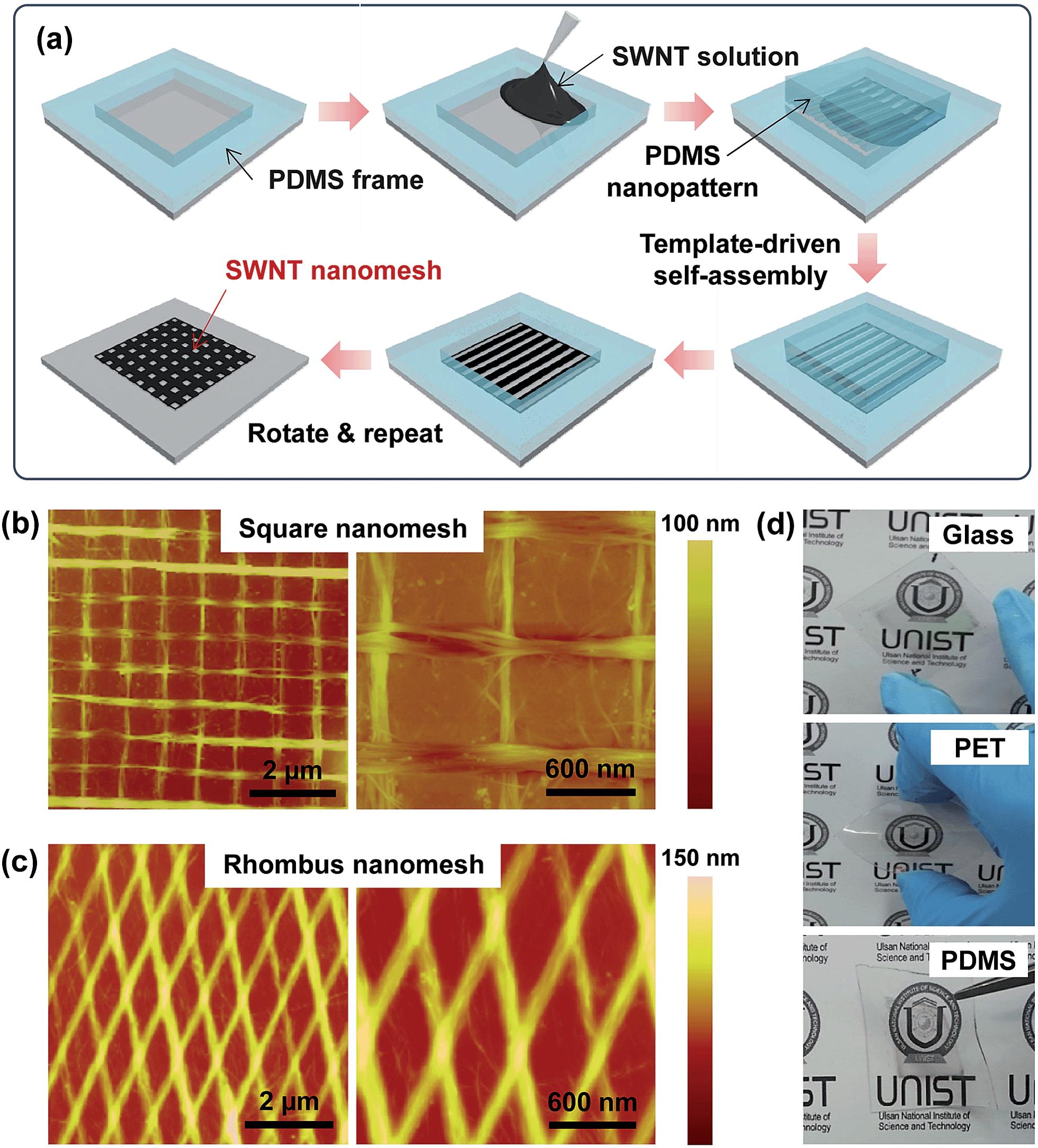 | ||
| Fig. 1 Schematic illustrations and AFM images of SWNT nanomesh films. (a) Schematic representation of the fabrication of the SWNT nanomesh film by template-guided self-assembly. AFM images of 2-bilayer SWNT nanomesh films with (b) square and (c) rhombus structures. (d) The photographs of SWNT nanomesh electrodes on glass, PET, and PDMS substrates. | ||
Chemical doping of SWNT films
To increase the conductivity of SWNT films, we used a nitric acid vapor doping method according to previous literature.55,56 For the nitric acid vapor doping, SWNT films were exposed to nitric acid vapor (15 M) at 90 °C for 1 h in a closed container. After nitric acid vapor doping, the sheet resistance of SWNT films was reduced by 6 times (Fig. S5†).Fabrication of stretchable electrodes
To fabricate the stretchable electrodes, the SWNT nanomesh films were transferred from the glass substrates onto PDMS substrates. In this process, the substrate-mounted nanomesh films were attached onto the PDMS substrates and soaked in acetone to dissolve the PMMA layer between the SWNT film and glass substrate. By soaking the nanomesh SWNT films deposited onto glass in acetone, the entire area of the nanomesh SWNT films could be transferred easily from the glass substrate to the PDMS substrate.Characterization of SWNT films
The surface morphology of the patterned SWNT films was analyzed using scanning electron microscopy (Hitachi S4000) and AFM (Veeco Dimension 3000). The sheet resistance of the SWNT films was measured by the four-point probe method (Keithley 2400). To measure the stretchability, the resistance change as a function of tensile strain was measured by the two-point probe method while stretching the SWNT films on PDMS with a stretching tester (Junil Tech JiBT-200). The optical transparency of the SWNT films was measured using a UV-visible spectrophotometer (Jasco V-670).Results and discussion
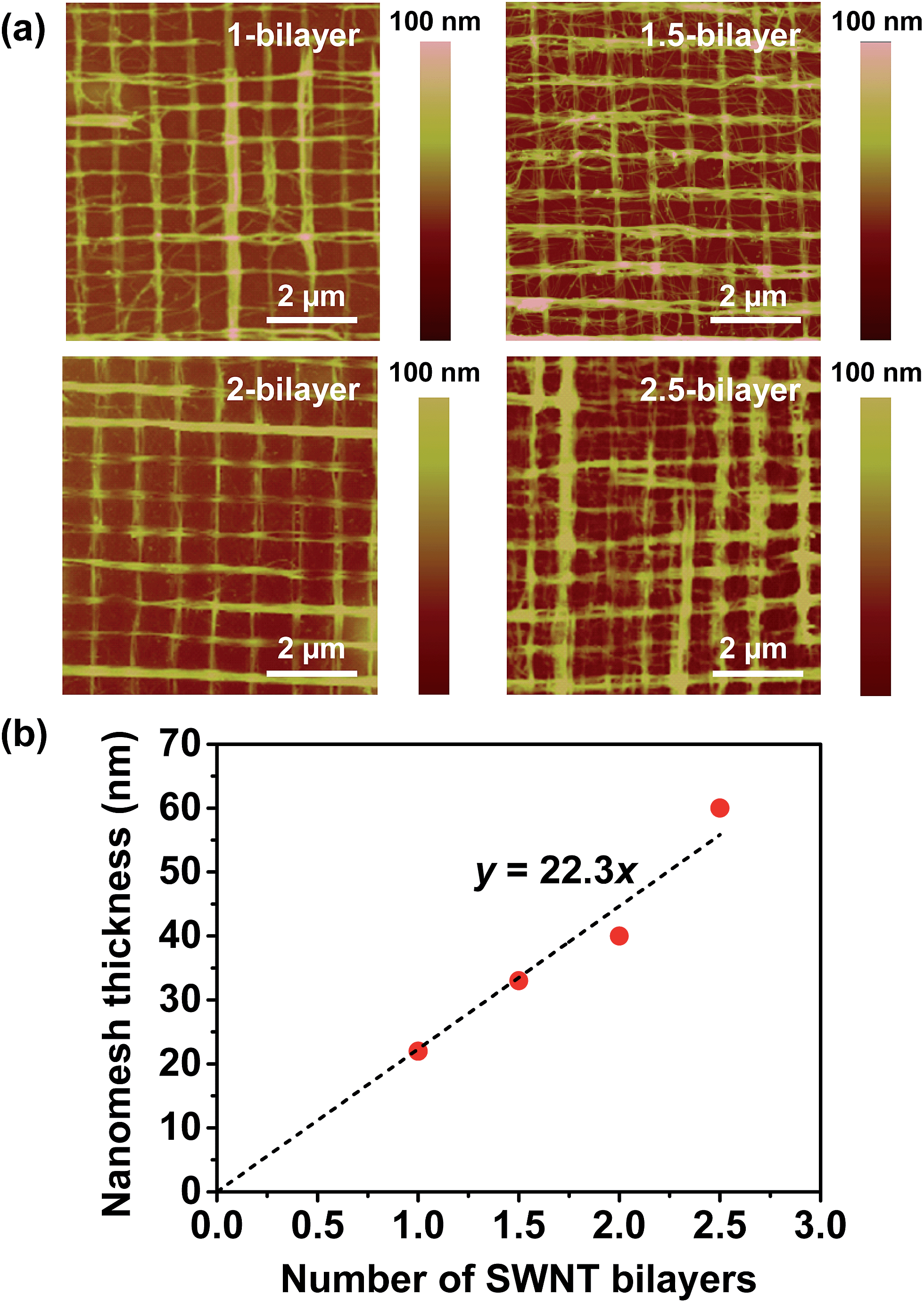
To fabricate the rhombic nanomesh patterns, highly aligned SWNT arrays were first fabricated by the template-guided self-assembly of SWNTs. The evaporation of a physically confined SWNT solution between the PDMS nano-pattern and the substrate resulted in the self-assembly of the SWNTs into a highly aligned array. This template-guided self-assembly process was repeated in the transverse direction to the previously deposited array to fabricate a 2D nanomesh pattern (Fig. 1a). Fig. 1b and c show atomic force microscopy (AFM) images of the SWNT networks. The uniformly aligned SWNTs are organized into overlapping arrays with both square (Fig. 1b) and rhombic (Fig. 1c) nanomesh geometries. The 2D nanomesh pattern can be fabricated on different substrates for the transparent SWNT nanomesh films on glass, polyethylene terephthalate (PET), and PDMS substrates (Fig. 1d).One of the advantages of the template-guided assembly process is the facile control of the mesh structure and overall thickness via repeated LbL processes. In our LbL process, a “1-bilayer” is a nanomesh of crossed SWNT layers after two consecutive perpendicular layer depositions. The addition of a third layer onto the “1-bilayer” square nanomesh results in a “1.5-bilayer” nanomesh. Fig. 2a shows AFM images of LbL-assembled SWNT nanomesh patterns deposited onto glass substrates. We noted that the repeated LbL processes resulted in the formation of a uniform square nanomesh of aligned and crossed SWNTs. Since the LbL process is based on the template-guided self-assembly of CNTs, CNTs tend to be confined by the patterned concave areas of the PDMS stamp and the pre-deposited CNT convex pattern areas, resulting in uniform CNT arrays. In addition, the thickness of the SWNT nanomesh films can be systematically controlled through the number of LbL deposition cycles. As can be seen in Fig. 2b, the thickness of the nanomesh film increased linearly with the number of deposition cycles. This linear relationship gave a slope of 22.3, indicating that the film thickness increased by 22.3 nm with each LbL bilayer.
 | ||
| Fig. 2 Morphology and thickness of LbL assembled SWNT nanomesh films. (a) AFM images of SWNT nanomesh films with different LbL deposition cycles. (b) Thickness of SWNT nanomesh films as a function of the number of SWNT bilayers. | ||
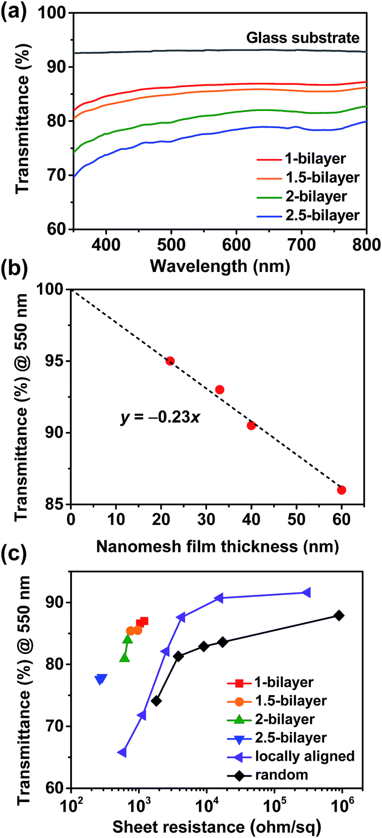
To evaluate the performance of the SWNT nanomesh films as transparent electrodes, we measured their optical transmittance and sheet resistance. Fig. 3a shows that the transmittance of the SWNT nanomesh films (including the glass substrate) decreased with the number of deposition cycles; the transmittance at a wavelength of 550 nm was 87% for a 1-bilayer film and 78% for a 2.5-bilayer film. The decrease in the transmittance of the SWNT nanomesh films with the number of deposition cycles is attributed to the increase in the film thickness. Without the contribution of the original glass substrate (92% transmittance), the transmittance of the 1-bilayer SWNT nanomesh film was 95%, which decreased to 86% at 2.5-bilayers (Fig. 3b). The transmittance decreases linearly with the number of LbL deposition cycles with a slope of −0.23; this demonstrates that the transmittance can be precisely controlled by selecting the number of LbL deposition cycles. Here, the 10 nm increase of nanomesh film thickness results in 2.3% decrease of optical transmittance.
 | ||
| Fig. 3 Transmittance and sheet resistance of SWNT nanomesh films. (a) Optical transmittance of SWNT nanomesh films. (b) The transmittance of SWNT nanomesh films without the contribution of the original glass substrates at 550 nm wavelength. (c) The transmittance and sheet resistance of various SWNT networks with surface geometries of nanomesh, random, and locally aligned networks. | ||
To compare the performance of our nanomesh films to other SWNT-based films with different surface morphologies, we fabricated two different irregular SWNT films lacking the nanomesh structure. The first incorporated a random SWNT network fabricated by transferring a vacuum-filtered SWNT film onto a glass substrate. The other is consisted of locally aligned SWNT films fabricated by spin coating a SWNT solution onto a glass substrate. Fig. S6† shows representative AFM images of the SWNT films with locally aligned and randomly deposited morphologies. Fig. 3c shows the transmittance and sheet resistance of the SWNT nanomesh films, random-network films, and locally aligned films deposited on glass substrates. At similar transmittance values, the sheet resistance was the lowest in the nanomesh films, followed by the locally aligned and random network films. For the 1-bilayer SWNT nanomesh films, the sheet resistance was 1200 Ω sq−1 at 87% transmittance at 550 nm. With an increase in the number of layer-deposition cycles, both the sheet resistance and transmittance continuously decreased. For the 2.5-bilayer SWNT nanomesh films, the sheet resistance decreased to 264 Ω sq−1 at 78% transmittance, which is about 10 and 7 times lower than those of random and locally aligned SWNT networks, respectively, at similar transmittance. This significant decrease in sheet resistance at similar transmittance values for the regular-nanomesh films can be attributed to the reduced inter-tube contact resistance between SWNTs compared to the random network films. Similarly, the locally aligned SWNT films show lower sheet resistances than those of the random SWNT network films. In addition to the low sheet resistance and high transparency, good stretchability is a critical requirement for stretchable optoelectronic applications. To fabricate stretchable electrodes, the SWNT nanomesh films were transferred from the glass substrates onto PDMS substrates.
In the stretchability test of the regular nanomesh structures, the stretching direction with respect to the orientation of the nanomesh structure is critical for the film's stretchability (Fig. 4a). When the stretching direction is parallel to the side of the square-shaped nanomesh structure, the square shape deforms into a rectangular shape, and the assembled SWNT side lines subsequently break with the increase in tensile strain. On the other hand, when the stretching direction is diagonal to the square-shaped nanomesh structure, the square shape deforms into a rhombus shape that can accommodate higher tensile strain without breakage of the SWNT side lines.49–51 In this case, the applied stress is concentrated on the joint areas in the nanomesh networks, leading to reduced breakage of the SWNT side lines. Fig. 4b–d show AFM images of nanomesh films on stretched PDMS substrates. Stretching in a parallel direction results in deformation into a rectangular shape with irregular delamination and breakage of the SWNT lines (white arrows, Fig. 4c). Stretching in a diagonal direction results in deformation into a rhombic shape with minimal delamination or breakage of the SWNT lines (Fig. 4d). Fig. 4e shows the relative resistance change (ΔR/R0) in the SWNT films as a function of tensile strain. The stretchability of the nanomesh films in the diagonal direction was significantly larger than those in the parallel direction and in the random-network films. Under diagonal stretching, the SWNT nanomesh film showed a 35% increase in resistance at 30% strain, which was about 4.7 and 7.7 times lower than those of nanomesh films in the parallel direction (163% increase at 30% strain) and in the randomly networked films (269% increase at 30% strain), respectively.
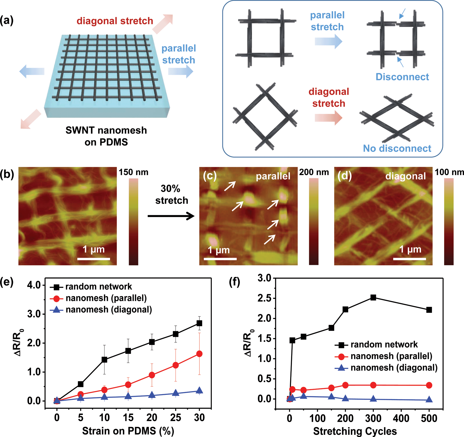 | ||
| Fig. 4 Stretchability of SWNT nanomesh films on PDMS substrates. (a) Schematic of stretching SWNT nanomesh films in parallel and diagonal directions. (b–d) AFM images of the SWNT nanomesh structure on PDMS before (b) and after stretching of the nanomesh in the parallel (c) and diagonal (d) directions. (e) Variations in resistance of SWNT networks as a function of tensile strain. (f) Durability of SWNT nanomesh films as a function of stretching (30% strain) cycles. All the nanomesh and random SWNT films have similar optical transmittances (∼83%). | ||
As can be seen in Fig. S7,† this stretchability (35% increase in resistance at 30% strain) is comparable to the performances of recent transparent electrodes achieved with hierarchical reticulate structures (125% increase in resistance at 60% strain)57 and wrinkled networks (71% increase in resistance at 50% strain)32 of carbon nanotubes. Although Ag nanowires show low resistance at high transparency, most of the studies show large resistance increase (200–600% increase in resistance at about 30% strain) with the tensile strain.28,48,58 The enhanced stretchability of the nanomesh films in the diagonal direction is attributable to the deformation of the rhombic shapes, which can accommodate large tensile strains. For larger tensile strains, we observed that the nanomesh films in the diagonal direction can be stretched up to 100% with 530% increase in resistance (Fig. S8†).
In addition to the stretchability, the nanomesh films exhibited enhanced durability in the diagonal direction. Fig. 4f shows the change in the initial resistance (R0) of the SWNT films as a function of the number of stretching cycles. While the nanomesh films stretched in the diagonal direction showed a negligible change (less than 6%) in R0 during 500 stretching cycles at a strain of 30%, R0 increased by about 34% in the nanomesh films stretched in the parallel direction and 252% in the random-network films. An AFM analysis of the nanomesh films performed after the repeated stretching cycles confirms that the conductive nanomesh structures were better maintained in the nanomeshes stretched in the diagonal direction compared to the parallel direction (Fig. S9†). Since a square is a rhombus with 90 degree angles for all of its interior angles, we also investigated the effects of the interior angles of the rhombic nanomesh films on the stretchability. The different interior angles (145 and 90 degrees) in the rhombus nanomesh films produced similar stretching capability (Fig. S10†), indicating a minimal effect of the interior angles of the rhombic structure on the stretchability. The mechanical robustness with respect to stretching was also confirmed by the hysteresis curves of the SWNT films. Fig. S11† shows that the rhombus nanomesh films show less hysteresis and better persistence of electrical conductivity after repeated stretching and relaxation (to 30% strain) than the random-network film and the square nanomesh film pulled in the parallel direction.
As a further demonstration of the stretchability of the nanomesh films, green LED light was wired to the SWNT films, and the LED brightness was measured as a function of tensile strain at a constant applied voltage of 1.5 V. Fig. 5a and b show the change in LED brightness provided by the nanomesh and random SWNT films with increasing tensile strain up to 30%. In this test, we used nanomesh and random SWNT films with almost the same transmittance (≈83%), which resulted in different sheet resistances: ∼1 kΩ sq−1 for the nanomesh films and ∼9 kΩ sq−1 for the random SWNT films. At the same transmittance, the nanomesh films provided a higher initial LED brightness than the random films (Fig. 5c). For both the nanomesh and random SWNT films, the LED brightness decreased linearly with the increase in tensile strain. When we compared the relative change in LED power, the nanomesh SWNT films showed a decrease in LED power about two times smaller than that of the random SWNT films (Fig. 5d).
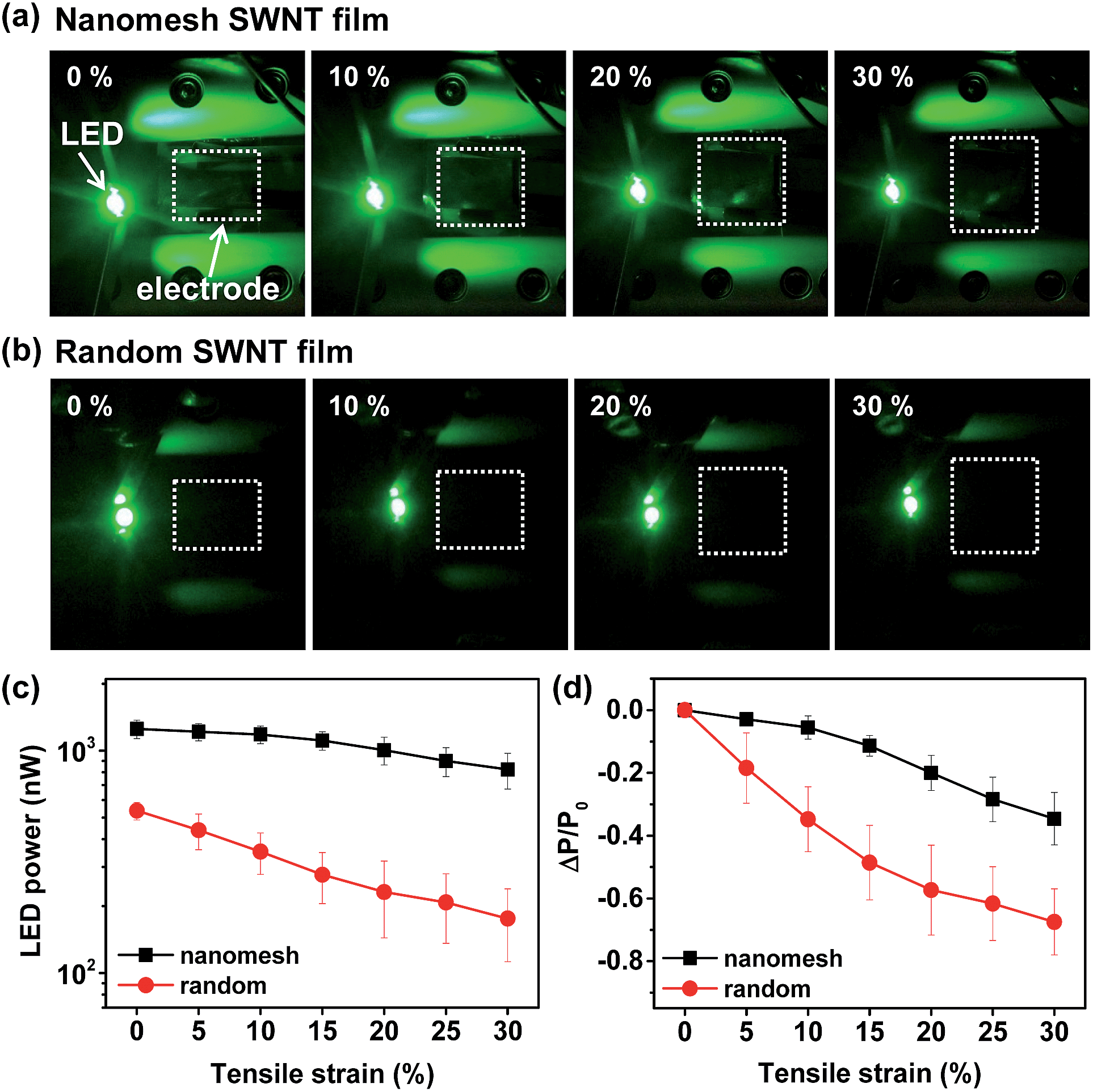 | ||
| Fig. 5 Stretchable SWNT electrodes for LED lighting. Photographs of LED brightness as a function of tensile strain for SWNT (a) nanomesh and (b) random films. The white squares indicate the SWNT films. (c) Variations of LED brightness power and (d) relative change in LED power for SWNT nanomesh and random films as a function of tensile strain. | ||
Conclusions
In summary, we developed a layer-by-layer template-guided process for the self-assembly of carbon nanotubes into 2D rhombic nanomesh films for use in transparent and stretchable electrodes. Compared to random-network carbon-nanotube films, the rhombic nanomesh films showed a significantly lower sheet resistance, greater stretchability, and better mechanical durability. The enhanced performance of the rhombic nanomesh films in transparent and stretchable electrodes is attributable to the greater deformability of the rhombic structure and the lower electrical percolation threshold of regular mesh networks. By altering the size and shape of the template pattern and using different types of carbon nanotubes such as double-walled carbon nanotubes with lower sheet resistance,59 this assembly method can be further tuned to obtain the optimum properties for applications requiring transparent and stretchable electrodes.Acknowledgements
This work was supported by the National Research Foundation of Korea (NRF-2011-0014965, NRF-2014M3C1B2048198) and Korea Institute of Science and Technology (KIST) (2E22112-11-249).Notes and references
- P. Blake, P. D. Brimicombe, R. R. Nair, T. J. Booth, D. Jiang, F. Schedin, L. A. Ponomarenko, S. V. Morozov, H. F. Gleeson and E. W. Hill, Nano Lett., 2008, 8, 1704 CrossRef PubMed.
- R. C. Y. King and F. Roussel, Appl. Phys. A, 2007, 86, 159 CrossRef CAS.
- D. S. Hecht, D. Thomas, L. Hu, C. Ladous, T. Lam, Y. Park, G. Irvin and P. Drzaic, J. Soc. Inf. Disp., 2009, 17, 941 CrossRef CAS.
- S. Bae, H. Kim, Y. Lee, X. Xu, J.-S. Park, Y. Zheng, J. Balakrishnan, T. Lei, H. R. Kim and Y. I. Song, Nat. Nanotechnol., 2010, 5, 574 CrossRef CAS PubMed.
- A. R. Madaria, A. Kumar and C. Zhou, Nanotechnology, 2011, 22, 245201 CrossRef PubMed.
- N. Fukaya, D. Y. Kim, S. Kishimoto, S. Noda and Y. Ohno, ACS Nano, 2014, 8, 3285 CrossRef CAS PubMed.
- J. Wu, M. Agrawal, H. A. Becerril, Z. Bao, Z. Liu, Y. Chen and P. Peumans, ACS Nano, 2009, 4, 43 CrossRef PubMed.
- D. Zhang, K. Ryu, X. Liu, E. Polikarpov, J. Ly, M. E. Tompson and C. Zhou, Nano Lett., 2006, 6, 1880 CrossRef CAS PubMed.
- M. W. Rowell, M. A. Topinka, M. D. McGehee, H.-J. Prall, G. Dennler, N. S. Sariciftci, L. Hu and G. Gruner, Appl. Phys. Lett., 2006, 88, 233506 CrossRef PubMed.
- X. Wang, L. Zhi and K. Müllen, Nano Lett., 2008, 8, 323 CrossRef CAS PubMed.
- B. G. Lewis and D. C. Paine, MRS Bull., 2000, 25, 22 CrossRef CAS.
- T. Minami, Thin Solid Films, 2008, 516, 1314 CrossRef CAS PubMed.
- K. Ellmer, Nat. Photonics, 2012, 6, 809 CrossRef CAS.
- D. S. Hecht, L. Hu and G. Irvin, Adv. Mater., 2011, 23, 1482 CrossRef CAS PubMed.
- M. Kaempgen, C. K. Chan, J. Ma, Y. Cui and G. Gruner, Nano Lett., 2009, 9, 1872 CrossRef CAS PubMed.
- Z. Wu, Z. Chen, X. Du, J. M. Logan, J. Sippel, M. Nikolou, K. Kamaras, J. R. Reynolds, D. B. Tanner and A. F. Hebard, Science, 2004, 305, 1273 CrossRef CAS PubMed.
- L. Hu, H. S. Kim, J.-Y. Lee, P. Peumans and Y. Cui, ACS Nano, 2010, 4, 2955 CrossRef CAS PubMed.
- L. Hu, H. Wu and Y. Cui, MRS Bull., 2011, 36, 760 CrossRef CAS.
- A. R. Rathmell and B. J. Wiley, Adv. Mater., 2011, 23, 4798 CrossRef CAS PubMed.
- T. He, A. Xie, D. H. Reneker and Y. Zhu, ACS Nano, 2014, 8, 4782 CrossRef CAS PubMed.
- J.-Y. Lee, S. T. Connor, Y. Cui and P. Peumans, Nano Lett., 2008, 8, 689 CrossRef CAS PubMed.
- S. Morozov, K. Novoselov, M. Katsnelson, F. Schedin, D. Elias, J. Jaszczak and A. Geim, Phys. Rev. Lett., 2008, 100, 016602 CrossRef CAS.
- J. K. Wassei and R. B. Kaner, Mater. Today, 2010, 13, 52 CrossRef CAS.
- Y. H. Ha, N. Nikolov, S. K. Pollack, J. Mastrangelo, B. D. Martin and R. Shashidhar, Adv. Funct. Mater., 2004, 14, 615 CrossRef CAS.
- S. Kirchmeyer and K. Reuter, J. Mater. Chem., 2005, 15, 2077 RSC.
- T. Sekitani, H. Nakajima, H. Maeda, T. Fukushima, T. Aida, K. Hata and T. Someya, Nat. Mater., 2009, 8, 494 CrossRef CAS PubMed.
- Z. Yu, X. Niu, Z. Liu and Q. Pei, Adv. Mater., 2011, 23, 3989 CrossRef CAS PubMed.
- J. Liang, L. Li, X. Niu, Z. Yu and Q. Pei, Nat. Photonics, 2013, 7, 817 CrossRef CAS.
- M. Kaltenbrunner, M. S. White, E. D. Głowacki, T. Sekitani, T. Someya, N. S. Sariciftci and S. Bauer, Nat. Commun., 2012, 3, 770 CrossRef PubMed.
- D. H. Kim, J. Xiao, J. Song, Y. Huang and J. A. Rogers, Adv. Mater., 2010, 22, 2108 CrossRef CAS PubMed.
- K. Liu, Y. Sun, P. Liu, X. Lin, S. Fan and K. Jiang, Adv. Funct. Mater., 2011, 21, 2721 CrossRef CAS.
- D. J. Lipomi, M. Vosgueritchian, B. C. Tee, S. L. Hellstrom, J. A. Lee, C. H. Fox and Z. Bao, Nat. Nanotechnol., 2011, 6, 788 CrossRef CAS PubMed.
- T. Yamada, Y. Hayamizu, Y. Yamamoto, Y. Yomogida, A. Izadi-Najafabadi, D. N. Futaba and K. Hata, Nat. Nanotechnol., 2011, 6, 296 CrossRef CAS PubMed.
- J. Park, Y. Lee, J. Hong, M. Ha, Y.-D. Jung, H. Lim, S. Y. Kim and H. Ko, ACS Nano, 2014, 8, 4689 CrossRef CAS PubMed.
- K. Takei, T. Takahashi, J. C. Ho, H. Ko, A. G. Gillies, P. W. Leu, R. S. Fearing and A. Javey, Nat. Mater., 2010, 9, 821 CrossRef CAS PubMed.
- P. Lee, J. Lee, H. Lee, J. Yeo, S. Hong, K. H. Nam, D. Lee, S. S. Lee and S. H. Ko, Adv. Mater., 2012, 24, 3326 CrossRef CAS PubMed.
- C. Yu, C. Masarapu, J. Rong, B. Wei and H. Jiang, Adv. Mater., 2009, 21, 4793 CrossRef CAS PubMed.
- F. Xu and Y. Zhu, Adv. Mater., 2012, 24, 5117 CrossRef CAS PubMed.
- D.-H. Kim, J. Song, W. M. Choi, H.-S. Kim, R.-H. Kim, Z. Liu, Y. Y. Huang, K.-C. Hwang, Y.-w. Zhang and J. A. Rogers, Proc. Natl. Acad. Sci. U. S. A., 2008, 105, 18675 CrossRef CAS PubMed.
- S. Xu, Y. Zhang, J. Cho, J. Lee, X. Huang, L. Jia, J. A. Fan, Y. Su, J. Su and H. Zhang, Nat. Commun., 2013, 4, 1543 CrossRef PubMed.
- G. S. Jeong, D.-H. Baek, H. C. Jung, J. H. Song, J. H. Moon, S. W. Hong, I. Y. Kim and S.-H. Lee, Nat. Commun., 2012, 3, 977 CrossRef PubMed.
- H. Wu, M. Menon, E. Gates, A. Balasubramanian and C. J. Bettinger, Adv. Mater., 2014, 26, 706 CrossRef CAS PubMed.
- J. Park, S. Wang, M. Li, C. Ahn, J. K. Hyun, D. S. Kim, D. K. Kim, J. A. Rogers, Y. Huang and S. Jeon, Nat. Commun., 2012, 3, 916 CrossRef PubMed.
- W. Hu, X. Niu, L. Li, S. Yun, Z. Yu and Q. Pei, Nanotechnology, 2012, 23, 344002 CrossRef PubMed.
- C. F. Guo, T. Sun, Q. Liu, Z. Suo and Z. Ren, Nat. Commun., 2014, 5, 3121 Search PubMed.
- F. Farukh, E. Demirci, M. Acar, B. Pourdeyhimi and V. V. Silberschmidt, J. Mater. Sci., 2014, 49, 4081 CrossRef CAS.
- H. Y. Jang, S.-K. Lee, S. H. Cho, J.-H. Ahn and S. Park, Chem. Mater., 2013, 25, 3535 CrossRef CAS.
- J. Liang, L. Li, K. Tong, Z. Ren, W. Hu, X. Niu, Y. Chen and Q. Pei, ACS Nano, 2014, 8, 1590 CrossRef CAS PubMed.
- T. Someya, Y. Kato, T. Sekitani, S. Iba, Y. Noguchi, Y. Murase, H. Kawaguchi and T. Sakurai, Proc. Natl. Acad. Sci. U. S. A., 2005, 102, 12321 CrossRef CAS PubMed.
- D. H. Kim and J. A. Rogers, Adv. Mater., 2008, 20, 4887 CrossRef CAS.
- T. Takahashi, K. Takei, A. G. Gillies, R. S. Fearing and A. Javey, Nano Lett., 2011, 11, 5408 CrossRef CAS PubMed.
- I. Jurewicz, P. Worajittiphon, A. A. King, P. J. Sellin, J. L. Keddie and A. B. Dalton, J. Phys. Chem. B, 2011, 115, 6395 CrossRef CAS PubMed.
- H. Ko, S. Peleshanko and V. V. Tsukruk, J. Phys. Chem. B, 2004, 108, 4385 CrossRef CAS.
- H. Ko and V. V. Tsukruk, Nano Lett., 2006, 6, 1443 CrossRef CAS PubMed.
- H.-Z. Geng, K. K. Kim, K. P. So, Y. S. Lee, Y. Chang and Y. H. Lee, J. Am. Chem. Soc., 2007, 129, 7758 CrossRef CAS PubMed.
- H. Gao, R. Izquierdo and V.-V. Truong, Chem. Phys. Lett., 2012, 546, 109 CrossRef CAS PubMed.
- L. Cai, J. Li, P. Luan, H. Dong, D. Zhao, Q. Zhang, X. Zhang, M. Tu, Q. Zeng and W. Zhou, Adv. Funct. Mater., 2012, 22, 5238 CrossRef CAS.
- H. Lee, K. Lee, J. T. Park, W. C. Kim and H. Lee, Adv. Funct. Mater., 2014, 24, 3276 CrossRef CAS.
- F. Mirri, A. W. Ma, T. T. Hsu, N. Behabtu, S. L. Eichmann, C. C. Young, D. E. Tsentalovich and M. Pasquali, ACS Nano, 2012, 6, 9737 CrossRef CAS PubMed.
Footnotes |
| † Electronic supplementary information (ESI) available. See DOI: 10.1039/c4tc02733g |
| ‡ These authors contributed equally to this work. |
| This journal is © The Royal Society of Chemistry 2015 |