
 Open Access Article
 This Open Access Article is licensed under a
 Creative Commons Attribution 3.0 Unported Licence
Atomic layer deposition of B-doped ZnO using triisopropyl borate as the boron precursor and comparison with Al-doped ZnO†
Diana
Garcia-Alonso
 a,
Stephen E.
Potts
ab,
Cristian A. A.
van Helvoirt
a,
Marcel A.
Verheijen
a and
Wilhelmus M. M.
Kessels
*ac
a,
Stephen E.
Potts
ab,
Cristian A. A.
van Helvoirt
a,
Marcel A.
Verheijen
a and
Wilhelmus M. M.
Kessels
*ac
aDepartment of Applied Physics, Eindhoven University of Technology, P. O. Box 513, 5600 MB Eindhoven, The Netherlands. E-mail: w.m.m.kessels@tue.nl; Tel: +31-40-247-3477
bSchool of Biological & Chemical Sciences, Queen Mary University of London, Mile End Road, E1 4NS, UK
cSolliance Solar Research, High Tech Campus 5, 5656AE Eindhoven, The Netherlands
First published on 5th February 2015
Abstract
Doped ZnO films are an important class of transparent conductive oxides, with many applications demanding increased growth control and low deposition temperatures. Therefore, the preparation of B-doped ZnO films by atomic layer deposition (ALD) at 150 °C was studied. The B source was triisopropyl borate, B(OiPr)3 (TIB), which has a significantly lower vapour pressure and is a safer alternative precursor to highly toxic diborane(6), B2H6. The doping fraction (DF) of the films was varied by the ratio of ZnO and dopant ALD cycles. The electrical, structural and optical properties of the ZnO:B films were studied as a function of the dopant concentration and deposition temperature, and were compared with ZnO:Al films, where dimethylaluminium isopropoxide, [Al(CH3)2(OiPr)]2 (DMAI) and trimethylaluminium, Al2(CH3)6 (TMA) were the Al sources. A low resistivity of 3.5 mΩ cm was achieved for 45 nm-thick ZnO:B deposited at 150 °C with a doping fraction (DF) of 0.016, which was similar to the results obtained for ZnO:Al films prepared with DMAI and lower compared to the 8 mΩ cm achieved for ZnO:Al prepared with TMA at an optimized DF of 0.040. Hence TIB, as well as DMAI, outperformed the conventionally employed TMA in terms of doping efficiency at 150 °C. It was found that the optical band gap could be easily tuned over the range of ∼3.2–3.7 eV by modifying the doping fraction.
1 Introduction
Tin-doped indium oxide (ITO) is the most popular transparent conductive oxide (TCO) for optoelectronic devices, but the scarcity and relative expense of indium has led to alternative TCO materials being sought.1,2 ZnO has many intrinsic properties that makes it a good candidate for a TCO material as it has a direct wide band gap of ∼3.4 eV, a refractive index of ∼2.0 and electron mobilities as high as 50–60 cm2 V−1 s−1.3–6 ZnO films exhibit good optical transparency below the band gap and their conductivity can be increased by doping with a group 13 element (i.e., ZnO:X where X = Al, B, Ga, In).7,8ZnO (either intrinsic, i.e. without intentional doping, or doped) is especially of interest for application fields with very strict cost requirements, such as the field of photovoltaics (PV). For example, ZnO is employed on the front and/or rear of silicon heterojunction (SHJ) solar cells,9–11 used as multifunctional front contact on thin film solar cells such as amorphous silicon, Cu(In,Ga)(S,Se)2 (CIGS), CdTe, or organic solar cells,6,12,13 or it acts as a buffer layer or semi-transparent cathode in organic photovoltaics (OPV)14,15 or as a nanostructured photoanode or interlayer in dye-sensitised solar cells (DSCs).16,17
For many TCO applications, particularly in PV, ultrathin (doped) ZnO films with a low resistivity (<1 mΩ cm) and a high transparency (>80%) in the spectral region of interest are required.6,18 Preferably, the low resistivity should be a result of high carrier mobility rather than high free-electron density, the latter resulting in a decrease in transparency, especially in the infrared region.19 Low deposition temperatures (<200 °C) and a tuneable roughness are other requirements for certain types of solar cells, such as CIGS, flexible plastic DSCs and SHJ cells.
ZnO and doped ZnO thin films have been grown by various methods such as spray pyrolysis,20,21 sol–gel deposition,22,23 sputtering,24,25 pulsed laser deposition (PLD),25,26 chemical bath deposition (CBD),27,28 metal–organic chemical vapour deposition (MOCVD),29,30 and atomic layer deposition (ALD).12–14,31,32 ALD, in particular, is becoming a popular deposition technique as it allows for deposition at low temperatures, it is a ‘soft’ method without highly energetic species and it is scalable. Furthermore, the fact that ALD operates via self-limiting surface reactions in cycles means that doping materials can be introduced with greater control and tuning than other deposition methods. Recent reviews emphasise the potential of ALD to contribute towards achieving high-efficiency solar cells.33,34
Many articles have been published on the ALD of intrinsic ZnO and ZnO:Al, mostly using TMA as an Al source, but far fewer using other dopant materials. TMA is a highly reactive molecule, which has led to its popularity as an ALD precursor. However, this high reactivity can lead to difficulty in controlling doping levels. Furthermore, it is pyrophoric, making it potentially difficult to handle and dangerous in high quantities such as those used in high-volume manufacturing. In this article, we investigate the ALD of ZnO:B using an alternative B source, triisopropyl borate (TIB), in conjunction with a ZnO ALD process comprising diethylzinc (DEZ) and H2O half-cycles. First, a brief review of the state-of-the-art of ALD ZnO:X (X = Al, B) and the precursors used to date is reported. Second, the electronic, structural and optical properties of the ZnO:B films obtained using TIB are presented and compared with the properties of the ZnO:Al films obtained using conventional TMA and alternative DMAI precursors under the same conditions.35,36
2 ALD of ZnO:X and precursors
ALD is an ultrathin film deposition technique comprising alternating exposures of gaseous precursors, known as half-cycles, to a surface (substrate) separated by purging steps to ensure the precursors do not mix.37,38 ALD excels in producing highly uniform and conformal films with a precise growth control and is compatible with deposition temperatures from room temperature up to ∼350 °C,39–41 where the higher end of the temperature range is limited by the decomposition temperature of the metal–organic precursor.40–42 The cyclic nature of ALD means that doses of dopant sources can easily be incorporated into the process. The technique also allows for the deposition of virtually defect-free films with tailored compositions (via doping) and it can easily be used to produce multilayer structures.43–47 Doping is often achieved by combining the steps of two normal ALD processes in a supercycle, where m cycles of the base material process (in this case ZnO) are followed by one cycle of the doping material (Fig. 1). The number of cycles m is chosen to obtain the desired film composition, and the supercycle (m + 1) is repeated x times until the desired film thickness is reached. The value of m can also be varied in the supercycles throughout the deposition process in order to obtain films with graded doping.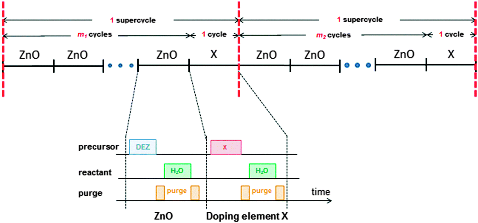 | ||
| Fig. 1 A schematic representation of two ALD supercycles used to dope the ZnO films with a doping element, X (X = Al, B, Ga, etc.). For uniform doping, a constant value of m is used (m1 = m2 =⋯= mn) whereas for films with graded doping, the value of m can be varied. Details of the ALD processes are shown in the lower part of the figure: the process for the ZnO based material comprises two half-cycles in which DEZ and H2O are dosed; in most cases, the ALD process of the doping material also comprises two doses: dopant precursor dosing and H2O dosing. Other co-reactants such as O3 or O2 plasma can also be employed instead of H2O, for both the ZnO and the doping element. | ||
A wide selection of elements with a different valency to Zn can be used to dope ZnO, such as Al, B, Ga, Ge, H, Hf, Mn, N, P, S, Si, Sn, Ti, and Zr. A complete review of doping materials for ZnO by ALD can be found in the recently published review by Tynell et al.32
Reported ALD processes for ZnO:X (X = Al, B) are summarised in Table 1. In almost all cases of ZnO ALD, DEZ is used as the Zn source. The most commonly-employed dopant is Al and the most frequently used Al-source for the ALD of ZnO:Al is trimethylaluminium (TMA), as evidenced by the large number of publications reporting it.8,43,44,48–77 The main reason behind this is that TMA is a well-documented precursor and is extensively used within the ALD community. However, TMA is a highly volatile molecule39,78 and it is very reactive towards a variety of surface groups, which is ideal for pure Al2O3 ALD processes but that can make doping using ALD difficult to control because it is too reactive to afford a sufficiently low surface density of Al atoms. Aluminium isopropoxide (AIP) has also been reported as an alternative Al source in the ALD of ZnO:Al,79 where its potential advantage is that AIP is less reactive than TMA towards surface groups, which makes doping potentially easier to control. However, AIP is a solid at room temperature and exists as a tetramer.80 Consequently, the low volatility of AIP could prove to be challenging in some ALD systems as it can require heating up to ∼130 °C before an optimum vapour pressure for growth is obtained. A compromise in reactivity and volatility between TMA and AIP can be found in the heteroleptic precursor dimethylaluminium isopropoxide, [AlMe2(OiPr)]2 (DMAI), which has been employed as an ALD precursor to both Al2O381,82 and ZnO:Al thin films.36,83 We recently reported the ALD of ZnO:Al using DMAI, which led to higher doping efficiencies (i.e., higher active dopant densities) and lower resistivities than those obtained when TMA was used.36 This improved doping efficiency resulted from a lower surface density of Al atoms due to the lower reactivity of DMAI and the steric hindrance caused by the bulky OiPr ligands on the precursor.
| Material | Zn source | Dopant source | Co-reactant | Ref. |
|---|---|---|---|---|
| a Me = methyl, CH3; Et = ethyl, CH2CH3; iPr = isopropyl, CH(CH3)2. | ||||
| ZnO:Al | ZnEt2 | [AlMe3]2 | H2O | 8, 43, 44, 48–76 and this work |
| O3 | 77 | |||
| [Al(OiPr)3]4 | H2O | 79 | ||
| [AlMe2(OiPr)]2 | H2O | 36, 83 and this work | ||
| ZnMe2 | [AlMe3]2 | H2O | 48 | |
| [ZnMe(OiPr)]4 | [AlMe2(OiPr)]2 | H2O | 84 | |
| ZnO:B | ZnEt2 | B2H6 | H2O | 85–88 |
| B(OiPr)3 | H2O | This work | ||
The most commonly reported B source for thin film deposition is diborane(6) (B2H6), which is an extremely flammable gas at room temperature. It is also highly toxic89 and is consequently typically used as a 1–10% solution in H2. B2H6 has been the most widely used as a CVD precursor to ZnO:B90–98 with, to date, relatively few reports of its use in ALD.85–88 We believe that the reason behind this low number of publications on the use of B2H6 for ALD is its extremely high vapour pressure,99 which is not easy to control under ALD conditions. Furthermore, the highly toxic nature of B2H6 means it is undesirable to handle, which has led to alternatives being sought.
Potential candidates for the B source were considered based on the precursors that had been used for CVD of B-containing films. CVD processes using precursors such as borazine,100B,B′,B′′-trichloroborazine101 and tris(dimethylamido)borane102–106 have been reported, although in those cases the target material was BN. Boron tribromide (BBr3) has been used as an ALD precursor to B2O3107 and BN;108 however, bromide impurities in the film can be extremely detrimental to its electrical properties. Specifically concerning ZnO:B, a recent study was carried out in order to investigate safer precursors than B2H6 for CVD,109,110 wherein N,N′,N′′-trimethylborazine, trimethyl borate and triisopropyl borate (TIB) were employed as the B sources. The ZnO:B films deposited using these aforementioned precursors had comparable resistivities to films where B2H6 was used. Based on these results, the selection of a potential B-source candidate for ALD was done for this work. In terms of their use as an ALD precursor, N,N′,N′′-trimethylborazine was not considered because, being isostructural with benzene, it was unclear how it could react with surface groups in an ALD mechanism. Regarding trimethyl borate, its vapour pressure (100 Torr at 20 °C)109 was unpractical. On this basis, TIB was chosen as the most promising ALD precursor for ZnO:B.
We report here the use of TIB as an alternative B precursor for the ALD of ZnO:B and we compare the results with ZnO:Al films deposited using DMAI and TMA as Al sources. We extended the temperature range of the recently reported ZnO:Al ALD process using DMAI36 from 250 °C down to 150 °C in order to compare the film properties given by the two different dopants. A comparison of these two precursors with their more traditional counterparts is given in Table 2. The TIB and DMAI molecules, which contain OiPr ligands, are large compared to TMA. The presence of OiPr results in possible steric hindrance, thus affording a lower surface density of the doping element and hence a better doping efficiency. Additionally, like DMAI, TIB is not pyrophoric, making it safer to handle for high-volume, high-throughput ALD systems, especially operating at atmospheric pressure.111
| Properties | Zn precursor | B precursors | Al precursors | ||
|---|---|---|---|---|---|
| Traditional | New | Traditional | New | ||
| Abbreviation | DEZ | B2H6 | TIB | TMA | DMAI |
| Full name | Diethyl zinc | Diborane(6) | Triisopropyl borate | Trimethyl aluminium | Dimethylaluminium isopropoxide |
| Formula | Zn(CH2CH3)2 | B2H6 | B(OiPr)3 | [Al(CH3)3]2 | [Al(CH3)2(OiPr)]2 |
| Physical state (R.T.P.) | Liquid | Gas | Liquid | Liquid | Liquid |
| Melting point (°C) | −28 | −165109 | n/a | 15 | <RT82 |
| Boiling point (°C) | 117 | −92.5109 | 140109 | 125 | 17282 |
| Decomposition temperature (°C) | ∼280116,117 | >200118 | n/a | ∼330119 | ∼370120 |
| Vapour pressure at 25 °C (Torr) | ∼16121 | ∼35![[thin space (1/6-em)]](https://www.rsc.org/images/entities/char_2009.gif) 40099 40099 |
∼1378 | ∼13121 | 0.85122 |
| Flammability | Highly flammable, pyrophoric | Extremely flammable, non-phyrophoric | Highly flammable, non-phyrophoric | Highly flammable, pyrophoric | Highly flammable, non-pyrophoric |
3 Experimental
The ZnO doping ALD processes were carried out in an open-load ALD reactor (OpAL™, Oxford Instruments), as reported previously.35,36 Samples were deposited with different doping concentrations over a range of substrate temperatures (150–240 °C). 7059 corning glass, silicon wafers with a native oxide layer, and silicon wafers with a 450 nm-thick thermally-grown SiO2 layer were used as substrates. Diethyl zinc (DEZ > 99.999%, Dockweiler Chemicals) and triisopropyl borate (TIB > 98%, Air Liquide) were used as Zn and B-doping precursors respectively. Dimethylaluminium isopropoxide (DMAI > 99.999%, Air Liquide) and trimethyl aluminium (TMA > 99.999%, Air Liquide) were used as reference Al doping precursors. Deionized water vapour (DI-H2O) was used as the co-reactant in all cases. The ZnO:B ALD process details will follow in Section 4.1. The ZnO:Al ALD processes using DMAI and TMA as doping precursors are described elsewhere.35,82Spectroscopic ellipsometry (SE) was used to measure the film thickness and the dielectric function of the films.123 The in situ and ex situ measurements were performed using a Woollam, Inc. M2000 visible and near-infrared ellipsometer (0.75–5 eV). The SE data were analysed using a Drude oscillator model.35
The film compositions (doping and impurity concentrations) were analysed by X-ray photoelectron spectroscopy (XPS Thermo Scientific K-Alpha KA1066, monochromatic Al Kα (hν = 1486.6 eV), X-ray spot: 400 μm). The sensitivity factors used for quantification were: B 1s, 0.470; O 1s, 2.881; Zn 2p3/2, 21.391; Al 2p, 0.75; C 1s, 0.919. Rutherford backscattering spectrometry (RBS; 2 MeV He+ beam in channelling configuration under perpendicular incidence with the detector at 170° scattering angle) and proton-induced gamma ray emission (PIGE; 2700 keV H+ beam with an angle of incidence of 6.5° between the beam and sample surface and the gamma detector at an angle of 90° with respect to the beam) were used to calibrate the sensitivity factors used in XPS quantification and to obtain the areal density of the doping elements. The RBS/PIGE measurements were carried out at AccTec B.V. The film composition is presented as the doping fraction (DF) calculated by  , where X = Al or B.
The resistivity (ρ) and sheet resistance (Rs) of all samples were obtained by four-point probe (4pp) measurements using a Keithley 2400 SourceMeter and a Signaton S-301-6 probe. The carrier concentration (n) was extracted from SE data assuming an effective mass of 0.4 and cross-checked using a Hall measurement system (BIO-RAD) using the van der Pauw configuration. The electron mobility (μ) of the films was calculated following the formula μ = (n·ρ·e)−1, where e is the elementary charge.
The structural properties of the samples were studied by X-ray diffraction (XRD; PanAlytical X'pert PRO MRD) and transmission electron microscopy (TEM; JEOL ARM 200 probe corrected TEM, operated at 200 kV). UV-VIS-NIR spectroscopy (Cary 5000, Agilent Technologies) was used to study the optical transparency of the films. The absorption coefficient (α) was calculated from the extinction coefficient (k) of the films as obtained by the SE data. The optical band gap of the films was calculated using the so-called Tauc plots extracted from the SE data as well.35,124
4 Results and discussion
4.1 Process properties and atomic composition of ALD films
The ZnO doping ALD processes were carried out using so-called supercycles as illustrated in Fig. 1. In principle, the concept of supercycle is effective when the two individual ALD processes (i.e., the base material ALD process and the dopant ALD process) are compatible with each other. Additionally, the ALD supercycle should be in saturation when the two individual ALD processes are in saturation. This is in fact the case for the ZnO and Al2O3 ALD processes used to obtain Al-doped ZnO films that we reported previously.35,36,82Attempts to obtain a B2O3 ALD process using TIB with either water or an O2 plasma as co-reactants resulted in no growth at all temperatures investigated. As part of their studies on the BBr3–H2O ALD process, Putkonen and Niinistö suggested that volatile boric acid, B(OH)3, was formed instead of B2O3 when the boron precursor came into contact with excess water under reduced pressure.107 The boric acid was then carried away in the vacuum rather than being incorporated into a growing film. We believe that a similar mechanism might take place when TIB is the precursor, which would account for the lack of growth of B2O3. However, it was still possible to grow ZnO:B films using TIB incorporated into a supercycle using the DEZ–H2O process. For this reason, the parameters of the ALD process for the B dopant were tuned during the ZnO doping ALD process at 150 °C using a supercycle with m = 4 (i.e., 5 cycles consisting of 4 ZnO + 1 TIB) and using the already-optimised ZnO ALD process parameters (50 ms DEZ dose, 5 s purge, 20 ms H2O dose, 6 s purge).35 For the process development, in situ spectroscopic ellipsometry (SE) was used to measure the film thickness after every supercycle. Growth per supercycle (GPSC) values were determined from the slope of the graphs of the thickness as a function of the number of supercycles (see Fig. S1 of the ESI†). We report here the GPSC rather than the growth per cycle (GPC) for the doping process, as it takes into account possible atypical interactions that might occur between the DEZ–H2O and TIB–H2O ALD processes, for example, nucleation delays or etching.35
The saturation curves for the gas exposures and purges of the B cycle of an ALD supercycle corresponding to four DEZ cycles and one TIB cycle for the ZnO:B process are depicted in Fig. 2. These data were obtained by varying the duration of one of the ALD cycle steps, while keeping the duration of other steps sufficiently long to ensure either saturation of surface reactions or sufficient purging. The saturation GPSC was ∼0.61 nm per supercycle. The TIB and H2O doses (Fig. 2a and c, respectively) both reached saturation at pulse times of ∼50 ms. It would be expected that longer precursor doses would increase the GPSC until the process is saturated. However, the TIB dose (Fig. 2a) showed a drop in GPSC such that, after saturation, it was ∼0.12 nm per supercycle lower than that for the intrinsic ZnO process (i.e., TIB dose = 0 s in Fig. 2a) at 150 °C (GPSC = 0.73 nm per supercycle, corresponding to 4 DEZ cycles). The water dose (Fig. 2c) showed a gradual increase in GPSC, which is typical of water doses.125 Purge times of 5 s were necessary to remove the volatile reaction products and the excess precursor (Fig. 2b and d). These dosing/purging times for the B doping process (i.e. TIB and DI-H2O doses of 50 ms separated by purge steps of 5 s) were used for all further experiments.
 | ||
| Fig. 2 Saturation curves of the ZnO:B process (m = 4) at 150 °C. (a) TIB precursor dose, (b) TIB precursor purge, (c) DI-H2O dose, and (d) DI-H2O purge. The growth per supercycle (GPSC) for each condition was averaged over 10 supercycles. The ZnO standard conditions are specified elsewhere (50 ms DEZ dose, 5 s purge, 20 ms H2O dose, 6 s purge)35 and the process saturated at a GPC of 0.2 nm per cycle for an intrinsic ZnO film deposited at 150 °C. | ||
The reduction in GSPC with increasing TIB dose observed in Fig. 2a could be the result of a slight etching of the ZnO by the TIB (as observed for TMA36,69,72) but it could also be due to the inhibition of ZnO growth after a TIB pulse, as observed for DMAI.36 To establish which effect played a role, an experiment was carried out in which the film growth after every cycle (either DEZ or TIB cycle) was monitored by spectroscopic ellipsometry. Fig. S1 of the ESI† shows the change in thickness as a function of the number of cycles deduced from the measurements obtained using the procedure described by Langereis et al.123 Although the thickness values should be interpreted with some care, it is clear that the ZnO was not etched by TIB (i.e., the film thickness did not decrease after one B cycle) but that the TIB pulse led to an inhibition in the subsequent ZnO film growth. This growth inhibition took place during several cycles following the TIB pulse, and could also be seen from a second experiment in which a supercycle with m = 19 was used (i.e., a total of 20 cycles comprising 19 ZnO + 1 TIB) (see Fig. S1, ESI†). From this experiment, it was evident that one TIB pulse affected the ZnO during many cycles.
RBS and PIGE analysis of the B-doped ZnO films was consistent with the drop in GPSC observed by in situ spectroscopic ellipsometry. The data presented in Table 3 show that approximately 2.7 at per nm2 B and 5.8 at per nm2 Zn were deposited in each individual respective cycle in a supercycle with m = 4. The number of Zn atoms deposited in this supercycle is therefore overall lower than expected for four cycles of the intrinsic ZnO process, which led to 7.1 at per nm2 Zn deposited per individual cycle of intrinsic ZnO. Furthermore, the number of Zn atoms deposited per individual cycle of ZnO is higher than this value when employing a supercycle with m = 19. Similar observations can be noted for ZnO:Al when using DMAI or TMA as the doping precursor (see Table 3).
:X films deposited at 150 °C
| Sample | Doping precursor | Cycle ratio ZnO:X |
Dopant ALD cycle fraction, Rx | Doping fraction by RBS/PIGE, DF | Dopant areal density (at per nm2) per dopant cyclea | Zn areal density (at per nm2) per ZnO cyclea |
|---|---|---|---|---|---|---|
| a Note that the dopant areal density per supercycle is equal to the dopant areal density per dopant cycle, as there is one doping cycle per supercycle. The Zn areal density per supercycle is equal to m times the Zn areal density per ZnO cycle. | ||||||
| ZnO:B | TIB | 19:1 |
0.05 | 0.024 ± 0.002 | 3.6 ± 0.1 | 7.7 ± 0.2 |
| ZnO:B | TIB | 5:1 |
0.17 | 0.085 ± 0.009 | 2.7 ± 0.1 | 5.8 ± 0.1 |
| ZnO:Al | DMAI | 18:1 |
0.05 | 0.032 ± 0.003 | 4.5 ± 0.2 | 7.6 ± 0.2 |
| ZnO:Al | DMAI | 9:1 |
0.10 | 0.065 ± 0.007 | 4.3 ± 0.2 | 6.9 ± 0.1 |
| ZnO:Al | TMA | 17:1 |
0.06 | 0.064 ± 0.007 | 8.0 ± 0.3 | 6.9 ± 0.1 |
| ZnO:Al | TMA | 8:1 |
0.11 | 0.17 ± 0.02 | 10.0 ± 0.4 | 5.9 ± 0.1 |
| ZnO | — | — | — | — | — | 7.1 ± 0.2 |
In order to investigate the dopant adsorption, the B doping fraction (DF) was studied at 150 °C as a function of the dopant ALD cycle fraction Rx = (1/(m + 1)), where m was varied from 3 to 40. The DF was assessed using XPS, where the sensitivity factors for Al and B were calibrated by RBS/PIGE. We benchmarked the developed process with the ZnO:Al ALD processes using DMAI and TMA as alternative and conventional sources of Al, respectively. No C impurities were detected within the ZnO:X (X = Al, B) films by RBS and XPS above the detection limit of these methods. Only adventitious C was observed on the surface of the films by XPS. The incorporation of doping elements was the lowest in the case of the TIB and the greatest in the case of TMA for a given cycle ratio m (Fig. 3). This is in agreement with the data obtained by RBS/PIGE analysis, where the areal densities of B or Al per cycle were, on average, ∼3.2 at per nm2 per supercycle (TIB), ∼4.4 at per nm2 per supercycle (DMAI) and ∼9.0 at per nm2 per supercycle (TMA) (see Table 3 for specific at per nm2 values of the individual processes with different values of m), for the cycle ratios (m) investigated. A combination of precursor reactivity and molecule size is most likely the cause of this trend. The bulkier isopropyl ligands in the TIB and DMAI precursors are likely to cause steric hindrance on the film surface, resulting in a more sparse distribution of the dopants on the surface and therefore a lower doping fraction.36 This is expected from the decreasing size of the monomers (TIB > DMAI > TMA). It is worth highlighting that the doping concentrations do not relate directly to the doping efficiency, as some of the doping material might have formed metal oxide or alloy clusters (e.g. Al2O3) rather than merely doping the film. In this case, the dopant atoms do not contribute donating any electrons to the ZnO film, as will be discussed in Section 4.2.
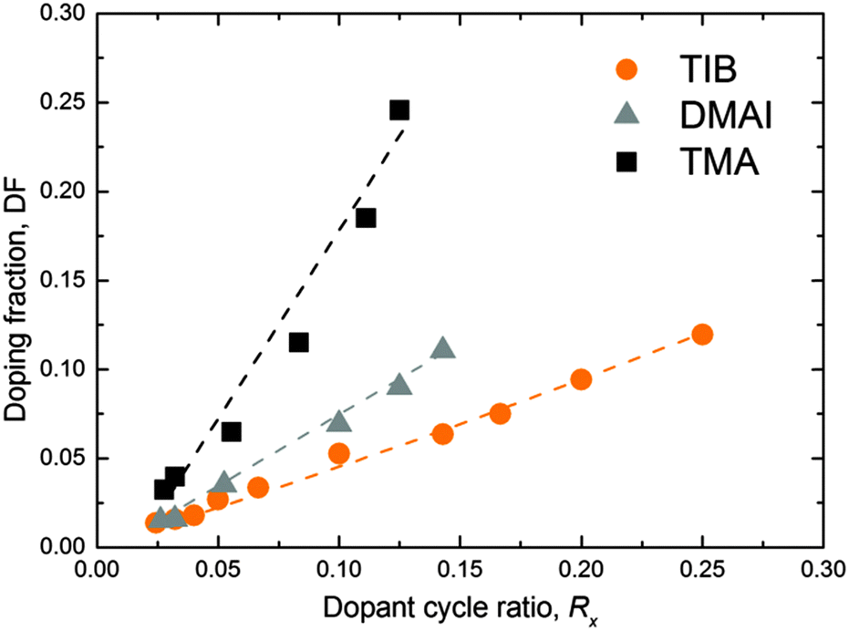 | ||
| Fig. 3 Doping fraction (DF) as a function of the doping cycle ratio Rx for depositions at 150 °C, as measured by X-ray photoelectron spectroscopy (XPS). The doping cycle ratio Rx (i.e. the ratio of the number of doping ALD cycles (X = Al, B) over the total ALD cycles in one supercycle) is calculated as 1/(m + 1). The estimated relative error for the doping fraction is ∼10%. The lines serve as guides to the eye. | ||
4.2. Electrical properties
The electrical properties of the 45 ± 5 nm-thick ZnO:B films deposited on glass substrates at a temperature of 150 °C are presented in Fig. 4. The addition of a small amount of B sharply reduced the resistivity of the films to a minimum of ∼3.5 mΩ cm for a DF of 0.016 (Fig. 4a). The films were benchmarked with ZnO:Al films of the same thickness and deposited at the same temperature using DMAI and TMA as Al precursors. The addition of Al also reduced the resistivity of the films to a minimum in both cases. Doping with DMAI resulted in ZnO:Al films with the same minimum resistivity than ZnO:B films at the same DF of 0.016, while doping with TMA resulted in ZnO:Al films with a higher minimum resistivity of 8 mΩ cm for a higher DF of 0.040. The resistivity of ZnO:Al films increased in both cases after achieving the minimum resistivity value, but this increase was more gradual than observed for the ZnO:B films.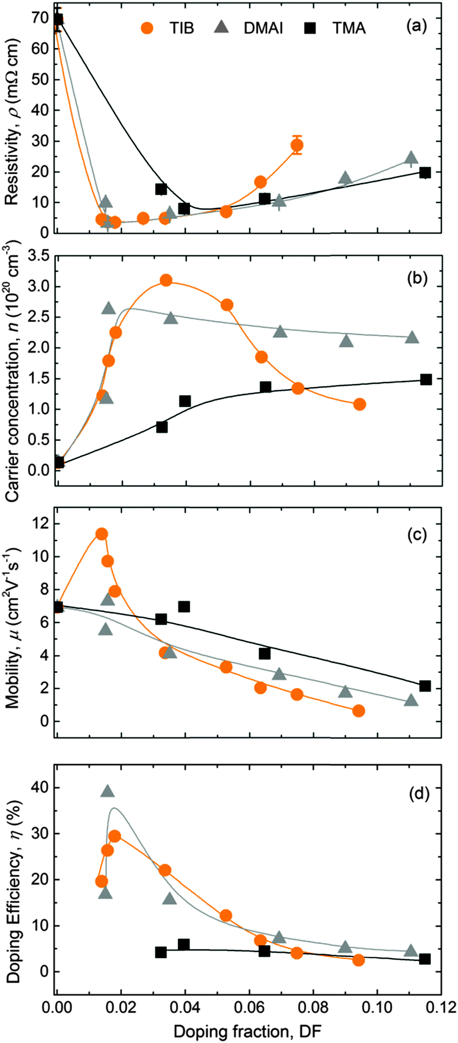 | ||
| Fig. 4 Resistivity, ρ (a), carrier concentration, n (b), mobility, μ (c) and doping efficiency η (d) of the ZnO:X (X = Al, B) films as a function of the doping fraction (DF) measured by XPS. TIB was used as a B source while DMAI and TMA were used as Al sources. All films had a thickness of 45 ± 5 nm and were deposited on glass substrates at 150 °C. The lines serve as guides to the eye. The error bars for ρ are plotted in the graph (some of them lying within the data points) and the estimated relative statistical uncertainties for n, μ and η are 3%, 5% and 20%, respectively. | ||
The carrier concentration extracted from the modelling of the SE data assuming an effective mass of 0.4 (Fig. 4b) was consistent with the carrier concentration obtained by Hall measurements (not shown). The carrier concentration increased with the addition of B until a maximum of 3.1 × 1020 cm−3 for a DF of 0.034 was achieved, after which the carrier concentration decreased abruptly. This trend is consistent with previous reports in the literature for ZnO:B layers deposited by chemical spray pyrolysis.126 In the case of ZnO:Al films doped with DMAI, the carrier concentration reached a maximum value of 2.6 × 1020 cm−3 for a DF of 0.016, before gradually decreasing to a value of ∼2.2 × 1020 cm−3 for higher doping fractions. For ZnO:Al films doped with TMA, the carrier concentration reached a maximum value of ∼1.4 × 1020 cm−3, which did not vary significantly at higher DF values than 0.06. Based on literature reports,60,68 it is expected that the carrier concentration will decrease abruptly for higher Al doping concentrations than those studied in this work. The increase of the carrier concentration for low doping fractions in the three cases can be assigned to the effective doping of B and Al, respectively (i.e., substitution of Zn2+ by B3+ or Al3+). The sharp decrease of the carrier concentration for TIB and the local saturation for DMAI and TMA might occur as a result of dopant occupying interstitial sites, dopant clustering, formation of oxides, or formation of metastable phases, making dopant inactive,60,126 which is possibly related to reaching the solubility limit of the B and Al into the ZnO lattice. For low doping fractions, the maximum mobility value for the ZnO:B films (i.e., 11.4 cm2 V−1 s−1) was 57% higher at low doping fractions relative to the maximum values determined for the ZnO:Al films. Based on the Masetti model for ionized impurity scattering,127,128 a mobility as high as 42 cm2 V−1 s−1 would be expected for the maximum carrier concentration of 3.1 × 1020 cm−3 in this work (ZnO:B film with DF = 0.034). Therefore, the overall lower values obtained for the three doping materials and the trend of mobility decreasing with increasing doping fraction over the full range studied (Fig. 4c) can most likely be attributed to grain boundary scattering.128 Furthermore, it is rather striking that μ increases when going from undoped ZnO to low B-doping concentrations, as one would expect more ionized impurity scattering. Yet a similar trend in mobility was observed for ZnO:B films prepared by the sol–gel technique.129
The doping efficiency (η), i.e., the ratio of the excess carrier density due to doping and the dopant density, is the percentage of dopant atoms that donate a free electron to the ZnO films and it is calculated using the equation
 | (1) |
In this equation, n and n0 are the carrier densities of doped (X = Al, B) and intrinsic ZnO films respectively; and NZn is the atomic density of Zn as measured by RBS (4.0 × 1022 cm−3).36 As can be seen in Fig. 4d, the alternative precursors, TIB and DMAI, showed the highest doping efficiency at low doping levels, i.e., 30–40% for a range of DF of 0.016–0.018 that resulted in the lowest resistivities for the ZnO:B and ZnO:Al (doped with DMAI) films.130 Both alternative precursors outperformed TMA in terms of doping efficiency, as a maximum doping efficiency of 6% was achieved using this conventional precursor. This is in line with previously reported results for ZnO:Al films doped with DMAI and TMA deposited at 250 °C.36
Compared to ZnO:Al films deposited at 250 °C, we found that processing at 150 °C led to lower absolute values of conductivity (i.e. a higher resistivity), carrier concentration, mobility and doping efficiency. For this reason, the effect of deposition temperature on the electrical properties of the ZnO:B films and the doping efficiency was investigated. ZnO:B films with thicknesses of 45 ± 5 nm were deposited at different temperatures (150–240 °C) using a cycle ratio with m = 24, which led to an optimised resistivity in the ZnO:B doping series shown in Fig. 4. The resistivity of the ZnO:B films decreased from 3.5 mΩ cm at 150 °C to 2.2 mΩ cm when deposited at temperatures of 200–240 °C. This was due to an increase in carrier concentration from 2.2 × 1020 cm−3 to 2.8 × 1020 cm−3 and an increase in mobility from 8 to 10.5 cm2 V−1 s−1. We would like to underline that the doping fraction increased with increasing deposition temperature, whereas the doping efficiency decreased slightly, despite the slight increase in carrier concentration with temperature. From Fig. 5, it can be concluded that ∼200 °C is the optimum deposition temperature for ZnO:B. However, it should be noted that the deposition temperature that is feasible for certain applications can be limited to lower temperatures than 200 °C. Furthermore, a brief study was conducted to assess the thickness dependence of the sheet resistance (Rs) for films up to 100–120 nm deposited at 200 °C (see Fig. S2 of the ESI†). A soft saturation on the Rs values was observed for thickness above ∼50 nm for the three doping precursors studied showing that a further increase in film thickness has a relatively minor impact on Rs.
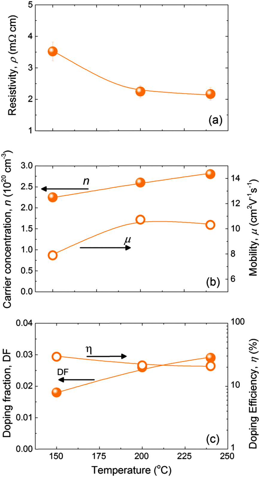 | ||
| Fig. 5 Resistivity, ρ (a), carrier concentration, n, and mobility, μ (b) and doping fraction, DF, and doping efficiency, η (c) of the ZnO:B films as a function of the deposition temperature. The films with thicknesses of 45 ± 5 nm were deposited on glass substrates. A cycle ratio of m = 24 was employed as it resulted in optimised resistivity in the doping series at 150 °C. The lines serve as guides to the eye. The estimated relative statistical uncertainties for n, μ, DF and η are 3%, 5%, 10% and 20%, respectively. | ||
4.3 Structural properties
The crystal structure of the ZnO:B films was characterized by XRD, and selected spectra are presented in Fig. 6. Similar patterns were observed for ZnO:Al doped using the DMAI precursor (see Fig. S3 of the ESI†). The intrinsic ZnO films were polycrystalline and exhibited an hexagonal wurtzite structure with a weak (002) texture (i.e., preferential growth orientation), consistent with what is reported in the literature.60,131 No peaks indicative of (crystalline) boron oxide phases were observed in the studied range of doping fractions. The intensity of the peaks decreased abruptly at a doping fraction of DF > 0.053 for ZnO:B films as expected for highly-doped ZnO films. Similar observations hold for the ZnO:Al films prepared with DMAI.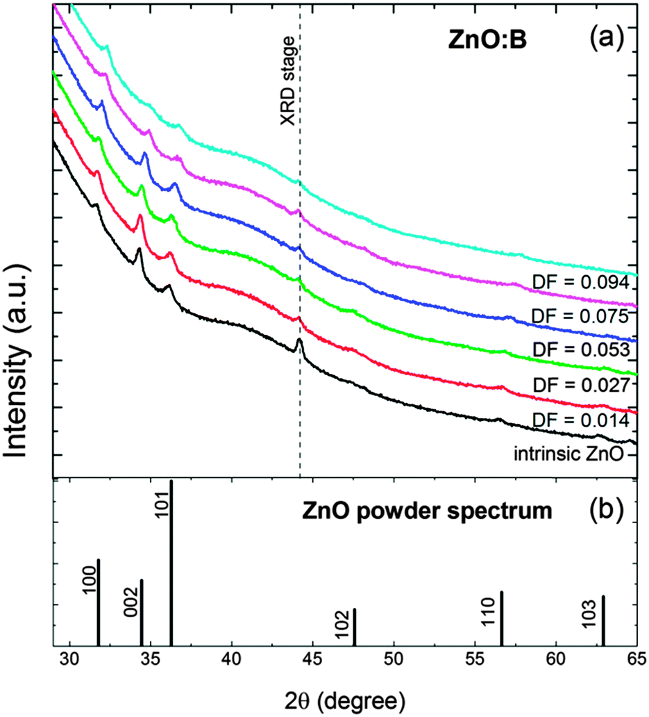 | ||
| Fig. 6 (a) XRD patterns of 45 nm-thick ZnO:B films deposited at 150 °C with different doping fractions (DF = 0.000–0.094) and (b) ZnO powder spectrum for reference. The peak labelled as ‘XRD stage’ corresponds to a peak related to the stage onto which the samples are mounted to perform the measurement, and its intensity is inversely proportional to the surface area of the sample. | ||
The XRD patterns of both the ZnO:B and ZnO:Al films revealed several interesting features. First of all, the intensity of the (002) peak decreased while that of the (100) peak increased for increasing doping fractions, indicating a change in texture of the ZnO:X films. This effect was more pronounced in the case of DMAI than in the case of TIB as shown in Fig. 7a. As a guide to the eye, the ratio I002/I100 for a powder pattern, i.e., the pattern characteristic for a film with randomly oriented crystals, has been included to illustrate the change in texture from 〈002〉 to 〈100〉. Secondly, a significant shift of the peaks to higher 2θ values was observed for increasing B fractions, which was likely due to compressive stress in the ZnO unit cell caused by the substitution of Zn2+ (ionic radius of 0.60 Å, assuming a four-coordinate environment as expected for wurtzite structures)132 with smaller B3+ ions (four-coordinate ionic radius of 0.11 Å).132 This effect was significantly smaller in the case of ZnO:Al films doped by DMAI (Al3+, four-coordinate ionic radius of 0.39 Å).132Fig. 7b shows the shift of the (002) peak as a function of the doping fraction, as a consequence of the compression of the unit cell (i.e. a decrease of the c-lattice parameter) with increasing doping fractions. It should be noticed that the c-lattice parameter for the pure ZnO films (i.e., DF = 0) was slightly larger (5.219 Å) than the value reported for the wurtzite ZnO crystal lattice (5.207 Å).6 This slight difference could be attributed to a combination of measurement inaccuracies (i.e., scan step size or a small sample misalignment in the z-direction), and sample conditions (i.e., stress in the film, or relatively small crystals).
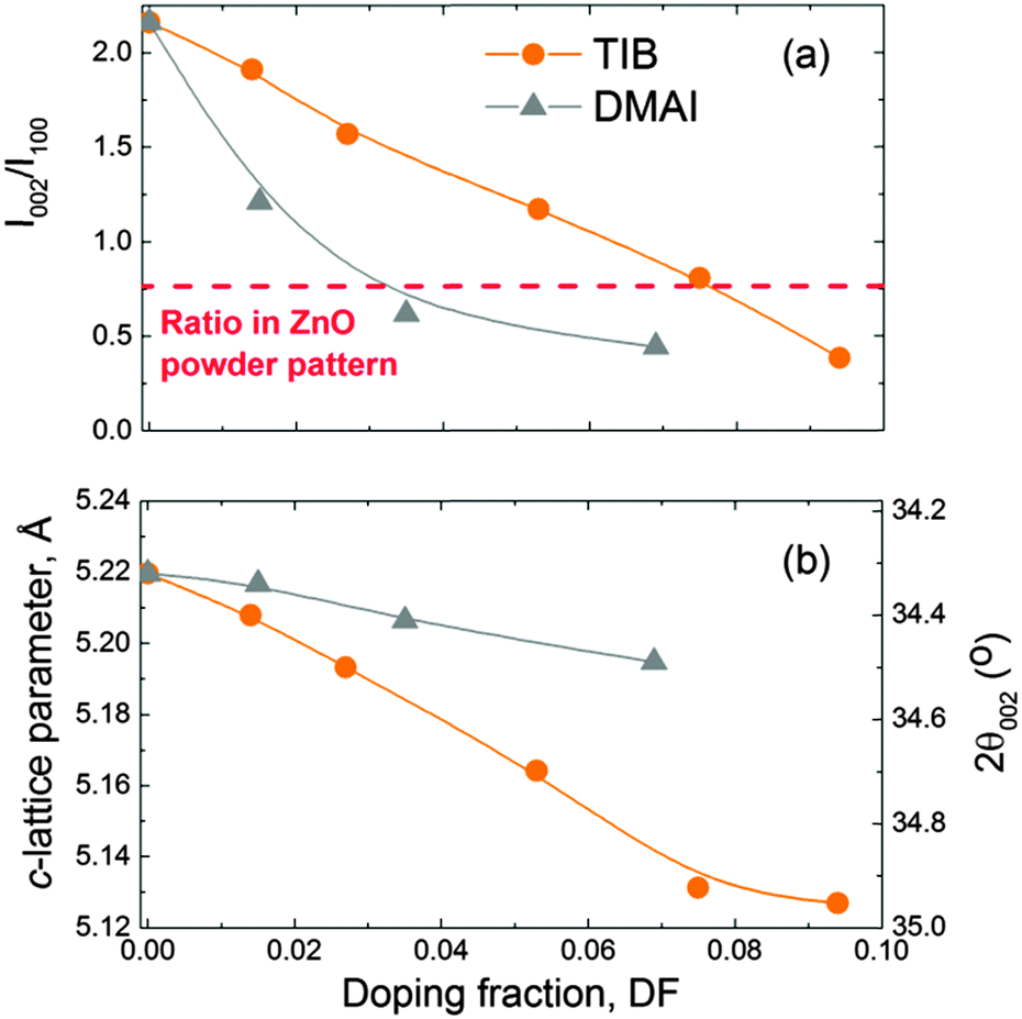 | ||
| Fig. 7 (a) Intensity ratio I002/I100 of the (002) and (100) peaks measured by XRD on the ZnO:X (X = Al, B) films reflecting the change in texture from 〈002〉 to 〈001〉 and (b) c-lattice parameter of the ZnO wurtzite unit cell and the corresponding 2θ position of the (002) peak as a function of the doping fraction in the ZnO:X (X = Al, B). The films were deposited at 150 °C on glass substrates. The c-lattice parameter of the wurtzite ZnO crystal is 5.207 Å.6 | ||
To further understand the nanostructure of the films, a TEM study was performed on two ZnO:B films with two different cycle ratios (m = 30 and 19) and a ZnO:Al (DMAI) film with m = 18 (Fig. 8). As visible in the bright field (BF) TEM images shown in Fig. 8a, both ZnO:B films were characterized by columnar grains stretching from the substrate to the surface, while the ZnO:Al film showed a somewhat interrupted grain growth, i.e., at several heights within the layer new crystals have nucleated and grown. The latter can most likely be attributed to the local presence of amorphous AlOx preventing epitaxial growth of ZnO on the underlying ZnO crystals after a DMAI cycle. In both ZnO:B films, it was difficult to distinguish the B-doped layers from the rest of the film, due to limited difference in average atomic number compared to the undoped ZnO. Only close to the interface with the substrate, these layers are vaguely discernible, as indicated by the arrows on the high-angle annular dark field (HAADF) STEM images in Fig. 8b. In contrast, the Al-doped layers were more clearly visible in the lower part of the ZnO:Al film than the ZnO:B films. The fact that the doped layers were only visible close to the interface to the substrate can be attributed to the surface roughness of the films, which increases as a function of vertical position in the layer due to the pyramid-shaped top facets of the growing ZnO crystals.
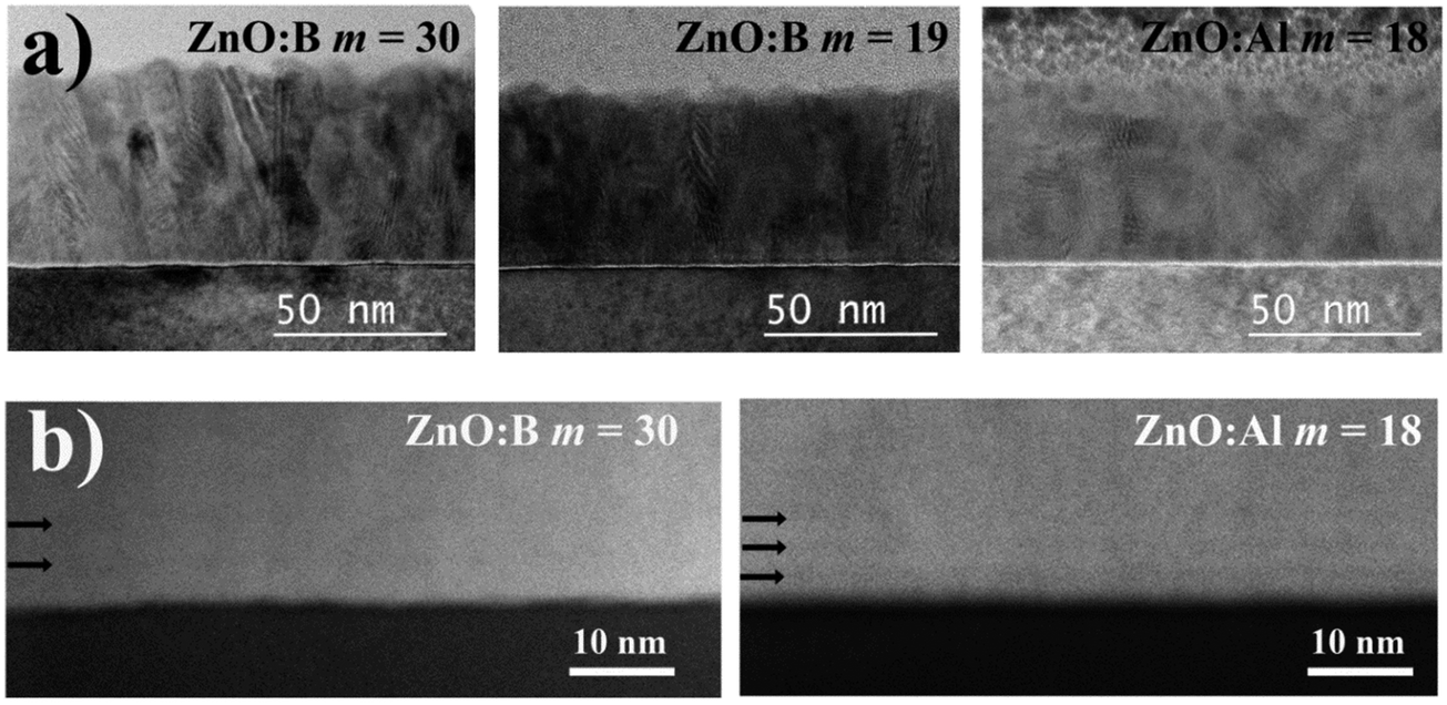 | ||
| Fig. 8 Transmission electron microscopy images: (a) bright-field (BF) TEM of two ZnO:B films (m = 30 and m = 19) and a ZnO:Al film (m = 18); and (b) high-angle annular dark field (HAADF) STEM images of ZnO:B (m = 30) and ZnO:Al (m = 18). The B- and Al-doped layers are indicated by arrows. | ||
4.4 Optical properties
The transmittance spectra of selected ZnO:B layers with different DF (0.000–0.063) are shown in Fig. 9. The transmittance values were over 90% in the major part of the visible and near-infrared (NIR) range. A decrease in transmittance was observed in the NIR region with increasing doping fraction until DF = 0.034. For higher DF values, the transmittance in the NIR increased again. This behaviour can be attributed to free-carrier absorption. Furthermore, a blue shift was observed in the ultraviolet absorption edge with increasing doping concentration from intrinsic ZnO to doped ZnO:B films with a DF of 0.063. This is due to the increase of the optical band gap. Both these aspects will be considered more in detail below.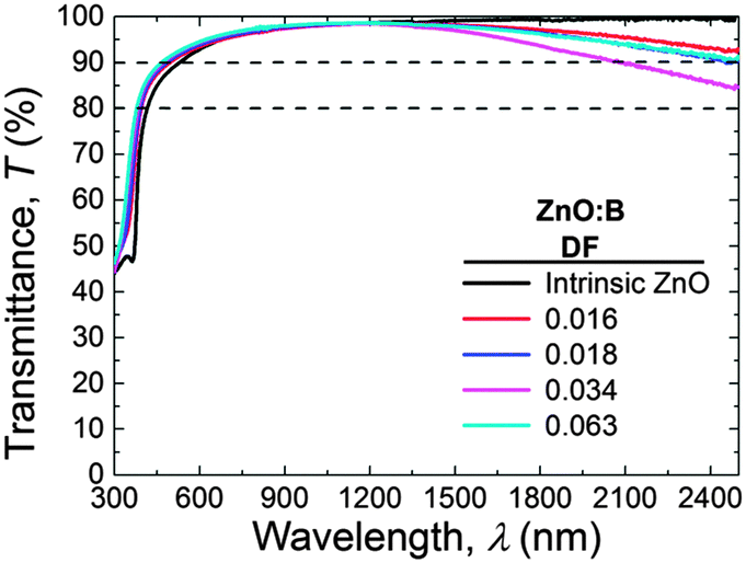 | ||
| Fig. 9 Transmittance of selected ZnO:B samples (DF = 0.000–0.063) deposited at 150 °C and with thicknesses of 45 ± 5 nm. | ||
The transmittance (T) of the ZnO:B films deposited on glass does not correct for interference effects in the films nor for the strong absorption peak of the glass substrates. Additionally, the transmittance is a film property and depends therefore on the film thickness. For these reasons, the ALD ZnO:B optical properties were assessed by studying the absorption coefficient (α) which was calculated from the SE data. Fig. 10 shows α as a function of the DF for ZnO:B films on a wide DF region (DF = 0.000–0.094). Clearly in the NIR region, the absorption decreases with increasing DF up to 0.034 whereas it increases again for higher DF values. This can be attributed to the free-carrier absorption in the films as described by the Drude model.133 The correlation of α with the free carrier density (n) is shown in the legend of the figure. The absorption coefficient of ZnO:Al films doped with DMAI follows a similar trend with n (see Fig. S4 for the absorption coefficient data of ZnO:Al using DMAI and TMA, ESI†).
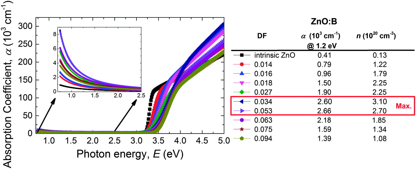 | ||
| Fig. 10 Absorption coefficient (α) as a function of the photon energy (E) of the ALD ZnO:B films deposited at 150 °C on glass substrates. | ||
The optical band gap (Eg,opt) of the ZnO:X films was extracted from so-called Tauc plots35,124 (i.e., (ε2E2)2 as a function of the photon energy E, where ε2 is the imaginary part of the dielectric function extracted from the SE data) as shown in Fig. S5 (ESI†). The optical band gap energies, calculated by linear fits to the data in the Tauc plots, are presented in Fig. 11 as a function of the DF. For ZnO:B, as well as for ZnO:Al, the optical band gap increases with increasing doping fraction. This increase can be attributed to the Burstein–Moss shift, but only for the range of DF values for which the carrier concentration n increases.60,68 For higher DF values (DF > 0.034), in the case of ZnO:B and ZnO:Al (DMAI), the increase in the optical bandgap can be attributed to effects related to the grain size,134 strain and other types of imperfections.135 Additionally, the fact that films start to have a considerable fraction of amorphous oxide with a higher bandgap than intrinsic ZnO plays probably a role. This holds especially for the case of Al-doping for which the formation of amorphous AlOx regions has become clear.35
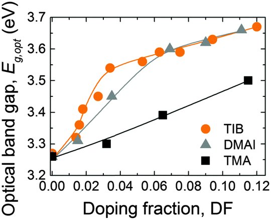 | ||
| Fig. 11 Optical band gap (Eg,opt) as a function of DF for ZnO:X (X = Al, B). TIB was used as a B source while DMAI and TMA were used as Al sources. The films were deposited on SiO2 substrates at 150 °C. | ||
5 Conclusions
Doped zinc oxide is a key transparent conducting oxide (TCO) material for many thin-film-based applications in optoelectronics. Atomic layer deposition (ALD) is a very promising technique to deposit high quality TCOs as doping materials can be introduced with greater control than with other deposition methods. Aluminium is by far the most common element to dope zinc oxide and especially trimethyl aluminium (TMA) is used as a precursor during ALD. The application of other dopants has been far less reported. For instance, B as a dopant has been scarcely reported for ALD probably due to the highly toxic nature of the traditional boron precursor diborane. We report here the feasibility of using a new, relatively safe boron precursor, triisopropyl borate (TIB), for the atomic layer deposition of ZnO:B. To benchmark the properties of the ZnO:B films, we also deposited ZnO:Al films using dimethylaluminium isopropoxide (DMAI) and TMA as alternative and conventional Al sources, respectively.Process wise, the use of the TIB precursor led to the better control over the doping (i.e. less dopant atoms per doping cycle are deposited) and to very high doping efficiencies, as compared to doping using TMA. The DMAI precursor resulted in similar high doping efficiencies (η ∼ 30–40%) to TIB. The conductivities and carrier concentrations of the films deposited using TIB and DMAI were significantly higher at lower doping fractions than that of ZnO:Al films where TMA was the aluminium source. The mobilities of ZnO:B films were significantly higher than those of the ZnO:Al films doped with DMAI and TMA at low doping fractions. Additionally, the transparency of the ZnO:B films was very high in most of the visible and near-infrared range. The excellent electrical and optical properties of selected ALD ZnO:B films deposited using TIB can be exploited to prepare, for instance, transparent conductive oxide films for silicon heterojunction solar cells for which the required thickness is ∼80 nm due to the fact that the film acts also as antireflection coating. The results showed that resistivities as low as 1.5 and 0.9 mΩ cm (i.e., sheet resistances Rs = 204 and 128 Ω sq−1) can be achieved for ∼80 nm-thick ZnO:B films deposited at temperatures of 150 °C and 200 °C, respectively. In both cases, transmittances higher than 80% for wavelengths >370 nm, but over 90% for wavelengths in the range 700–1750 nm can be achieved.
In light of these results, it is demonstrated that the use of novel alternative precursors for ALD can open new ways of doping ZnO more efficiently resulting in excellent electrical and optical film properties even at low temperatures.
Acknowledgements
The authors thank J. W. Weber, Dr H. C. M. Knoops and B. W. H. van de Loo (TU/e) for their invaluable input into the analysis of the SE data. We would also like to thank W. Keuning, B. Macco, and H. Gatz (TU/e) for their help with the XRD, AFM, and transmission measurements, respectively. This work was financially supported by the European Community’s 7th Framework Programme through the Marie Curie Intra-European Fellowship of D.G.-A. (ALD4PV, FP7-MC-IEF-272444) and by the Dutch Technology Foundation STW through the Flash Perspectief Programma. The research of W.M.M.K. has been made possible by the Dutch Technology Foundation STW and the Netherlands Organization for Scientific Research (NWO, VICI programme). Air Liquide is acknowledged for the donation of the DMAI and TIB precursors. Solliance, a solar energy R&D initiative of ECN, TNO, Holst, TU/e, imec and Forschungszentrum Jülich, and the Dutch province of Noord-Brabant are acknowledged for funding the TEM facility.Notes and references
- A. A. Rockett, Curr. Opin. Solid State Mater. Sci., 2010, 14, 143–148 CrossRef CAS.
- C. A. Wolden, J. Kurtin, J. B. Baxter, I. Repins, S. E. Shaheen, J. T. Torvik, A. A. Rockett, V. M. Fthenakis and E. S. Aydil, J. Vac. Sci. Technol., A, 2011, 29, 30801 Search PubMed.
- D. Song and B. Guo, J. Phys. D: Appl. Phys., 2009, 42, 25103 CrossRef.
- A. Janotti and C. G. Van de Walle, Rep. Prog. Phys., 2009, 72, 126501 CrossRef.
- C. Y. Chen, C. A. Lin, M. J. Chen, G. R. Lin and J. H. He, Nanotechnology, 2009, 20, 185605 CrossRef CAS PubMed.
- K. Ellmer and A. Klein, in Transparent Conductive Zinc Oxide: Basics and Applications in Thin Film Solar Cells, ed. K. Ellmer, A. Klein and B. Rech, Springer, Heidelberg, Germany, 2001, pp. 1–34 Search PubMed.
- F. Khan, Vandana, S. N. Singh, M. Husain and P. K. Singh, Sol. Energy Mater. Sol. Cells, 2012, 100, 57–60 CrossRef CAS.
- D.-J. Lee, H.-M. Kim, J.-Y. Kwon, H. Choi, S.-H. Kim and K.-B. Kim, Adv. Funct. Mater., 2011, 21, 448–455 CrossRef CAS.
- T. H. Breivik, S. Diplas, A. G. Ulyashin, A. E. Gunnæs, B. R. Olaisen, D. N. Wright, A. Holt and A. Olsen, Thin Solid Films, 2007, 515, 8479–8483 CrossRef CAS.
- L. Korte, E. Conrad, H. Angermann, R. Stangl and M. Schmidt, Sol. Energy Mater. Sol.Cells, 2009, 93, 905–910 CrossRef CAS.
- P. J. Rostan, U. Rau, V. X. Nguyen, T. Kirchartz, M. B. Schubert and J. H. Werner, Sol. Energy Mater. Sol. Cells, 2006, 90, 1345–1352 CrossRef CAS.
- M. Godlewski, E. Guziewicz, K. Kopalko, G. Łuka, M. I. Łukasiewicz, T. Krajewski, B. Witkowski and S. Gierałtowska, Low Temp. Phys., 2011, 37, 235–240 CrossRef CAS.
- M. Godlewski, E. Guziewicz, G. Łuka, T. Krajewski, M. Łukasiewicz, Ł. Wachnicki, A. Wachnicka, K. Kopalko, A. Sarem and B. Dalati, Thin Solid Films, 2009, 518, 1145–1148 CrossRef CAS.
- S. Park, S. J. Tark, J. S. Lee, H. Lim and D. Kim, Sol. Energy Mater. Sol. Cells, 2009, 93, 1020–1023 CrossRef CAS.
- A. Bauer, T. Wahl, J. Hanisch and E. Ahlswede, Appl. Phys. Lett., 2012, 100, 73307 CrossRef.
- M. K. Wu, T. Ling, Y. Xie, X. G. Huang and X. W. Du, Semicond. Sci. Technol., 2011, 26, 105001 CrossRef.
- G. Pérez-Hernández, A. Vega-Poot, I. Pérez-Juárez, J. M. Camacho, O. Arés, V. Rejón, J. L. Peña and G. Oskam, Sol. Energy Mater. Sol. Cells, 2012, 100, 21–26 CrossRef.
- W. Beyer, J. Hüpkes and H. Stiebig, Thin Solid Films, 2007, 516, 147–154 CrossRef CAS.
- D. K. Schroder, Semiconductor Material and Device Characterization, John Wiley & Sons, Hoboken, NJ, USA, 3rd edn, 2006 Search PubMed.
- M. Krunks and E. Mellikov, Thin Solid Films, 1995, 270, 33–36 CrossRef CAS.
- M. Gabás, N. T. Barrett, J. R. Ramos-Barrado, S. Gota, T. C. Rojas and M. C. López-Escalante, Sol. Energy Mater. Sol. Cells, 2009, 93, 1356–1365 CrossRef.
- A. Kyaw, X. Sun and C. Jiang, J. Sol-Gel Sci. Technol., 2009, 52, 348–355 CrossRef CAS.
- E. D. Spoerke, M. T. Lloyd, E. M. McCready, D. C. Olson, Y.-J. Lee and J. W. P. Hsu, Appl. Phys. Lett., 2009, 95, 213506 CrossRef.
- J. Herrero and C. Guillén, Thin Solid Films, 2004, 451–452, 630–633 CrossRef CAS.
- T. Minami, T. Mijata, K. Ihara, Y. Minamino and S. Tsukada, Thin Solid Films, 2006, 494, 47–52 CrossRef CAS.
- E. M. Kaidashev, M. Lorenz, H. von Wenckstern, A. Rahm, H.-C. Semmelhack, K.-H. Han, G. Benndorf, C. Bundesmann, H. Hochmuth and M. Grundmann, Appl. Phys. Lett., 2003, 82, 3901–3903 CrossRef CAS.
- A. Drici, G. Djeteli, G. Tchangbedji, H. Derouiche, K. Jondo, K. Napo, J. C. Bernède, S. Ouro-Djobo and M. Gbagba, Phys. Status Solidi A, 2004, 201, 1528–1536 CrossRef CAS.
- P. K. Nair, M. T. S. Nair, V. M. García, O. L. Arenas, Y. Peña, A. Castillo, I. T. Ayala, O. Gomezdaza, A. Sánchez, J. Campos, H. Hu, R. Suárez and M. E. Rincón, Sol. Energy Mater. Sol. Cells, 1998, 52, 313–344 CrossRef CAS.
- M. E. Fragalà, G. Malandrino, M. M. Giangregorio, M. Losurdo, G. Bruno, S. Lettieri, L. S. Amato and P. Maddalena, Chem. Vap. Deposition, 2009, 15, 327–333 Search PubMed.
- A. Hongsingthong, I. A. Yunaz, S. Miyajima and M. Konagai, Sol. Energy Mater. Sol. Cells, 2011, 95, 171–174 CrossRef CAS.
- A. Pourret, P. Guyot-Sionnest and J. W. Elam, Adv. Mater., 2009, 21, 232–235 CrossRef CAS.
- T. Tynell and M. Karppinen, Semicond. Sci. Technol., 2014, 29, 43001 CrossRef.
- J. R. Bakke, K. L. Pickrahn, T. P. Brennan and S. F. Bent, Nanoscale, 2011, 3, 3482–3508 RSC.
- J. A. van Delft, D. Garcia-Alonso and W. M. M. Kessels, Semicond. Sci. Technol., 2012, 27, 074002 CrossRef.
- Y. Wu, P. M. Hermkens, B. W. H. van de Loo, H. C. M. Knoops, S. E. Potts, M. A. Verheijen, F. Roozeboom and W. M. M. Kessels, J. Appl. Phys., 2013, 114, 24308 CrossRef.
- Y. Wu, S. E. Potts, P. M. Hermkens, H. C. M. Knoops, F. Roozeboom and W. M. M. Kessels, Chem. Mater., 2013, 25, 4619–4622 CrossRef CAS.
- M. Leskelä and M. Ritala, Thin Solid Films, 2002, 409, 138–146 CrossRef.
- S. M. George, Chem. Rev., 2010, 110, 111–131 CrossRef CAS PubMed.
- S. E. Potts, H. B. Profijt, R. Roelofs and W. M. M. Kessels, Chem. Vap. Deposition, 2013, 19, 125–133 CrossRef CAS.
- S. E. Potts and W. M. M. Kessels, Coord. Chem. Rev., 2013, 257, 3254–3270 CrossRef CAS.
- S. E. Potts, W. Keuning, E. Langereis, G. Dingemans, M. C. M. van de Sanden and W. M. M. Kessels, J. Electrochem. Soc., 2010, 157, P66–P74 CrossRef CAS.
- A. Devi, Coord. Chem. Rev., 2013, 257, 3332–3384 CrossRef CAS.
- J. W. Elam, Z. A. Sechrist and S. M. George, Thin Solid Films, 2002, 414, 43–55 CrossRef CAS.
- A. Abou Chaaya, R. Viter, I. Baleviciute, M. Bechelany, A. Ramanavivius, Z. Gertnere, D. Erts, V. Smyntyna and P. Miele, J. Phys. Chem. C, 2014, 118, 3811–3819 Search PubMed.
- W. F. A. Besling, E. Young, T. Conard, C. Zhao, R. Carter, W. Vandervorst, M. Caymax, S. De Gendt, M. Heyns, J. Maes, M. Tuominen and S. Haukka, J. Non-Cryst. Solids, 2002, 303, 123–133 CrossRef CAS.
- D. R. G. Mitchell, G. Triani, D. J. Attard, K. S. Finnie, P. J. Evans, C. J. Barbé and J. R. Bartlett, Smart Mater. Struct., 2006, 15, S57–S64 CrossRef CAS.
- S. W. Smith, K. G. McAuliffe and J. F. Conley, Solid-State Electron., 2010, 54, 1076–1082 CrossRef CAS.
- V. Lujala, J. Skarp, M. Tammenmaa and T. Suntola, Appl. Surf. Sci., 1994, 82–83, 34–40 CrossRef.
- M. Čeh, H.-C. Chen, M.-J. Chen, J.-R. Yang and M. Shiojiri, Mater. Trans., JIM, 2010, 51, 219–226 CrossRef.
- N. P. Dasgupta, S. Neubert, W. Lee, O. Trejo, J.-R. Lee and F. B. Prinz, Chem. Mater., 2010, 22, 4769–4775 CrossRef CAS.
- D.-J. Lee, J.-Y. Kwon, S.-H. Kim, H.-M. Kim and K.-B. Kim, J. Electrochem. Soc., 2011, 158, D277–D281 CrossRef CAS.
- Y. Geng, Z.-Y. Xie, S.-S. Xu, Q.-Q. Sun, S.-J. Ding, H.-L. Lu and D. W. Zhang, ECS J. Solid State Sci. Technol., 2012, 1, N45–N48 CrossRef CAS.
- Z. Baji, Z. Lábadi, Z. E. Horváth and I. Bársony, Thin Solid Films, 2012, 5201, 4703–4706 CrossRef.
- P. Genevée, F. Donsanti, G. Renou and D. Lincot, Appl. Surf. Sci., 2013, 264, 464–469 CrossRef.
- A. Frölich and M. Wegener, Opt. Mater. Express, 2011, 1, 883–889 CrossRef.
- G. Luka, L. Wachnicki, B. S. Witkowski, T. A. Krajewski, R. Jakiena, E. Guziewicz and M. Godlewski, Mater. Sci. Eng., B, 2011, 176, 237–241 CrossRef CAS.
- G. Luka, T. A. Krajewski, B. S. Witkowski, G. Wisz, I. S. Virt, E. Guziewicz and M. Godlewski, J. Mater. Sci., 2011, 22, 1810–1815 CAS.
- Y.-C. Cheng, Appl. Surf. Sci., 2011, 258, 604–607 CrossRef CAS.
- T. Dhakal, D. Vanhart, R. Christian, A. Nandur, A. Sharma and C. R. Westgate, J. Vac. Sci. Technol., A, 2012, 30, 021202 Search PubMed.
- P. Banerjee, W.-J. Lee, K.-R. Bae, S. B. Lee and G. W. Rubloff, J. Appl. Phys., 2010, 108, 43504 CrossRef.
- S. J. Kwon, Jpn. J. Appl. Phys., 2005, 44, 1062–1066 CrossRef CAS.
- W. J. Maeng, J.-W. Lee, J. H. Lee, K.-B. Chung and J.-S. Park, J. Phys. D: Appl. Phys., 2011, 44, 445305 CrossRef.
- W. J. Maeng, S.-J. Kim, J.-S. Park, K.-B. Chung and H. Kim, J. Vac. Sci. Technol., B: Nanotechnol. Microelectron.: Mater., Process., Meas., Phenom., 2012, 30, 31210 CrossRef.
- Q. Hou, F. Meng and J. Sun, Nanoscale Res. Lett., 2013, 8, 144 CrossRef PubMed.
- R. M. Mundle, H. S. Terry, K. Santiago, D. Shaw, M. Bahoura, A. K. Pradhan, K. Dasari and R. Palai, J. Vac. Sci. Technol., A, 2013, 31, 01A146 Search PubMed.
- T. Tynell, R. Okazaki, I. Terasaki, H. Yamauchi and M. Karppinen, J. Mater. Sci., 2013, 48, 2806–2811 CrossRef CAS.
- T. Tynell, H. Yamauchi, M. Karppinen, R. Okazaki and I. Terasaki, J. Vac. Sci. Technol., A, 2013, 31, 01A109 Search PubMed.
- C. H. Ahn, H. Kim and H. K. Cho, Thin Solid Films, 2010, 519, 747–750 CrossRef CAS.
- J. W. Elam and S. M. George, Chem. Mater., 2003, 15, 1020–1028 CrossRef CAS.
- J. W. Elam, D. Routkevitch and S. M. George, J. Electrochem. Soc., 2003, 150, G339–G347 CrossRef CAS.
- J.-S. Na, Q. Peng, G. Scarel and G. N. Parsons, Chem. Mater., 2009, 21, 5585–5593 CrossRef CAS.
- J.-S. Na, G. Scarel and G. N. Parsons, J. Phys. Chem., 2010, 114, 383–388 CAS.
- O. Bethge, M. Nobile, S. Abermann, M. Glaser and E. Bertagnolli, Sol. Energy Mater. Sol. Cells, 2013, 117, 178–182 CrossRef CAS.
- L. Karvonen, A. Säynätjoki, Y. Chen, H. Jussila, J. Rönn, M. Ruoho, T. Alasaarela, S. Kujala, R. A. Norwood, N. Peyghambarian, K. Kieu and S. Honkanen, Appl. Phys. Lett., 2013, 103, 31903 CrossRef.
- Y. J. Choi, B. Gong, C.-S. Park, H.-S. Lee, J. G. Jang, H. J. Chang, G. Y. Yeom and H.-H. Park, ACS Appl. Mater. Interfaces, 2013, 5, 3650–3655 CAS.
- A. Illiberi, R. Scherpenborg, Y. Wu, F. Roozeboom and P. Poodt, ACS Appl. Mater. Interfaces, 2013, 5, 13124–13128 CAS.
- H. Yuan, B. Luo, D. Yu, A.-J. Cheng, S. A. Campbell and W. L. Gladfelter, J. Vac. Sci. Technol., A, 2012, 30, 01A138 Search PubMed.
- W. M. Haynes, CRC Handbook of Chemistry and Physics, CRC, Boca Raton, 93rd edn, 2012 Search PubMed.
- X. Qian, Y. Cao, B. Guo, H. Zhai and A. Li, Chem. Vap. Deposition, 2013, 19, 180–185 CrossRef CAS.
- W. Fieggen, H. Gerding and N. M. M. Nibbering, Recl. Trav. Chim. Pays-Bas, 1968, 87, 377–383 CrossRef CAS.
- J. Koo, S. K. Kim, S. Joen, H. Jeon, Y. Kim and Y. Won, J. Korean Phys. Soc., 2006, 48, 131–136 CAS.
- S. E. Potts, G. Dingemans, C. Lachaud and W. M. M. Kessels, J. Vac. Sci. Technol., A, 2012, 30, 21505 Search PubMed.
- C. R. Ellinger and S. F. Nelson, Chem. Mater., 2014, 26, 1514–1522 CrossRef CAS.
- K.-S. An, W. Cho, B. K. Lee, S. S. Lee and C. G. Kim, J. Nanosci. Nanotechnol., 2008, 8, 4856–4859 CrossRef CAS PubMed.
- B. Sang, A. Yamada and M. Konagai, Jpn. J. Appl. Phys., 1998, 37, 206–208 Search PubMed.
- A. Yamada, B. Sang and M. Konagai, Appl. Surf. Sci., 1997, 112, 216–222 CrossRef CAS.
- Y. Yamamoto, K. Saito, K. Takahashi and M. Konagai, Sol. Energy Mater. Sol. Cells, 2001, 65, 125–132 CrossRef CAS.
- B. Sang, A. Yamada and M. Konagai, Sol. Energy Mater. Sol. Cells, 1997, 49, 19–26 CrossRef CAS.
- Sigma-Aldrich, MSDS Diborane, No. 463051.
- S. Faÿ, U. Kroll, C. Bucher, E. Vallat-Sauvain and A. Shah, Sol. Energy Mater. Sol. Cells, 2005, 86, 385–397 CrossRef.
- X. L. Chen, X. H. Geng, J. M. Xue, D. K. Zhang, G. F. Hou and Y. Zhao, J. Cryst. Growth, 2006, 296, 43–50 CrossRef CAS.
- C. Yan, X. Chen, F. H. Wang, J. Sun, D. Zhang, C. Wei, X. Zhang, Y. Zhao and X. Geng, Thin Solid Films, 2012, 521, 249–252 CrossRef CAS.
- J. Yin, H. Zhu, Y. Wang, Z. Wang, J. Gao, Y. Mai, Y. Ma, M. Wan and Y. Huang, Appl. Surf. Sci., 2012, 259, 758–763 CrossRef CAS.
- I.-H. Choi, J. Korean Phys. Soc., 2013, 63, 1997–2001 CrossRef CAS.
- J.-C. Hsiao, C.-H. Chen, H.-J. Yang, C.-L. Wu, C.-M. Fan, C.-F. Huang, C.-C. Lin, P. Yu and J.-C. Hwang, J. Taiwan Inst. Chem. Eng., 2013, 44, 758–761 CrossRef CAS.
- Z. Hu, J. Zhang and Y. Zhu, Sol. Energy Mater. Sol. Cells, 2013, 117, 610–616 CrossRef CAS.
- J.-W. Schüttauf, G. Bugnon, M. Stuckelberger, S. Hanni, M. Boccard, M. Despeisse, F.-J. Haug, F. Meillaud and C. Ballif, IEEE Journal of Photovoltaics, 2014, 4, 757–762 CrossRef.
- M. L. Addonizio and A. Antonaia, J. Mater. Chem. C, 2013, 117, 24268–24276 CAS.
- D. R. Lide and H. V Kehiaian, CRC Handbook of Thermophysical and Thermochemical Data, CRC Press, Boca Raton, FL, 1994 Search PubMed.
- J.-S. Li, C.-R. Zhang, B.-Z. Li, F. Cao and S.-Q. Wang, Surf. Coat. Technol., 2011, 205, 3736–3741 CrossRef CAS.
- H. Wu, M. Chen, X. Wei, M. Ge and W. Zhang, Appl. Surf. Sci., 2010, 257, 1276–1281 CrossRef CAS.
- W. Kalss, R. Haubner and B. Lux, Int. J. Refract. Met. Hard Mater., 1998, 16, 233–241 CrossRef CAS.
- R. Weissenbacher and R. Haubner, Int. J. Refract. Met. Hard Mater., 2002, 20, 135–141 CrossRef CAS.
- C. Lorrette, P. Weisbecker, S. Jacques, R. Pailler and J. M. Goyhénèche, J. Eur. Ceram. Soc., 2007, 27, 2737–2743 CrossRef CAS.
- M. A. Mannan, H. Noguchi, T. Kida, M. Nagano, N. Hirao and Y. Baba, Thin Solid Films, 2010, 518, 4163–4169 CrossRef.
- M. A. Mannan, Y. Baba, T. Kida, M. Nagano, I. Shomoyama, N. Hirao and H. Noguchi, Thin Solid Films, 2011, 519, 1780–1786 CrossRef CAS.
- M. Putkonen and L. Niinistö, Thin Solid Films, 2006, 514, 145–149 CrossRef CAS.
- J. Olander, L. M. Ottosson, P. Heszler, J.-O. Carlsson and K. M. E. Larsson, Chem. Vap. Deposition, 2005, 11, 330–337 CrossRef CAS.
- D. Jahan and A. Pinchart, Proc. 25th Eur. Photovolt. Sol. Energy Conf., 2010, pp. 2919–2923 Search PubMed.
- C. Lachaud, A. Madec, A. Pinchart, S. Nicolay, J. P. Escarre and C. Ballif, Proc. 26th Eur. Photovolt. Sol. Energy Conf., 2011, pp. 2658–2662 Search PubMed.
- W. M. M. Kessels and M. Putkonen, MRS Bull., 2011, 36, 907–913 CrossRef CAS.
- Sigma-Aldrich, MSDS Diethylzinc, No. 668729.
- Sigma-Aldrich, MSDS Triisopropyl Borate, No. 197335.
- Sigma-Aldrich, MSDS Trimethylaluminum, No. 597775.
- Sigma-Aldrich, MSDS Dimethylaluminum Isopropoxide, No. J100047.
- H. Dumont, A. Marbeuf, J. Bourée and O. Gorochov, J. Mater. Chem., 1992, 2, 923–930 RSC.
- H. Dumont, A. Marbeuf, J.-E. Bourée and O. Gorochov, J. Mater. Chem., 1993, 3, 1075–1079 RSC.
- M. Söderlund, P. Mäke-Arvela, K. Eränen, T. Salmi, R. Rahkola and D. M. Murzin, Catal. Lett., 2005, 105, 191–202 CrossRef.
- D. W. Squire, C. S. Dulcey and M. C. Lin, J. Vac. Sci. Technol., B: Microelectron. Process. Phenom., 1985, 3, 1513–1519 CAS.
- S. Y. Lee, B. Luo, Y. Sun, J. M. White and Y. Kim, Appl. Surf. Sci., 2004, 222, 234–242 CrossRef CAS.
- M. Fulem, K. Růžička, V. Růžička, E. Hulicius, T. Šimeček, K. Melichar, J. Pangrác, S. A. Rushworth and L. M. Smith, J. Cryst. Growth, 2003, 248, 99–107 CrossRef CAS.
- S. S. Lee, E.-S. Lee, S. H. Kim, B. K. Lee, S. J. Jeong, J. H. Hwang, C. G. Kim, T.-M. Chung and K.-S. An, Bull. Korean Chem. Soc., 2012, 33, 2207–2212 CrossRef CAS.
- E. Langereis, S. B. S. Heil, H. C. M. Knoops, W. Keuning, M. C. M. van de Sanden and W. M. M. Kessels, J. Phys. D: Appl. Phys., 2009, 42, 73001 CrossRef.
- J. Tauc, R. Grigorovici and A. Vancu, Phys. Status Solidi B, 1966, 15, 627–637 CrossRef CAS.
- R. L. Puurunen, Appl. Surf. Sci., 2005, 245, 6–10 CrossRef CAS.
- B. N. Pawar, S. R. Jadkar and M. G. Takwale, J. Phys. Chem. Solids, 2005, 66, 1779–1782 CrossRef CAS.
- G. Masetti, M. Severi and S. Solmi, IEEE Trans. Electron Devices, 1983, 30, 764–769 CrossRef.
- K. Ellmer and R. Mientus, Thin Solid Films, 2008, 516, 4620–4627 CrossRef CAS.
- R. B. H. Tahar and N. B. H. Tahar, J. Mater. Sci., 2005, 40, 5285–5289 CrossRef CAS.
- Because DF is in the denominator in eqn (1), the doping efficiency is extremely sensitive to DF and therefore, the absolute values presented in Fig. 4d should not be over-interpreted, especially for low doping concentrations for which the error in DF is relatively large.
- V. Khranovskyy, U. Grossner, O. Nilsen, V. Lazorenko, G. V. Lashkarev, B. G. Svensson and R. Yakimova, Thin Solid Films, 2006, 515, 472–476 CrossRef CAS.
- R. D. Shannon, Acta Crystallogr., Sect. A: Cryst. Phys., Diffr., Theor. Gen. Crystallogr., 1976, 32, 751–767 CrossRef.
- V. Kumar, R. G. Singh, L. P. Purohit and R. M. Mehra, J. Mater. Sci. Technol., 2011, 27, 481–488 CAS.
- X. M. Lu, J. S. Zhu, W. Y. Zhang, G. Q. Ma and Y. N. Wang, Thin Solid Films, 1996, 274, 165–168 CrossRef CAS.
- B. Sernelius, K.-F. Berggren, Z.-C. Jin, I. Hamberg and C. Granqvist, Phys. Rev. B: Condens. Matter Mater. Phys., 1988, 37, 10244–10248 CrossRef CAS.
Footnote |
| † Electronic supplementary information (ESI) available. See DOI: 10.1039/c4tc02707h |
| This journal is © The Royal Society of Chemistry 2015 |