
 Open Access Article
 This Open Access Article is licensed under a
 Creative Commons Attribution 3.0 Unported Licence
Inkjet printed paper based frequency selective surfaces and skin mounted RFID tags: the interrelation between silver nanoparticle ink, paper substrate and low temperature sintering technique†
Veronica
Sanchez-Romaguera
*a,
Sebastian
Wünscher
bc,
Badredin M.
Turki
d,
Robert
Abbel
e,
Silvia
Barbosa
f,
Daniel J.
Tate
a,
Dumtoochukwu
Oyeka
d,
John C.
Batchelor
d,
Edward A.
Parker
d,
Ulrich S.
Schubert
bc and
Stephen G.
Yeates
*a
aOrganic Materials Innovation Centre (OMIC), School of Chemistry, The University of Manchester, M13 9PL, Manchester, UK. E-mail: veronica.sanchezromaguera@mbs.ac.uk; stephen.yeates@manchester.ac.uk
bLaboratory of Organic and Macromolecular Chemistry (IOMC), Friedrich Schiller University Jena, Humboldtstr. 10, 07743 Jena, Germany
cJena Center for Soft Matter (JCSM), Friedrich Schiller University Jena, Philosophenweg 7, 07743 Jena, Germany
dSchool of Engineering and Digital Art, University of Kent, CT2 7NT, Kent, United Kingdom
eHolst Centre-TNO, High Tech Campus 31, 5656 AE Eindhoven, The Netherlands
fCondensed Matter Physics Department, Faculty of Physics, Universidade de Santiago de, Compostela, 15782 Santiago de Compostela, Spain
First published on 6th January 2015
Abstract
Inkjet printing of functional frequency selective surfaces (FSS) and radio frequency identification (RFID) tags on commercial paper substrates using silver nanoparticle inks sintered using low temperature thermal, plasma and photonic techniques is reported. Printed and sintered FSS devices demonstrate performances which achieve wireless communication requirements having a forward transmission scattering parameter, S21, depth greater than −20 dB at 13 GHz. Printed and plasma sintered RFID tags on transfer paper, which are capable of being mounted on skin, improved read distances compared to previously reported single layer transfer RFID tags fabricated by conventional thermal sintering.
1. Introduction
With an increasing dependence on wireless communication, the demand for the integration of electronic structures onto a broader range of substrates is becoming increasingly important. In this paper, we consider two such wireless structures, both of which have the unified requirement of having the need to print conductive features onto substrates which will not tolerate high processing temperatures and how consideration of the interplay between ink and paper substrate coupled with selection of the appropriate sintering techniques is essential in realizing optimum performance.Firstly frequency selective surfaces (FSS) can be regarded as filters of electromagnetic waves and whilst well known in micro- and millimeter-wave aerospace systems, recent applications in ultra-high frequency (UHF) mobile bands have given rise to new design and fabrication requirements, including large physical size and low-cost manufacture.1,2 Current mobile and wireless systems are becoming severely capacity limited owing to interference and frequency reuse issues.3 A possible means to address the problem is to embed potentially large FSS panels within building structures such as FSS-wall paper, FSS-blinds, FSS-curtains and FSS-removable window covers. To be a realistic proposition, these panels must be simple to fabricate, low-cost and compatible with a wider range of materials, including temperature sensitive substrates.4 Aiming to address this gap, we recently reported the first digitally fabricated FSS on a temperature sensitive foil, polyethylene napthenate (PEN), which showed the potential of inkjet printing for the fabrication of FSS of similar performance to those fabricated with conventional etching techniques.5 Subsequent inkjet printed FSS reports have demonstrated both pre-coated textile and porous paper substrates6 have necessitated multiple layer deposition (up to 10 layers) in combination with long sintering times (>60 min) and high sintering temperature (160 °C) in order to obtain sufficiently conductive features.7
Secondly passive radio frequency identification (RFID) tags which are used in both asset management and in monitoring, identifying and tracking people particularly in work environments such as power plants, airports, hospitals, military bases, refineries and access restricted areas is an emerging application area. Recently, we reported the inkjet fabrication of UHF RFID tags, which were transferable onto skin. Commercially available non-porous transfer tattoo paper, silver nanoparticle ink, and moderate temperature conventional thermal sintering (135 °C, 30 min) were used to produce the UHF RFID tags.8 Although the potential of inkjet printing to obtain paper based electromagnetic structures such as FSS and UHF RFID has been demonstrated, the need for conventional thermal sintering techniques to convert the silver ink into suitably conductive features is still a limiting factor for applications on more thermally sensitive substrates and for roll-to-roll (R2R) manufacturing.
Alternative approaches to thermal sintering of silver nanoparticles have recently been reported enhancing the compatibility of the sintering step with thermally sensitive substrates and with R2R manufacturing capabilities.9 These have included tailoring the inks such that they can be processed at low temperatures,10 the use of sintering additives,11,12 application of an electrical current,13 exposure to low- and atmospheric-pressure plasmas,14,15 microwave irradiation16 and several photonic approaches including infra-red (IR),17 laser18 and intense pulsed light (IPL) sintering.19,20
Although some authors have reported sintering of silver nanoparticles on paper substrates21–24 and others have conducted feasibility studies on plastic substrates to compare the sintering effectiveness of various alternative low-temperature sintering techniques,25 to the best of our knowledge, no comparative study on the interrelation between different silver nanoparticle inks, paper substrates and various alternative sintering methods in addition to conventional thermal sintering has been reported. This work provides a systematic study of the electrical performance of inkjet printed features by comparing two commercially available inks, two commercially available paper substrates and three low-temperature sintering techniques, thermal, low-pressure argon plasma and IPL with a focus on FSS and tattoo RFID applications. Conclusions are drawn with regards to combinations of ink-paper substrate-printing and sintering techniques with potential for R2R manufacturing and commercial viability.
2. Experimental section
2.1 Materials
Two commercial silver nanoparticle dispersions were used in this work. Ink A is a 20 wt% dispersion of silver nanoparticles, (particle diameter in the range of 50 nm by scanning electron microscopy (SEM)) in ethanol/ethylene glycol mixture from Sigma-Aldrich (SunTronic U5603 from Sun Chemicals). Ink B is a water-based dispersion from Clearjet Ltd. (Jerusalem, Israel) containing 30 wt% of silver nanoparticles having a diameter of 10 nm. A detailed investigation of the composition of this ink can be found in a previously reported study.26Two paper substrates engineered for inkjet printing were chosen. Inkjet tattoo transfer paper (tattoo paper), representative of the paper class having a polymeric receiving layer, was supplied by Crafty Computer Paper (Leicester, UK) whilst PEL Nano-P60 paper (PEL paper), representative of the paper class having an inorganic micro-porous receiving layer, was obtained from Printed Electronics Ltd. (Cambridge, UK). In all cases the substrates were purged with a flow of air to remove dust particles prior to use.
2.2 Inkjet printing and sintering
Inkjet printing was performed using a piezoelectric Dimatix DMP-2800 system (Dimatix-Fujifilm Inc., USA), equipped with a 10 pL cartridge (DMC-11610). The cartridge temperature was set between 30 and 45 °C and was adapted to the applied substrate temperature.Thermal sintering was carried out in a convection oven set at 150 °C unless otherwise stated. Sintering times of up to 60 min were used as stated in the main text. Plasma sintering was performed using a low-pressure argon plasma instrument from Diener Electronic (Nagold, Germany). Small samples were processed with the Diener pico plasma chamber operating at a power of 190 W and a processing pressure of 0.4 mbar. Large area samples (A4 FSS) were processed with the Diener nano plasma chamber operating at a power of 300 W and a pressure of 0.4 mbar. Photonic flash sintering was carried out with a custom tool previously described.27,28 It consists of a combination of a XOP-15 lamp in an elliptical reflector and a commercially available flash lamp system (Sinteron 2000 from Xenon Corp., U.S.A.) mounted above a substrate holder which can be transported underneath the lamps at a predefined speed up to 20 m min−1.
2.3 Characterization
Thermogravimetric analysis (TGA) was performed under ambient atmosphere in the range from room temperature to 600 °C at a heating rate of 10 °C min−1 using a TGAQ5000 system from TA Instruments (NewCastle, USA). The electrical resistance of sintered silver features was measured by the 4-point probe technique. A Jandel multi-position wafer probe system (Jandel Engineering Ltd., Leighton Buzzard, UK) mounted with a cylindrical probe head (solid tungsten carbide needles of 0.40 mm diameter spaced 1.0 mm) was employed. Grazing angle FT-IR experiments were performed on a Vertex-70 spectrometer equipped with a Harrick Seagull accessory and Germanium hemisphere ATR crystal and nitrogen purge from Bruker. The sample was mounted with an incident angle of 65°. Background and measurements were averaged over 64 scans with a resolution of 4 cm−1, recorded by a DLaTGS detector.Optical microscopy images were taken using a Leica® DM25000 M optical microscope with adjustable magnification in reflective mode. Scanning electron microscopy (SEM) images were taken using an EVO® LS 15 system (Carl Zeiss AG, Oberkochen, Germany) operating at an accelerating voltage of 20 kV.
The FSS design used in this work has been described in our earlier work30 consisting of 374 patch dipoles set on a skewed lattice (Fig. S7†). The RFID antenna used in this work has a total size of 65 × 20 mm2 including a port area, and is described in detail in our previous study (Fig. S7†).9 Tag read distance was measured using a Voyantic Tagformance lite RFID measurement system. After calibrating the system at 35 cm the RFID tag was transferred to the volunteers arm and the read range was extrapolated by measurement at the global RFID UHF frequency bands within permitted transmission power levels.
3. Results and discussion
3.1 Characterization of paper substrates
The papers used in this study are representative of the two major classes of commercial inkjet paper, polymer coated and inorganic micro-porous. The composition and thermal stability of polymer coated tattoo transfer paper has previously been described and comprises a 1 μm thick non-porous ink-receiving layer primarily composed of polyvinyl alcohol (PVA) which limits the sintering temperature to 135 °C (Fig. S1a–c†).8 By contrast, PEL paper, specifically designed for printed electronic applications, comprises a inorganic micro porous ink-receiving layer with a porosity of 60 nm which can withstand a sintering temperature of up to 150 °C.30 Analysis of the PEL paper by scanning electron microscopy (SEM), Fourier transform infrared spectroscopy (FTIR) and thermogravimetric analysis (TGA) (Fig. S1d–f†) clearly shows two layers: a top layer of approximately 20 μm thickness, confirmed by FTIR to be silica based micro porous inorganic ink-receiving layer and a bottom paper base layer. The inorganic nature and the greater thickness of PEL paper ink-receiving layer are attributed to its greater thermal stability.3.2. Ink/substrate interactions
Printing of defect free features is a key requirement to manufacture highly conductive components which are suitable as antennas for RFID tags and conductive arrays in FSS applications. In order to identify appropriate print conditions for the fabrication of such structures, variables including drop-to-drop distance (drop spacing) and substrate temperature were studied for the different ink/paper combinations.For Ink A (ethanol/ethylene glycol based dispersion), printing simple single layer patterns with a drop spacing ranging between 15 and 25 μm on both paper substrates was found to result in well-defined patterns without any signs of bulging or ill-defined edges. However, single layer patterns printed with a drop spacing of 25 μm on PEL paper occasionally showed isolated defects resulting from non-overlapping drops of successively printed adjacent lines. The reason for this effect is the fast drying of the deposited ink due to the micro porous ink-receiving layer which allows fast removal of the solvent.
The reduction of the resistance of a printed conductor is accessible by increasing the pattern height via multilayer printing. Whilst double and triple layer printing was possible on PEL paper, severe defects due to drying effects were observed for Ink A on tattoo paper. It is believed that the main reason for these defects is the relief of mechanical stress resulting from a slow drying of the ink (mud cracking).31 In order to accelerate drying on the tattoo paper, the substrate temperature was increased from 32 °C to up to 60 °C and combined with a reduction of deposited material during each layer by increasing the drop spacing, resulting in defect free patterns of up to three layers. These substrate temperatures are, however, a trade-off against print stability and reliability since they also accelerate solvent evaporation at the print head and, therefore, cause frequent nozzle clogging.
Printing of Ink B (water-based dispersion) on PEL paper is achievable by using similar settings as in the case of Ink A (15 to 25 μm drop spacing, 32 °C substrate temperature). When printing onto tattoo paper, Ink B shows strong wetting of the substrate resulting in ill-defined pattern dimensions. Suitable edge definition was achieved by adjusting the drop spacing from 40 to 50 μm and the substrate temperature to 50 °C, head temperature adapted to 40 °C. However the printed films possess high surface roughness, which is disadvantageous for both, high electrical conductivity and printing of multiple layers. As a consequence multilayer printing was not achievable with sufficient quality in terms of wetting and surface homogeneity. This study shows the importance of matching ink fluid properties to the engineered properties of the substrate and how careful consideration of print conditions can be used to optimize the feature quality.
3.3. Sintering studies
In order to study the potential of low-pressure argon plasma and IPL low temperature sintering on tattoo and PEL paper comparison is first made to conventional thermal sintering. Based on the thermal stability analysis, conventional thermal sintering temperature was limited to 135 °C for tattoo paper and 150 °C for PEL paper.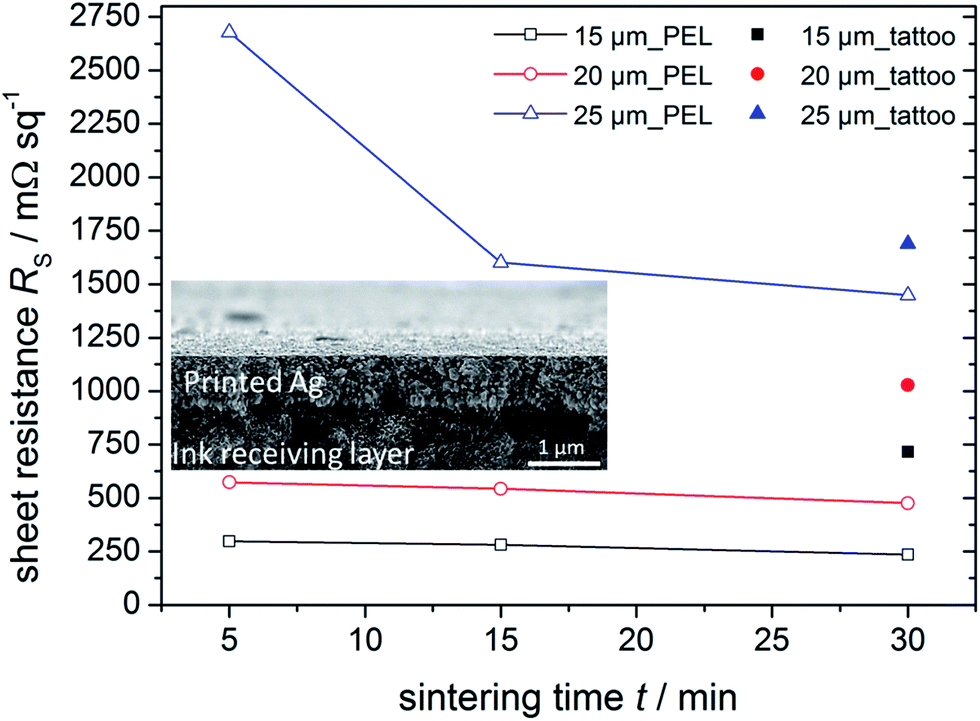 | ||
| Fig. 1 Sheet resistance of Ink A on PEL paper as function of sintering time for thermal sintering at 150 °C (open icons and solid lines) and sheet resistance of Ink A on tattoo paper after 30 min of thermal sintering at 135 °C. Cross-sectional SEM image of thermally sintered Ink A pattern (dot spacing 20 μm) on PEL paper (inset). | ||
Previous studies on Ink B have shown that good conductivity can be achieved when sintered at 150 °C for at least 30 min on glass.32 Sintering on tattoo paper at both 135 °C and 150 °C, whilst accepting substrate damage, for up to 60 min, however, gave no measurable resistance. SEM images (Fig. 2b) did not show any signs of grain coarsening but particle sizes comparable to the as-printed ink. Whilst high surface roughness and a significantly lower amount of deposited ink per layer could be reasons for the comparatively high resistance, the absence of any sintering can only be due to the paper used here. The impact of the thermal conductivity of the substrate material, for instance, is known to have a large impact on the sintering result of silver nanoparticle inks.33 As indicated in the previously reported resistivity model for this particular ink, prolonged sintering times can lead to conductive patterns at lower temperatures.32 From a processing as well as substrate damage point of view, sintering times in the range of several hours at these temperatures are, however, not compatible with low cost and high throughput production.
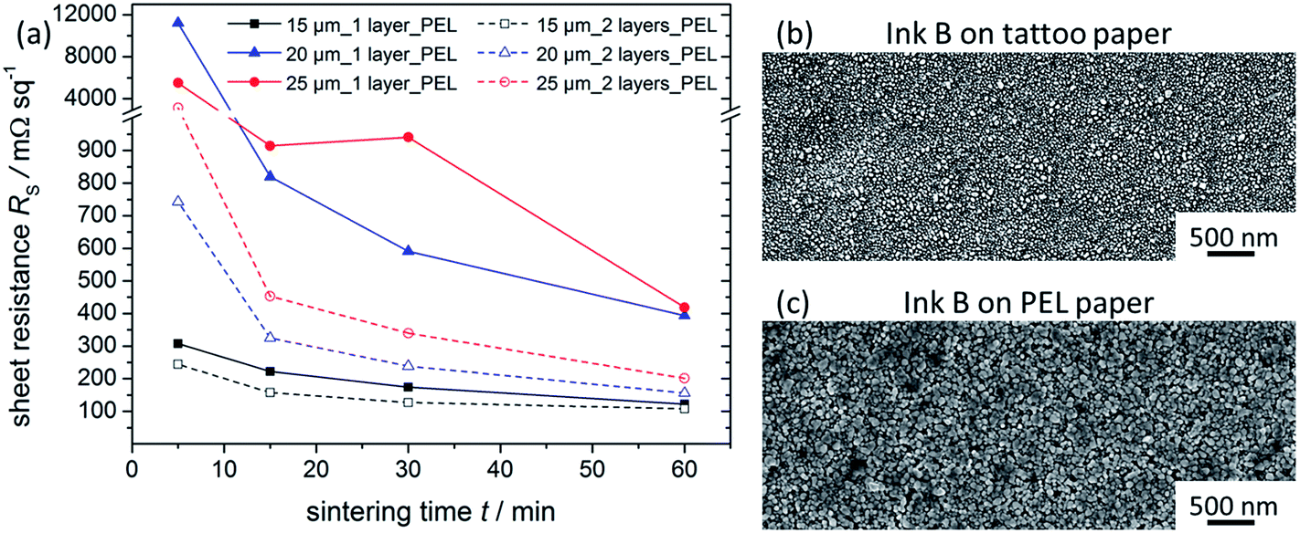 | ||
| Fig. 2 Sheet resistance of single (solid lines and icons) and double layer (dashed lines and open icons) patterns of Ink B on PEL paper as function of sintering time for thermal sintering at 150 °C (a), SEM images of thermally sintered patterns of Ink B on tattoo (b) and PEL (c) paper. | ||
In contrast to the unsuccessful sintering on tattoo paper, thermal sintering of Ink B on PEL paper using the same conditions reveals excellent sheet resistances of 174, 590 and 940 mΩ sq−1 after 30 min for single layer patterns printed with drop spacing of 15, 20 and 25 μm, respectively, with double layer printing showing a further significant resistance reduction (Fig. 2a). All samples show a significant drop in sheet resistance within the first 15 min of sintering and significant densification and grain coarsening of the nanoparticles being observed by SEM (Fig. 2c) compared with un-sintered silver nanoparticle ink.28 It has to be stated that despite any deformation of the PEL paper, significant yellowing is observed for sintering times above 15 min, indicating a slow decomposition of substrate components.
These results of Ink B on PEL and tattoo paper, in particular the differences of the SEM images, clearly show the influence of different substrate materials on the sintering performance. The silica based ink receiving layer of PEL paper is believed to have beneficial effect on the thermal sintering of nanoparticle based inks. Allen et al. reported on the sintering of a silver nanoparticle ink at room temperature and high humidity resulting in conductive patterns after one day.34 It is believed that these effects are due to synergistic enhanced water uptake by the silanol groups and a high bonding affinity of the stabilizer to the silica surface. The results for thermal sintering of Ink A and Ink B on PEL paper also reveal favorable effects in comparison to sintering on tattoo paper or on glass substrates, even without any humidity treatment.
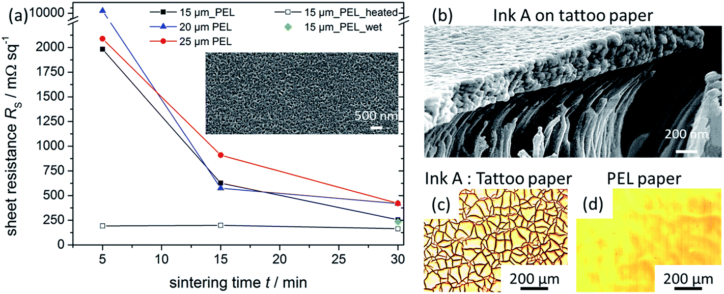 | ||
| Fig. 3 Sheet resistances of low-pressure argon plasma sintered single layer patterns of Ink A on PEL paper after pre-drying at 100 °C for 5 min (solid lines and icons), without pre-drying (green diamond data point) and in combination with a pre-heated ground platen of the plasma device (Diener pico) (a). SEM image of Ink A on top of the ink receiving layer of tattoo paper (b), microscopy images of Ink A on tattoo (c) and PEL paper after 30 min of plasma sintering (d). | ||
The results of plasma sintering of Ink B on both paper substrates are displayed in Fig. 4a. Sintered patterns did not show any signs of crack formation after sintering. Since Ink B is aqueous based, unlike Ink A which is glycol based, residual solvents can be more effectively removed from the as-printed pattern either during a pre-drying stage or during printing via elevated substrate temperatures. Due to the very high surface roughness of the printed patterns on tattoo paper, reliable sheet resistance values could not be measured and consequently the resistance values of an 8 × 0.4 mm2 line are reported in Fig. 4. For Ink B, a significant decrease in resistance is observed on both, tattoo and PEL paper, down to approximately 11.6 and 3.3 Ω, respectively. For comparison to other sintering techniques in this study, sheet resistance values of samples after 30 min of plasma sintering are provided in Fig. 4d. Plasma sintering of Ink B results in comparable values to plasma sintering of Ink A when sintered on PEL paper. Despite its rather high surface roughness on tattoo paper, Ink B shows no signs of crack formation during plasma sintering and yields improved resistance values compared to thermal sintering on tattoo as well as PEL paper.
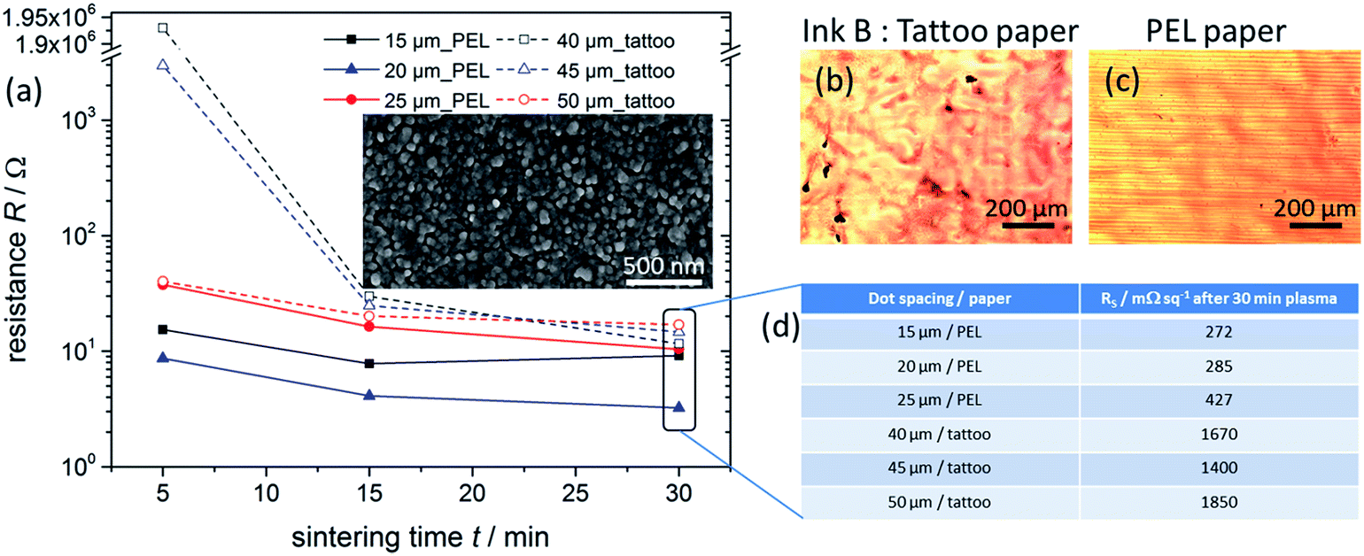 | ||
| Fig. 4 Resistances of low-pressure argon plasma sintered single layer patterns of Ink B on PEL after pre-drying (solid lines and icons) and on tattoo paper without additional pre-drying (dashed lines and open icons) (a). SEM image of plasma sintered Ink B (both papers) (a, inset). Microscopy images of plasma sintered patterns of Ink B on tattoo (b) and PEL (c) paper, corresponding sheet resistance values after 30 min of plasma sintering (Diener pico) (d). | ||
Unlike thermal sintering, lower sheet resistances upon increasing amount of deposited material was generally not observed for plasma sintering (Fig. 3a and 4a). This is because plasma sintering progresses top down with thicker layers requiring longer times for complete sintering throughout the entire layer. In combination with a heated substrate, this can be partially off-set although it is highly ink and substrate dependent as can be seen from the comparison of Fig. 3a and 4a.14,15
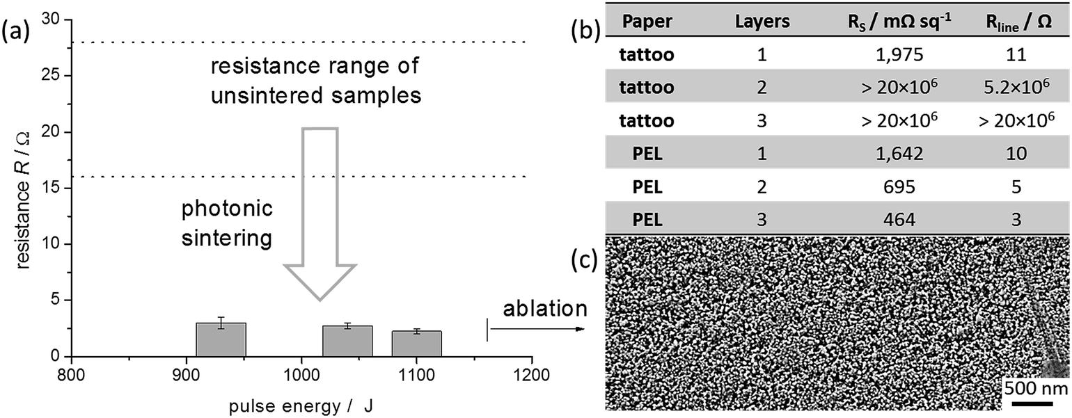
IPL sintering of single layer Ink A on PEL paper resulted in homogeneously sintered films showing successful grain coarsening and coalescence of the silver nanoparticles by SEM with few micro cracks mainly resulting from residual solvent in the printed ink (Fig. S4†), which are further reduced by pre-drying. The effect of increasing pulse energies on the resistance of Ink A on PEL paper at a belt speed of 34 mm s−1 is shown in Fig. 5a. The optimal window of operation is rather narrow, 900 to 1100 J per pulse, since at lower values no significant improvement in sheet resistance is observed, whereas higher energies increase the risk of partial ablation of the silver from the substrate, resulting in non-functional structures. For multilayer patterns, a decrease in sheet resistance with increasing number of layers is observed. Whilst in comparison to thermal and plasma sintering, IPL sintering yields slightly higher sheet resistance, the processing time is reduced by several orders of magnitude (milliseconds) demonstrating a significant step towards high-throughput production compatibility.
 | ||
| Fig. 5 Influence of varying pulse energies on the resistance of triple layer patterns of Ink A on PEL paper at a substrate speed of 34 mm s−1, a pulse frequency of 1.8 Hz and a pulse length of 2.0 ms (a). Sheet resistances of photonic sintered patterns of Ink A on tattoo and PEL paper at 20 μm dot spacing (b). SEM image of Ink A on PEL after photonic sintering (c). | ||
IPL sintering of single layer Ink A on tattoo paper gave similar results to PEL paper. However multi-layered patterns suffered severe cracking, irrespective of pre-drying, as a result of the deformation of the low Tg ink receiving layer due to an excess of heat being transferred into the substrate resulting in localized softening. Excess energy is dissipated into the top layers of the substrate material, which permanently warps, if too much energy is used during IPL sintering.37,38 Since the ink receiving layer of the tattoo paper is very thin, this particular substrate does not tolerate heat conduction of this magnitude. These findings are analogous to using too high temperatures in an oven, hence, it is believed that the poor electrical performance of multilayer structures is due to substrate damage as detailed in our previous work.8 This conclusion is further supported by microscopy images of defective patterns revealing undulated features, which are similar to the defects of the substrate observed after excessive thermal sintering (Fig. S2 and S6a†). Further optimization could potentially improve the performance of multilayer patterns.
Within this study, it was not possible to find settings to successfully sinter Ink B using IPL sintering on either of the paper substrates without significant damage (Fig. S6b and c†). As seen from the thermal sintering results Ink B requires significantly more energy input to be successfully sintered compared to Ink A supported by prior reports on polymer foil and glass.15,32,35 In order to achieve sintering of Ink B using IPL sintering, more energy has to be coupled into the ink, which directly translates into a higher temperature as well as enhanced heat dissipation into the substrate material.
3.4. UHF electromagnetic devices
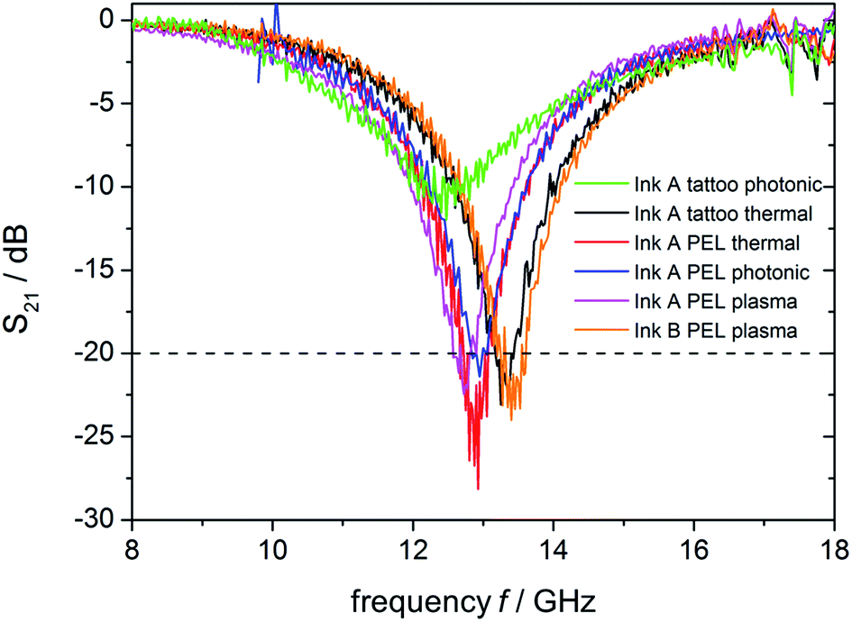 | ||
| Fig. 6 Measured transmission response (S21) of single layer FSS fabricated with Ink A on tattoo and PEL paper sintered by thermal, photonic and plasma means and Ink B on PEL paper sintered by plasma means. | ||
In comparison to small scale samples, homogeneous sintering of Ink A on tattoo paper by plasma and IPL at A4 scale proved to be difficult and yielding dipoles with many defects due to crack formation and damage to the substrate resulting in comparatively high resistances, and as a consequence, S21 were insufficient and in the range of −11 dB. This is in contrast to thermally sintered structures which gave S21 of −23 dB at about 13 GHz. Single layer plasma, IPL and thermally sintered FSS on PEL paper, however, all gave S21 of −21 to −24 dB at 15 μm drop spacing and high reflectivity of the surface at about 13 GHz. The transmission response could be further improved from −24 to −27 dB by increasing the number of deposited layers from one to three. Differences in transmission response values are attributed to differences in the electrical performance of printed dipoles achieved for each paper/sintering technique combination as detailed earlier (Table S1†). These transmission response values are comparable to those reported for the same FSS structure inkjet printed on PEN foil with a similar ink thermally sintered at 160 °C for 120 min (ref. 5) and comparable to copper wet-etched FSS (Table S1†) with the slightly different resonant frequencies a consequence of slightly different dipole lengths in the two cases.5
For Ink B, only FSS structures on PEL paper sintered via thermal and plasma sintering were considered here since a low surface roughness of the printed pattern could not be achieved by printing Ink B on tattoo paper. Whilst small area thermal sintering of Ink B on PEL paper yielded printed features of good electrical performance, 2.3 Ω per dipole, A4 FSS produced using the same optimized printing and thermal sintering procedure had a transmission response of only −11 dB, since the dipole resistances were now between 70 to 160 Ω per dipole. These adverse upscaling effects of thermal sintering are believed to be due to the higher relative volume of paper acting as a large heat sink and therefore retarding the sintering process. This effect is more pronounced in the case of Ink B because the temperatures required for sintering are significantly higher compared to Ink A.
Since plasma sintering is not based on thermal effects, heat sink effects of up-scaled are not as prevalent. Plasma sintered FSS fabricated with Ink B yielded transmission responses of −23 dB, which is comparable to those obtained for Ink A, Fig. 6. This is an encouraging result which demonstrates that functional electromagnetic devices of similar performance are not limited to simply one ink. Sintering, however, has to be adapted according to the used ink/substrate combination.
Single layer antennas were printed on tattoo paper, pre-dried at 70 °C and subsequently processed via low-pressure argon plasma (Diener nano, 30 min) and IPL sintering. After application of the integrated circuit (IC) chip to the port area of the antenna, the tag was transferred to the forearm of a volunteer and investigated regarding read range at different frequencies. The functionality of the RFID tags relies on high conductivity of the antenna system, particularly on the feed track of the port area. Therefore, a low port-to-port resistance (Rp2p) is desired and taken as reference resistance in this study. As shown in Table 1, antennas fabricated by plasma and IPL sintering methods resulted in UHF RFID tags of substantially superior read distance, 46 and 50 cm initial read range respectively, to those fabricated by thermal sintering 12 cm and of equal or superior performance to those fabricated using stencil applied silver paste 45 cm. This is attributed to the comparatively improved electrical properties, Rp2p, of the antennas, whilst the lower Rp2p and higher read distance of the copper etched tag, 75 cm, is in part due to its greater layer thickness (≥18 μm) in comparison to the inkjet printed antennas (<1 μm). Although multilayer printing can lead to improved electrical performance and, hence, improved read range, this has an associated cost penalty. Plasma and especially photonic sintering, which is a process that takes just a few seconds, can contribute to reducing sintering time and, hence, manufacturing costs.
| Material | Fabrication | Sintering | Ink layers | R p2p/Ω | Read distancea/cm | Ref. |
|---|---|---|---|---|---|---|
| a Within designated UHF RFID bands: 865 to 868 MHz for Europe and 902 to 928 MHz for North America. | ||||||
| Ink A | Inkjet | Plasma | 1 full antenna | 17 | 46 | — |
| Ink A | Inkjet | IPL | 1 full antenna | 12 | 50 | — |
| Ink A | Inkjet | Thermal | 1 full antenna | 116 | 12 | 9 |
| Silver paste | Stencil | N/A | 1 full antenna | 27 | 45 | 39 |
| Cu metal | Etching | N/A | 1 full antenna | 0.17 | 75 | 39 |
4. Conclusions
From consideration of two different silver nanoparticle inks on two different substrates we see that the effectiveness of the sintering approach is highly dependent on the matched properties of both ink and substrate material. An overview of the sintering results obtained are shown in Table 2, demonstrating that the applied sintering technology has to be carefully chosen for each ink/substrate combination in order to obtain optimal electrical properties of the printed patterns.| Thermal sintering | Plasma sintering | IPL sintering | ||||||||||
|---|---|---|---|---|---|---|---|---|---|---|---|---|
| Substrate | Tattoo | PEL | Tattoo | PEL | Tattoo | PEL | ||||||
| a Resistance values in Ω due to high surface roughness; ✗ – no measurable conductivity after sintering. | ||||||||||||
| Ink | A | B | A | B | A | Ba | A | Ba | A | B | A | B |
| Successful sintering | ✓ | ✗ | ✓ | ✓ | ✓ | ✓ | ✓ | ✓ | ✓ | ✗ | ✓ | ✗ |
| Timescale/min | 30 | — | <30 | 5 | 30 | 15 | 15 | 5 | <1 s | — | <1 s | — |
| Min. Rsq/mΩ sq−1 | 716 | — | 236 | 174 | 300 | 15 Ω | 255 | 3 Ω | 1975 | — | 464 | — |
The comparison of the different paper substrates revealed that PEL paper with its micro porous inorganic ink receiving layer is more stable under all applied sintering conditions, whereas tattoo paper is more heat sensitive due to the thin polymer receiving layer, which does not tolerate temperatures above 100 °C for an extended amount of time. Therefore, global or selective heating often resulted in damaged substrate and sintered pattern and sintering temperatures and conditions have to be chosen as mild as possible.
Optimized conditions for each ink/paper/sintering combination were subsequently used for the manufacturing of FSS and RFID devices. This work demonstrates that single layer FSS and RFID conductive features can be produced on paper substrates via inkjet printing in combination with thermal and alternative sintering techniques compatible with R2R manufacturing. The performance of the FSS arrays meets real-life requirements for application in the field of wireless communication. We have furthermore demonstrated that the performance of the FSS presented here can be improved by adopting a multilayer printing approach by increasing the amount of deposited material. Triple layer FSS show transmission responses that are superior to previously reported inkjet printed FSS on PEN foil and comparable to copper etched according to the same design (Table S1†). Furthermore, it was found that on-skin RFID tags manufactured via inkjet printing and using plasma and IPL sintering methods show superior electrical and, hence, greater read distance performance compared to RFID tags previously produced by inkjet manufacturing. Although processing conditions have to be chosen carefully for the heat sensitive tattoo paper, the successful manufacturing of both, FSS and RFID tags on such a transferable substrate demonstrates the possibility of applying such devices on different surfaces such as walls, windows or on-skin.
For the fabrication of paper based FSS arrays and RFID antennas, inkjet printing is a promising tool since it allows simple design alteration and adaption of layer thicknesses in order to tailor the properties of electromagnetically active structures to specific applications. Furthermore, recent developments in alternative sintering approaches show the potential to be used as fast and substrate friendly sintering technique allowing high throughput production in the near future.9,26,28,34
Acknowledgements
The authors thank Matthias Hartlieb and Stefan Hölzer from the Friedrich Schiller University Jena for assistance with the plasma sintering experiments. Veronica Sanchez-Romaguera, Daniel Tate Badredin Turki and Dumtoochukwu Oyeka would like to thank EPSRC for funding (EP/J000825/1 and EP/K03099X/1). Authors would like to thank Prof. Madgassi for kindly providing Ink B. Veronica Sanchez-Romaguera and Sebastian Wünscher contributed equally to this work.References
- J. A. Arnaud and J. T. Ruscio, Electron. Lett., 1973, 9, 589–590 CrossRef.
- L. E. Comtesse, R. J. Langley, E. A. Parker and J. C. Vardaxouglou, in Proc. 17th European Mircowave Conf., Rome, 1987, vol. 9, pp. 2008–2013 Search PubMed.
- A. H. Wong, M. J. Neve and K. W. Sowerby, in Proc. IEEE Antenn. Propag. Soc. Int. Symp., Washington, CA, USA, 2005, vol. 1A, pp. 779–802 Search PubMed.
- E. A. Parker, J. B. Robertson, B. Sanz-Izquierdo and J. C. Batchelor, Electron. Lett., 2008, 44, 394–395 CrossRef CAS.
- J. C. Batchelor, E. A. Parker, J. A. Miller, V. Sanchez-Romaguera and S. G. Yeates, Electron. Lett., 2009, 45, 78 CrossRef.
- W. G. Whittow, Y. Li, R. Torah, K. Yang, S. Beeby and J. Tudor, Electron. Lett., 2014, 50, 916–917 CrossRef.
- S. Kim, B. Cook, T. R. Le, J. Cooper, H. Lee, V. Lakafosis, R. Vyas, R. Moro, M. Bozzi, A. Georgiadis, A. Collado and M. M. Tentzeris, IET Microwaves, Antennas and Propagation, 2013, 7, 858–868 CrossRef PubMed.
- V. Sanchez-Romaguera, M. A. Ziai, D. Oyeka, S. Barbosa, J. S. R. Wheeler, J. C. Batchelor, E. A. Parker and S. G. Yeates, J. Mater. Chem. C, 2013, 1, 6395–6402 RSC.
- S. Wünscher, R. Abbel, J. Perelaer and U. S. Schubert, J. Mater. Chem. C, 2014, 2, 10232–10261 RSC.
- J. Perelaer, A. W. M. de Laat, C. E. Hendriks and U. S. Schubert, J. Mater. Chem., 2008, 18, 3209–3215 RSC.
- S. Magdassi, M. Grouchko, O. Berezin and A. Kamyshny, ACS Nano, 2010, 4, 1943–1948 CrossRef CAS PubMed.
- S. M. Bidoki, D. M. Lewis, M. Clark, A. Vakorov, P. A. Millner and D. McGorman, J. Micromech. Microeng., 2007, 17, 967–974 CrossRef CAS.
- M. L. Allen, M. Aronniemi, T. Mattila, A. Alastalo, K. Ojanperä, M. Suhonen and H. Seppä, Nanotechnology, 2008, 19, 175201 CrossRef PubMed.
- I. Reinhold, C. E. Hendriks, R. Eckardt, J. M. Kranenburg, J. Perelaer, R. R. Baumann and U. S. Schubert, J. Mater. Chem., 2009, 19, 3384–3388 RSC.
- J. Perelaer, R. Abbel, S. Wünscher, R. Jani, T. van Lammeren and U. S. Schubert, Adv. Mater., 2012, 24, 2620–2625 CrossRef CAS PubMed.
- J. Perelaer, B.-J. de Gans and U. S. Schubert, Adv. Mater., 2006, 18, 2101–2104 CrossRef CAS.
- D. Tobjörk, H. Aarnio, P. Pulkkinen, R. Bollström, A. Määttänen, P. Ihalainen, T. Mäkelä, J. Peltonen, M. Toivakka, H. Tenhu and R. Österbacka, Thin Solid Films, 2012, 520, 2949–2955 CrossRef PubMed.
- T. Kumpulainen, J. Pekkanen, J. Valkama, J. Laakso, R. Tuokko and M. Mäntysalo, Opt. Laser Technol., 2011, 43, 570–576 CrossRef CAS PubMed.
- H.-S. Kim, S. R. Dhage, D.-E. Shim and H. T. Hahn, Appl. Phys. A, 2009, 97, 791–798 CrossRef CAS PubMed.
- R. Abbel, T. van Lammeren, R. Hendriks, J. Ploegmakers, E. J. Rubingh, E. R. Meinders and W. A. Groen, MRS Commun., 2012, 2, 145–150 CrossRef CAS.
- Y. Amin, Q. Chen, L. R. Zheng and H. Tenhunen, Prog. Electromagn. Res., 2012, 130, 241–256 CrossRef.
- N. Thi Thi, M. Nogi and K. Suganuma, J. Mater. Chem. C, 2013, 1, 5235–5243 RSC.
- T. Öhlund, J. Örtegren, S. Forsberg and H.-E. Nilsson, Appl. Surf. Sci., 2012, 259, 731739 CrossRef PubMed.
- L. Xie, M. Mäntysalo, A. López Cabezas, Y. Feng, F. Jonsson and L.-R. Zheng, Mater. Lett., 2012, 88, 68–72 CrossRef CAS PubMed.
- J. Niittynen, R. Abbel, M. Mäntysalo, J. Perelaer, U. S. Schubert and D. Lupo, Thin Solid Films, 2014, 556, 452–459 CrossRef CAS PubMed.
- A. Kamyshny and S. Magdassi, Small, 2014, 10, 3515–3535 CrossRef CAS.
- R. Abbel, T. van Lammeren, R. Hendriks, J. Ploegmakers, E. J. Rubingh, E. R. Meinders and W. A. Groen, MRS Commun., 2012, 2, 145–150 CrossRef CAS.
- R. Abbel, P. Teunissen, E. Rubingh, T. Van Lammeren, R. Cauchois, M. Everaars, J. Valeton, S. van de Geijn and P. Groen, Transl. Mater. Res., 2014, 1, 015002 CrossRef.
- M. Turki, E. A. Parker, J. C. Batchelor, M. A. Ziai, V. Sanchez-Romaguera and S. G. Yeates, Electron. Lett., 2013, 49, 1054–1055 CrossRef.
- http://www.printedelectronics.co.uk/Information%20Sheet%20for%20PEL%20Nano%20P60.pdf .
- L. Goehring, R. Conroy, A. Akhter, W. J. Clegg and A. F. Routh, Soft Matter, 2010, 6, 3562–3567 RSC.
- J. F. Salmerón, F. Molina-Lopez, D. Briand, J. J. Ruan, A. Rivadeneyra, M. A. Carvajal, L. F. Capitan Vallvey, N. F. Derooij and A. J. Palma, J. Electron. Mater., 2014, 43, 604–617 CrossRef PubMed.
- K. C. Yung, X. Gu, C. P. Lee and H. S. Choy, J. Mater. Process. Technol., 2010, 210, 2268–2272 CrossRef CAS PubMed.
- M. Allen, J. Leppäniemi, M. Vilkman, A. Alastalo and T. Mattila, Nanotechnology, 2010, 21, 475204 CrossRef PubMed.
- S. Wünscher, B. Seise, D. Pretzel, S. Pollok, J. Perelaer, K. Weber, J. Popp and U. S. Schubert, Lab Chip, 2014, 14, 392–401 RSC.
- M. Frenkel, in The Chemistry of Inkjet Inks, ed. S. Magdassi, World ScientificPublishing Co. Pte. Ltd., Singapore, 2010, pp. 73–97 Search PubMed.
- K. A. Schroder, in Proc. NSIT Int. Nanotech. Conf., 2011, p. 220 Search PubMed.
- M. J. Guillot, S. C. McCool and K. A. Schroder, in Proc. 12th Int. Conf. Nucl. Engin.IMECE12 87674, 2012, vol. 7, pp. 19–27 Search PubMed.
- M. A. Ziai and J. C. Batchelor, IEEE Trans. Antennas Propag., 2011, 59, 3565–3571 CrossRef.
Footnote |
| † Electronic supplementary information (ESI) available. See DOI: 10.1039/c4tc02693d |
| This journal is © The Royal Society of Chemistry 2015 |