
 Open Access Article
 This Open Access Article is licensed under a
 Creative Commons Attribution 3.0 Unported Licence
Chemical vapour deposition of antimony chalcogenides with positional and orientational control: precursor design and substrate selectivity†
S. L.
Benjamin
a,
C. H.
de Groot
b,
A. L.
Hector
a,
R.
Huang
b,
E.
Koukharenko
b,
W.
Levason
a and
G.
Reid
*a
aChemistry, University of Southampton, SO17 1BJ, UK. E-mail: G.Reid@soton.ac.uk
bElectronics and Computer Science, University of Southampton, SO17 1BJ, UK
First published on 11th November 2014
Abstract
A series of alkylchalcogenostibines, Me2SbSenBu, MeSb(SenBu)2, Sb(SenBu)3 and MeSb(TenBu)2, have been designed and synthesised as potential precursors for chemical vapour deposition (CVD) by reaction of nBuELi (E = Se, Te) with the appropriate halostibine, Me3−nSbCln (n = 1, 2, 3), and characterised by 1H, 13C{1H} and 77Se{1H} or 125Te{1H} NMR spectroscopy as appropriate. MeSb(SenBu)2 and MeSb(TenBu)2 are very effective single source precursors for the low pressure CVD of high quality crystalline thin films of Sb2Se3 and Sb2Te3, respectively, confirmed by scanning electron microscopy, energy dispersive X-ray spectroscopy, Raman spectroscopy and thin film X-ray diffraction. Hall conductivity, carrier mobility, carrier density and, in the case of Sb2Te3, Seebeck coefficient measurements reveal electronic characteristics comparable with Sb2E3 deposited by atomic layer deposition or molecular beam epitaxy, suggesting materials quality and performance suitable for incorporation into electronic device structures. Choice of substrate and deposition conditions were found to significantly affect the morphology and preferred orientation of Sb2Te3 crystallites, enabling deposition of films with either 〈1 1 0〉 or 〈0 0 1〉 alignment. Use of micro-patterned substrates allowed selective deposition of crystalline 2D micro-arrays of Sb2Te3 onto exposed TiN surfaces only.
Introduction
Antimony chalcogenides Sb2E3 (E = Se, Te) are versatile semiconductor materials with narrow bandgaps, which are increasingly demonstrating potential in a diversity of microelectronic applications, especially in low dimensional forms. The most established of these is as thermoelectric materials with moderate figures of merit (ZT), often combined with Bi2E3 in thermoelectric devices for near room temperature applications.1 Thermoelectrics have the potential to provide a source of sustainable, emission-free energy or cooling, but advances are required to improve current material efficiencies. Controlling the dimensionality in such materials can lead to significant improvements in ZT,2 and superlattices of Sb2Te3 and Bi2Te3 have been claimed to have among the highest ZT values ever recorded.3 Anisotropy of the thermal and electrical parameters in the layered lattice structures of these materials means that control over crystallite orientation offers another route to maximise ZT.4–6 In addition, Sb2Te3 is a topological insulator, with potential applications in quantum computing.7 Exploitation of this effect requires single crystals of the binary material; confinement to the nanoscale maximises the surface to volume ratio, preventing topological surface states from being dominated by bulk conduction states.8 Finally, Sb2Se3 has received considerable recent attention as an efficient light sensitiser, which can be incorporated as a thin film into multilayer photovoltaic devices.9,10Chemical vapour deposition (CVD) is a technique widely used industrially to deposit thin films of a range of materials, including binary semiconductors, due to the scalable and cost-effective nature of the process. The potential of employing CVD as an effective route to low dimensional Sb2E3 has been little explored. One very recent approach employs iPr3Sb and Et2Te2 as dual source precursors for the metal–organic (MO) CVD of flat films of Sb2Te3.11 Single source precursors (SSPs) are a promising alternative for these systems, as they improve ease of handling and atom efficiency while allowing properties such as stoichiometry and morphology to be directed by precursor design.12,13 There are very few examples of the use of SSPs for the deposition of Sb2E3. Individual Sb2Te3 nanoplates and Sb2Se3 nanorods have been synthesised by aerosol assisted (AA) CVD from [Sb{(TePiPr2)2N}3] and [Sb{SeC5H3(Me-3)N}3] respectively, the latter being a very rare example of the preparation of Sb2Se3 by CVD.14,15 Preliminary investigations into the use of the organometallic species Et2SbTeEt and Te(SbEt2)2 as SSPs in AACVD did not yield stoichiometric Sb2Te3.16 However, Te(SbEt2)2 was employed successfully as a SSP in the synthesis of Sb2Te3 nanoplates by thermal decomposition methods,17 and recent studies have shown that CVD from the same precursor gives poorly aggregated Sb2Te3 films at 200 °C, with antimony-rich films being obtained at higher temperatures.18
We have previously developed systems for low pressure (LP) CVD of metal chalcogenide thin films from coordination complexes with neutral chalcogenoether ligands.19–22 In these systems we found that precursors containing –EnBu groups (E = Se, Te) out-perform those with shorter alkyl or aryl groups at the chalcogen, giving uniform thin films of high quality. Coordination complexes of heavy p-block metals with chalcogen containing ligands have some potential disadvantages when considered as precursors for LPCVD, namely their relatively low volatilities, resulting in short deposition path lengths and reduced atom efficiency, and the presence of halides or other elements which in some circumstances can act as undesirable contaminants, severely diminishing electronic performance. Organometallic species containing bonds between p-block elements with only hydrocarbon substituents present a potential solution to these challenges.
As a result of these considerations, we identified compounds of the form R3−nSb(EnBu)n for development as improved precursors for LPCVD. Here we report the synthesis of a new series of these compounds and their employment for the CVD of high quality, uniform, polycrystalline Sb2E3 thin films. Modifications in precursor design allow optimisation of stoichiometry and coverage, while variations in substrate and temperature give remarkable control over film morphology and crystallite orientation, including fabrication of micro-scale arrays.
Results and discussion
Synthesis of tailored single source precursors
The selenostibines, Me2SbSenBu, MeSb(SenBu)2 and Sb(SenBu)3, were prepared by generating nBuSeLi in situ23 and reacting this with the appropriate chlorostibine (Scheme 1). | ||
| Scheme 1 Synthesis of alkylselenostibines. | ||
Molecules of the type R2SbSeR′ (R = Me, Et; R′ = Me, Ph) have previously been synthesised by the comproportionation of R2SbSbR2 with R′SeSeR′,24,25 and one structure (R = R′ = Me) has been determined by gas phase electron diffraction.26 Heating of these compounds over a period of hours gives RSb(SeR′)2 and SbR3.27 The only previously reported species of the form Sb(SeR)3 (R = alkyl) is Sb(SeMe)3, which was synthesised by reflux of elemental Sb with Me2Se2 in toluene. The crystal structure shows the presence of weak intermolecular Sb⋯Se contacts which form a 2D sheet.28
The three new selenostibines with varying Sb![[thin space (1/6-em)]](https://www.rsc.org/images/entities/char_2009.gif) :Se ratios (1:1, 1:2 and 1:3) were tested as precursors for the LPCVD of Sb2Se3 under varying conditions. All three precursors deposited grey thin films onto fused SiO2 substrates at 500 °C, which were observed by scanning electron microscopy (SEM) to be composed of rod-like crystallites. Energy dispersive X-ray spectroscopy (EDX) demonstrated that both Sb and Se were present in all films, however those deposited from Me2SbSenBu had a variable Sb:Se ratio which was generally high in Sb (around 1:1), whereas those deposited from MeSb(SenBu)2 and Sb(SenBu)3 had Sb:Se ratios close to the desired 1:1.5. Of these, MeSb(SenBu)2 gave films of consistently superior uniformity and coverage, probably due to its higher volatility, and as a result this was the precursor selected for further study (vide infra). These results demonstrate how stoichiometry and morphology of thin films deposited by CVD can be manipulated by the modification of single source precursor design.
:Se ratios (1:1, 1:2 and 1:3) were tested as precursors for the LPCVD of Sb2Se3 under varying conditions. All three precursors deposited grey thin films onto fused SiO2 substrates at 500 °C, which were observed by scanning electron microscopy (SEM) to be composed of rod-like crystallites. Energy dispersive X-ray spectroscopy (EDX) demonstrated that both Sb and Se were present in all films, however those deposited from Me2SbSenBu had a variable Sb:Se ratio which was generally high in Sb (around 1:1), whereas those deposited from MeSb(SenBu)2 and Sb(SenBu)3 had Sb:Se ratios close to the desired 1:1.5. Of these, MeSb(SenBu)2 gave films of consistently superior uniformity and coverage, probably due to its higher volatility, and as a result this was the precursor selected for further study (vide infra). These results demonstrate how stoichiometry and morphology of thin films deposited by CVD can be manipulated by the modification of single source precursor design.
Given the identification of MeSb(SenBu)2 as the most effective precursor for the CVD of Sb2Se3, the analogous tellurostibine, MeSb(TenBu)2, was targeted as the precursor of choice for the CVD of Sb2Te3. It was prepared by the addition of 0.5 mol. equiv. of MeSbCl2 to a freshly prepared solution of nBuTeLi29 at −78 °C (Scheme 2).
 | ||
| Scheme 2 Synthesis of MeSb(TenBu)2. | ||
The 1H NMR spectrum shows a singlet corresponding to the MeSb group, with four multiplets corresponding to the nBuTe groups, in the expected ratios, and a singlet evident in the 125Te{1H} NMR spectrum at 107 ppm. A minor peak at 230 ppm was identified as a small amount of TenBu2, peaks corresponding to which could also be discerned as minor features in the 1H NMR spectrum. Attempted purification by distillation resulted in decomposition of the majority of the compound. The crude product was used for all CVD experiments described below, with no obvious detriment arising from the presence of the minor telluroether impurity. Though sensitive to both atmosphere and temperature (an insoluble dark brown substance forms upon air exposure or storage over days at room temperature), MeSb(TenBu)2 is stable over periods of months when stored under N2 at −18 °C. Related compounds, RSb(TeR′)2, have been prepared previously by oxidative addition of cyclic or polymeric (RSb)n across diorganoditellurides, R′TeTeR′.25,30,31 In some cases this reaction was reported to be reversible in solution, though we found no evidence for the formation of nBuTeTenBu from solutions of MeSb(TenBu)2.30 The compound MeSb(TenBu)2 is somewhat thermochromic, appearing as a bright red oil at room temperature, but reversibly darkening to a black-brown solid below ∼0 °C. Thermochromism has also been reported for related tellurostibines, R2SbTeMe (R = Me, Et).32
Materials deposition and characterisation
 | ||
| Fig. 1 SEM images of Sb2Te3 films deposited by CVD onto fused SiO2 substrates; tile (a) in hotter zone; tile (b) in cooler zone. | ||
The peaks for these elements overlap in the EDX spectrum; quantitative WDX calibrated against elemental standards gives Sb:Te = 41.9:58.1, which is in close agreement with the expected value of 40:60. No peak corresponding to C was identified in the EDX analysis, and combustion analysis performed on Sb2Te3 powder separated from the substrate gave a C content of 0.74%. When deposition occurs onto fused silica substrates, good coverage is observed over up to 7 tiles (placed in a heated zone between 1 cm and 14 cm from the precursor). In our system, proximity to the precursor and precise substrate temperature are inseparably correlated, with tiles furthest from the precursor occupying the hottest zone of the tube furnace (Fig. 2).
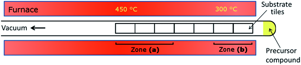 | ||
| Fig. 2 Schematic of LPCVD reactor with positions of zones (a) and (b) indicated. | ||
Films deposited onto fused silica substrates positioned in this hotter zone (450 °C) (a) are flattest, with SEM images showing the hexagonal faces of many of the Sb2Te3 crystallites lying parallel to the substrate surface (Fig. 1a). In contrast, films deposited in the cooler zone (around 300 °C) closer to the source of precursor (b) are roughest, with SEM showing interpenetrating crystallites standing on end with their hexagonal faces approximately perpendicular to the surface (Fig. 1b). This disparity is observed regardless of quantity of precursor or deposition time.
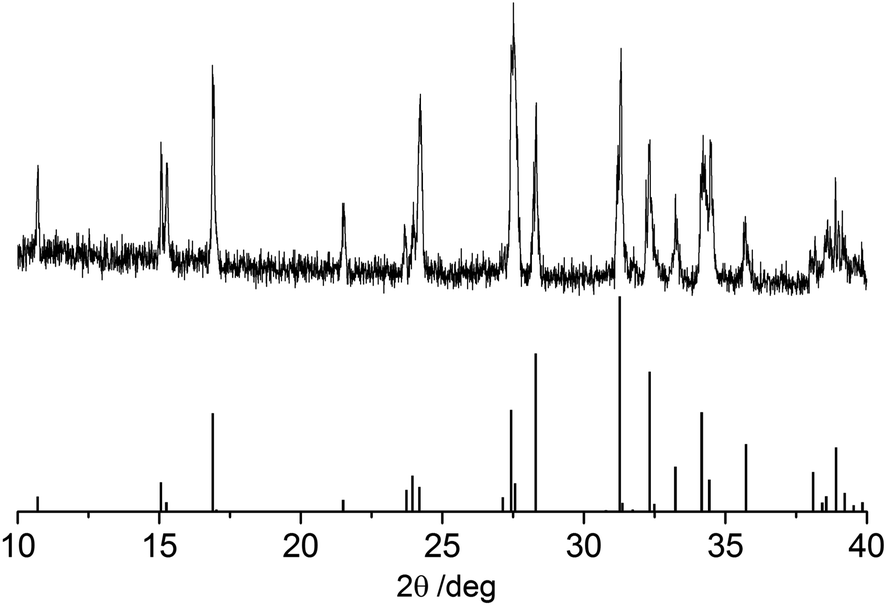
Symmetric (θ–2θ) X-ray diffraction (XRD) patterns of these films show the same single phase of Sb2Te3 (R![[3 with combining macron]](https://www.rsc.org/images/entities/char_0033_0304.gif) mh), with peak positions that correspond well with literature values (Fig. 3, see ESI† for lattice parameters).33 However, there are marked differences in the intensities of the peaks for films (a) and (b) in comparison with one another and with the literature pattern for bulk Sb2Te3.
mh), with peak positions that correspond well with literature values (Fig. 3, see ESI† for lattice parameters).33 However, there are marked differences in the intensities of the peaks for films (a) and (b) in comparison with one another and with the literature pattern for bulk Sb2Te3.
 | ||
| Fig. 3 θ–2θ XRD data for Sb2Te3 deposited by CVD onto fused SiO2 substrates in zone (a) and zone (b); database pattern for Sb2Te3 from ref. 33. Indices shown above. | ||
Pole figures were collected on key reflections for both films, confirming that the disparities in intensity are due to preferred orientation of the crystallites. The symmetric XRD pattern (Fig. 3a) of film (a), which appears flatter by SEM, shows a significant enhancement of the 0 0 l reflections. A pole figure at the 2θ position of the 0 0 15 reflection (2θ = 44.7°) shows a sharp maximum at α = 90° (Fig. 4.1), whereas that for the 1 0 10 reflection (2θ = 38.3°) has a sharp ring at 51° (Fig. 4.2), observations which are commensurate with a 〈0 0 1〉 fibre texture, in which the c-axes of the crystallites are oriented perpendicular to the substrate and the hexagonal (a and b) faces of each plate lie flat against the surface (calculated values for α in 〈0 0 1〉 orientation: 0 0 15 α = 90°; 1 0 10 α = 50.5°).
 | ||
| Fig. 4 3D pole figure projections with cut lines: 1. tile (a), 0 0 15; 2. tile (a) 1 0 10; 3. tile (b) 1 1 0; 4. tile (b) 1 0 10. | ||
In contrast, the symmetric XRD pattern for film (b) shows a significant enhancement of the 1 1 0 reflection and a corresponding suppression of the 0 0 l reflections, with a pole figure on the 1 1 0 reflection (2θ = 42.3°) this time showing a peak at 90° (Fig. 4.3), whereas the ring in the pole figure for the 1 0 10 refection is now seen at around 29° (Fig. 4.4). This is evidence that the crystallites in film (b) have 〈1 1 0〉 preferred orientation, opposite to that seen in film (a), with the c-axis parallel to the surface of the substrate (calculated values for α in 〈1 1 0〉 orientation: 1 1 0, α = 90°; 1 0 10, α = 29.5°), in accord with observations from the SEM images of hexagonal platelets standing on end. The broader peak shapes in the pole figures of film (b) suggest that the degree of orientation is not as high as indicated by the very sharp peaks in those of film (a).
In order to provide a direct comparison for patterned substrates (vide infra), films were also deposited onto substrates manufactured by coating a 1 μm thick layer of silica onto a silicon wafer by physical vapour deposition (henceforth referred to as ‘PVD silica’ substrates). Under identical deposition conditions these films had somewhat patchier coverage than those deposited onto fused silica, and SEM images show that they have yet a different morphology, now comprising stacks of thin hexagonal plates (Fig. 5).
 | ||
| Fig. 5 Top down (left) and cross sectional (right) SEM images of Sb2Te3 film deposited onto PVD silica substrates. | ||
The XRD pattern demonstrates the same crystalline phase as those deposited onto fused silica (Fig. S4 ESI†), with an enhancement of the 0 0 l peaks, suggesting that the majority of the crystals have their c-axes oriented at 90° to the substrate, including those substrates deposited in zone (a). It would appear that variation in substrate texture or surface termination can appreciably affect the morphology of these deposits onto substrates which are otherwise chemically almost identical. This ability to control crystallite orientation could be highly advantageous for thermoelectric applications, providing an effective way to optimise anisotropic thermal and electrical parameters.
Cross-sectional images were obtained by snapping the tiles after deposition. The film thickness was found to be around 2.2 μm, with layered stacks of crystallites visible side on (Fig. 5).
Raman measurements on these thin films reveal three main peaks positioned at 120, 138, and 165 cm−1, respectively (Fig. 6). These are in good agreement with the E2g, A2u and A1g vibration modes of Sb2Te3 previously reported.34
 | ||
| Fig. 6 Raman spectrum of Sb2Te3 thin film. | ||
The electronic and thermal properties of the Sb2Te3 thin films were also investigated. Hall effect measurements show the deposited Sb2Te3 to be p-type semiconductor with a charge carrier density of p = 4.73 × 1019 cm−3. A charge carrier mobility of μ = 138 cm2 V−1 S−1 was measured, yielding an electrical conductivity of σ = 1010 S cm−1. The Seebeck coefficient of the material (deposited in zone (b)) was measured to be 90 μV K−1. These values are comparable with Sb2Te3 deposited from other techniques such as molecular beam epitaxy35 and atomic layer deposition,36 although lower than the values obtained for perfectly stoichiometric Sb2Te3 deposited at low temperature.37 These results suggest that the material deposited by CVD is of quality suitable for thermoelectric and microelectronic applications.
 | ||
| Fig. 7 SEM images of patterned deposits of Sb2Te3; (a) well filled trenches. (b) Sparingly filled pattern. | ||
Patterns of squares, circles and trenches with dimensions between 100 μm and 1 μm were filled in this way. EDX mapping of 70–100 μm arrays confirms that Sb and Te are confined to the TiN areas of the pattern, surrounded by uncoated silica surface (Fig. 8). By controlling the quantity of precursor, the thickness of these deposits can be varied from those which protrude significantly from the surrounding silica (Fig. 7a), to very thin layers of crystals which lie flat on the base of the TiN wells (Fig. 7b). This type of substrate selectivity is very unusual for CVD methods, having previously only been observed using coordination complexes of chalcogenoethers as SSPs. The ability to achieve these levels of control in this system highlights the power of using SSPs in an LPCVD framework.
 | ||
| Fig. 8 (a) SEM image of Sb2Te3 array; (b) EDX mapping of Sb (red); (c) Te (green); (d) Si (magenta). | ||
 | ||
| Fig. 9 (a) Top down and (b) cross sectional SEM images of Sb2Se3 film deposited onto PVD silica substrates. | ||
EDX gives a mean Se/Sb ratio of 1.46, close to the expected value of 1.50 (Fig. S3 ESI†). Grazing incidence powder X-ray diffraction matches the literature pattern for orthorhombic Sb2Se3 with small variations in peak intensity likely due to a limited degree of preferred orientation (Fig. 10).38
 | ||
| Fig. 10 Grazing incidence (2θ) X-ray diffraction pattern of Sb2Se3 film (top), literature pattern for Sb2Se3 from ref. 38 (bottom). | ||
The Raman spectrum of the Sb2Se3 thin films was collected (Fig. 11); this is in good agreement with previously reported data.39 The main feature at about 190 cm−1 is the characteristic of the Sb–Se stretching mode of the SbSe3/2-pyramids.40 The peak at ∼150 cm−1 can be associated to the Sb–Sb bonds and the vibration at around 125 cm−1 is related to the Se–Se bonds. These three peaks can be assigned as the A21g, A22u, and E2g vibration mode, respectively.41
 | ||
| Fig. 11 Raman spectrum of Sb2Se3 thin film. | ||
Hall effect measurements conducted on the Sb2Se3 films reveal a conductivity of σ = 1.14 × 10⁻⁶ S cm−1. The low value of conductivity matches well with the wide band gap (1.1 eV) reported for Sb2Se3.42 These measurements also confirmed the Sb2Se3 to be a p-type semiconductor with carrier density and carrier mobility of 5.75 × 1011 cm−3 and 14.2 cm2 V−1 S−1, respectively. However, these films were found to be quite brittle and poorly adhered to the substrate, and hence reliable measurement of the Seebeck coefficient was not possible. It is clear from cross-sectional SEM images (Fig. 9b) that the films are composed of loosely packed large (∼5 μm long) individual rod-shaped crystallites, leading to a film of low density and with non-uniform thickness.
Substrate effects were once again probed by the use of patterned substrates. Marked differences were observed in the morphology of Sb2Se3 deposited onto TiN areas of the substrates compared to silica areas (Fig. 12), though substrate selectivity comparable to that seen for Sb2Te3 was not observed. Instead, even under precursor limited conditions, some deposition occurs on both surfaces; on SiO2 this consists of separated clusters of Sb2Se3 crystallites, whereas on TiN a continuous thin film of smaller crystallites is observed. This suggests that TiN is a promising material on which to deposit more uniform and well adhered thin films of Sb2Se3.
 | ||
| Fig. 12 Sb2Se3 deposited across a boundary between SiO2 area (left) and TiN area (right) of patterned substrate. | ||
Experimental
Precursor preparation and characterisation
Reactions were conducted using Schlenk, vacuum line and glove-box techniques under a dry nitrogen atmosphere. The reagents were stored and manipulated using a glove box. Hexane was distilled from Na wire; THF was distilled from Na/benzophenone ketyl. nBuLi (1.6 M solution in hexanes) was obtained from Acros and used as received. SbCl3 was obtained from Sigma-Aldrich and sublimed in vacuo prior to use. Me2SbCl and MeSbCl2 were prepared by treatment of Me2SbPh and MeSbPh2 with HCl, according to the literature method.43 The 1H, 13C{1H}, 77Se{1H} and 125Te{1H} NMR spectra were recorded at 298 K in CDCl3 using a Bruker DPX400 spectrometer and referenced to the residual protio-solvent resonance, neat SeMe2 and neat TeMe2 respectively. Microanalyses were undertaken by Medac Ltd and London Metropoliton University. Thermogravimetric analyses (TGA) used a Mettler Toledo TGA/SDTA851e analyser under a flow of Ar at 65 mL min−1, contained within a dry, N2-purged glove box. The temperature was increased at a rate of 10 °C min−1.Substrate preparation
PVD SiO2 and photolithographically patterned TiN/SiO2 substrates were prepared as described previously.20,21LPCVD
In a typical experiment, 5–50 mg of the reagent, followed by the substrate tiles (0.5 × 8 × 20 mm), were loaded into a closed-end silica tube in a glove box. The substrates were positioned end-to-end through the heated zone. The tube was set in the furnace such that the precursor was 1.5 cm away from the edge of the heated zone. The tube was evacuated (∼0.05 mm Hg), and then the furnace set to 500 °C (Sb2Se3) or 450 °C (Sb2Te3). Temperature profiling demonstrates that there is a temperature gradient along the furnace with the central zone reaching the set temperature and each end being cooler by up to 150 °C. After 40 min. the tube was cooled to room temperature under vacuum, the substrates subsequently being unloaded and handled in air. Thin films were deposited onto substrates in all temperature zones, and were silvery grey in appearance.Thin film characterisation
XRD measurements were carried out using a Rigaku Smartlab diffractometer with a 9 kW Cu-Kα source, parallel line focus incident beam and a DTex250 1D detector. Raman scattering spectra of the deposited films were measured at room temperature on a Renishaw InVia Micro Raman Spectrometer using a helium–neon laser with a wavelength of 633 nm. The incident laser power was adjusted to ∼1 mW for all samples. SEM was performed using a Zeiss EVO LS 25 with an accelerating voltage of 10 kV, and EDX data were obtained with an Oxford INCAx-act X-ray detector. WDX was obtained with a ThermoFisher MagnaRay probe using NiC80 and PET X-ray diffracting crystals. High resolution SEM measurements were carried out with a field emission SEM (Jeol JSM 7500F) at an accelerating voltage of 2 kV. Microanalyses were undertaken by Medac Ltd. Hall effect measurements were performed at room temperature on a Nanometrics HL5500PC with a current of 1 mA under a field of 0.5 Tesla at 300 K. The Seebeck coefficient was determined using a custom-made Seebeck measurement unit, which was calibrated against a polycrystalline Bi foil reference standard. The measurement accuracy was found to be within 5% and the system was calibrated using copper-constantan thermocouples and a high precision Keithley DMM 2000/E digital multimeter with 0.1% accuracy.Conclusions
Several new seleno- and tellurostibines have been prepared and screened as single source precursors for LPCVD of Sb2E3 (E = Se, Te); MeSb(EnBu)2 were identified to be particularly effective for the deposition of highly crystalline thin films of p-type Sb2E3, leading to very good coverage. Electrical characterisation of the films has revealed their conductivities, carrier densities and mobilities are comparable with those for Sb2E3 films deposited by MBE or ALD, confirming there are of the quality required for incorporation into functional electronic devices.Subtle substrate and temperature effects were found to affect the preferred orientation of the crystallites, and were investigated using detailed XRD analysis and SEM imaging. Adjusting these parameters allows control over the orientation of deposited Sb2Te3 crystallites either parallel or perpendicular to the SiO2 surface. This is an important factor for applications of these materials, for example in thermoelectric devices, where the 〈1 1 0〉 alignment is favoured, as it maximises the anisotropy of the thermoelectric parameters, but is often very difficult to achieve in thin films.
Positional control of Sb2Te3 growth on the μm scale has also been demonstrated via LPCVD using MeSb(TenBu)2. Exploiting the subtle substrate discrimination made possible using this single source precursor, highly regular arrays of Sb2Te3 crystallites have been deposited into patterned templates.
Work is ongoing to extend this capability to nano-patterned templates for fabrication of electronic devices.
Acknowledgements
We thank the EPSRC for support (EP/I010890/1), for provision of the thin film X-ray diffraction instrument (EP/K009877/1 and EP/K00509X/1) and for a Doctoral Prize (S.L.B., EP/P504740/1). We also thank STFC for funding (ST/L003376/1) and Mr A. Clark for help with the WDX measurements.Notes and references
- V. A. Kutasov, L. N. Lukyanova and M. V. Vedernikov, in Thermoelectrics Handbook: Macro to Nano, ed. R. D. Michael, CRC Press, 2006, ch. 37, pp. 37–31 to 37–18 Search PubMed.
- C. J. Vineis, A. Shakouri, A. Majumdar and M. G. Kanatzidis, Adv. Mater., 2010, 22, 3970–3980 CrossRef CAS PubMed.
- R. Venkatasubramanian, E. Siivola, T. Colpitts and B. O'Quinn, Nature, 2001, 413, 597–602 CrossRef CAS PubMed.
- M. Stordeur and W. Heiliger, Phys. Status Solidi B, 1976, 78, K103–K106 CrossRef CAS.
- D. L. Medlin and G. J. Snyder, Curr. Opin. Colloid Interface Sci., 2009, 14, 226–235 CrossRef CAS PubMed.
- Q. Jiang, H. Yan, J. Khaliq, H. Ning, S. Grasso, K. Simpson and M. J. Reece, J. Mater. Chem. A, 2014, 2, 5785–5790 CAS.
- H. Zhang, C.-X. Liu, X.-L. Qi, X. Dai, Z. Fang and S.-C. Zhang, Nat. Phys., 2009, 5, 438–442 CrossRef CAS.
- H. Tang, D. Liang, R. L. J. Qiu and X. P. A. Gao, ACS Nano, 2011, 5, 7510–7516 CrossRef CAS PubMed.
- Y. C. Choi, T. N. Mandal, W. S. Yang, Y. H. Lee, S. H. Im, J. H. Noh and S. I. Seok, Angew. Chem., Int. Ed., 2013, 53, 1329–1333 CrossRef PubMed.
- X. Liu, J. Chen, M. Luo, M. Leng, Z. Xia, Y. Zhou, S. Qin, D.-J. Xue, L. Lv, H. Huang, D. Niu and J. Tang, ACS Appl. Mater. Interfaces, 2014, 6, 10687–10695 CAS.
- G. Bendt, S. Zastrow, K. Nielsch, P. S. Mandal, J. Sanchez-Barriga, O. Rader and S. Schulz, J. Mater. Chem. A, 2014, 2, 8215–8222 CAS.
- M. A. Malik, M. Afzaal and P. O'Brien, Chem. Rev., 2010, 110, 4417–4446 CrossRef CAS PubMed.
- H. J. Gysling, A. A. Wernberg and T. N. Blanton, Chem. Mater., 1992, 4, 900–905 CrossRef CAS.
- S. S. Garje, D. J. Eisler, J. S. Ritch, M. Afzaal, P. O'Brien and T. Chivers, J. Am. Chem. Soc., 2006, 128, 3120–3121 CrossRef CAS PubMed.
- R. K. Sharma, G. Kedarnath, V. K. Jain, A. Wadawale, M. Nalliath, C. G. S. Pillai and B. Vishwanadh, Dalton Trans., 2010, 39, 8779–8787 RSC.
- R. S. Dickson and K. D. Heazle, J. Organomet. Chem., 1995, 493, 189–197 CrossRef CAS.
- S. Schulz, S. Heimann, J. Friedrich, M. Engenhorst, G. Schierning and W. Assenmacher, Chem. Mater., 2012, 24, 2228–2234 CrossRef CAS.
- G. Bendt, S. Schulz, S. Zastrow and K. Nielsch, Chem. Vap. Deposition, 2013, 19, 235–241 CrossRef CAS.
- S. L. Benjamin, C. H. de Groot, C. Gurnani, A. L. Hector, R. Huang, K. Ignatyev, W. Levason, S. J. Pearce, F. Thomas and G. Reid, Chem. Mater., 2013, 25, 4719–4724 CrossRef CAS PubMed.
- S. L. Benjamin, C. H. de Groot, C. Gurnani, A. L. Hector, R. Huang, E. Koukharenko, W. Levason and G. Reid, J. Mater. Chem. A, 2014, 2, 4865–4869 CAS.
- C. H. de Groot, C. Gurnani, A. L. Hector, R. Huang, M. Jura, W. Levason and G. Reid, Chem. Mater., 2012, 24, 4442–4449 CrossRef CAS.
- K. George, C. H. de Groot, C. Gurnani, A. L. Hector, R. Huang, M. Jura, W. Levason and G. Reid, Chem. Mater., 2013, 25, 1829–1836 CrossRef CAS.
- G. Zeni, M. P. Stracke, C. W. Nogueira, A. L. Braga, P. H. Menezes and H. A. Stefani, Org. Lett., 2004, 6, 1135–1138 CrossRef CAS PubMed.
- A. J. Ashe III and E. G. Ludwig Jr, J. Organomet. Chem., 1986, 308, 289–296 CrossRef.
- H. J. Breunig, S. Gülec and R. Kaller, Phosphorus, Sulfur Silicon Relat. Elem., 1992, 67, 33–38 CrossRef CAS.
- A. Haaland, H. P. Verne, H. V. Volden, H. J. Breunig and S. Gulec, Z. Naturforsch., B: Chem. Sci., 1993, 48, 1065–1068 CAS.
- H. J. Breunig and S. Guelec, Z. Naturforsch., B: Chem. Sci., 1988, 43, 998–1002 CAS.
- H. J. Breunig, S. Guelec, B. Krebs and M. Dartmann, Z. Naturforsch., B: Chem. Sci., 1989, 44, 1351–1354 CAS.
- G. Zeni, H. B. Formiga and J. V. Comasseto, Tetrahedron Lett., 2000, 41, 1311–1313 CrossRef CAS.
- P. Šimon, R. Jambor, A. Růžička and L. Dostál, Organometallics, 2013, 32, 239–248 CrossRef.
- A. Silvestru, H. J. Breunig, K. H. Ebert and R. Kaller, J. Organomet. Chem., 1995, 501, 117–121 CrossRef CAS.
- H. J. Breunig, Phosphorus Sulfur Relat. Elem., 1988, 38, 97–102 CrossRef.
- T. L. Anderson and H. B. Krause, Acta Crystallogr., Sect. B: Struct. Crystallogr. Cryst. Chem., 1974, 30, 1307–1310 CrossRef CAS.
- G. C. Sosso, S. Caravati and M. Bernasconi, J. Phys.: Condens. Matter, 2009, 21, 095410 CrossRef CAS PubMed.
- N. Peranio, M. Winkler, Z. Aabdin, J. König, H. Böttner and O. Eibl, Phys. Status Solidi A, 2012, 209, 289–293 CrossRef CAS.
- S. Zastrow, J. Gooth, T. Boehnert, S. Heiderich, W. Toellner, S. Heimann, S. Schulz and K. Nielsch, Semicond. Sci. Technol., 2013, 28, 035010 CrossRef.
- P. Fan, Z.-H. Zheng, G.-X. Liang, D.-P. Zhang and X.-M. Cai, J. Alloys Compd., 2010, 505, 278–280 CrossRef CAS PubMed.
- N. W. Tideswell, F. H. Kruse and J. D. McCullough, Acta Crystallogr., 1957, 10, 99–102 CrossRef CAS.
- Z. G. Ivanova, E. Cernoskova, V. S. Vassilev and S. V. Boycheva, Mater. Lett., 2003, 57, 1025–1028 CrossRef CAS.
- J. Wang, Z. Deng and Y. Li, Mater. Res. Bull., 2002, 37, 495–502 CrossRef CAS.
- A. Bera, K. Pal, D. V. S. Muthu, S. Sen, P. Guptasarma, U. V. Waghmare and A. K. Sood, Phys. Rev. Lett., 2013, 110, 107401 CrossRef.
- S. Messina, M. T. S. Nair and P. K. Nair, J. Electrochem. Soc., 2009, 156, H327–H332 CrossRef CAS PubMed.
- H. J. Breunig, H. Althaus, R. Rosler and E. Lork, Z. Anorg. Allg. Chem., 2000, 626, 1137–1140 CrossRef CAS.
Footnote |
| † Electronic supplementary information (ESI) available: TGA of MeSb(TenBu)2, EDX spectra of Sb2Te3 and Sb2Te3 thin films, XRD pattern for Sb2Te3 deposited onto PVD silica substrates, lattice parameters calculated from XRD data. See DOI: 10.1039/c4tc02327g |
| This journal is © The Royal Society of Chemistry 2015 |