
 Open Access Article
 This Open Access Article is licensed under a
 Creative Commons Attribution 3.0 Unported Licence
Chemical and electrochemical routes to DNA-templated rhodium nanowires†
Hasan Daw A.
Mohamed‡
,
Scott M. D.
Watson
,
Benjamin R.
Horrocks
and
Andrew
Houlton
*
Chemical Nanoscience Laboratories, School of Chemistry, Newcastle University, Bedson Building, Newcastle upon Tyne, NE1 7RU, UK. E-mail: andrew.houlton@ncl.ac.uk
First published on 19th November 2014
Abstract
Two methods for the preparation of rhodium nanowires are described: (i) electroless metal deposition at duplex DNA ‘template’ molecules in bulk solution and (ii) electrochemical reduction in DNA-containing solution at a modified electrode. Both methods render essentially similar 1D nanostructures with a Rh/Rh-oxide core–shell structure. AFM studies revealed the resulting nanostructures are typically <10 nm in diameter with continuous and smooth metal coatings. However, the latter method was less effective with samples containing an ∼3-fold increase in the bare template DNA remaining. A combination of SPM methods demonstrated the structures to be electrically conducting, hence confirming their nanowire nature. The conductivity was, however, several orders of magnitude lower than that of bulk Rh; a fact attributed to the presence of resistance-increasing mechanisms, such as grain boundaries present in the Rh coatings and electron surface scattering.
Introduction
The confinement of metals to the nanometre regime provides materials with a range of novel and useful properties not necessarily exhibited by their bulk counterparts.1–9 Examples include optical properties such as plasmon resonance bands,6 fluorescence10 and photothermal properties11 and new-found reactivity in noble3,12 and platinum group metals (PGM).13–15 It also offers the means to further miniaturization of existing technologies, such as in electronics.16Of the PGM, nanoscale rhodium has been relatively little studied outside of nanoparticle-driven catalysis.17 However, new routes to the fabrication of nanostructured rhodium architectures remain of value due to their interesting properties which offer potential in areas such as fuel cells, solar energy conversion, and NEMS systems.18–21
It is established that duplex DNA is an effective template for the growth of a range of material types22–30 as one-dimensional (1D) nanostructures31,32 and this can be compatible33 with complex nanostructured architectures formed by, so-called, DNA-origami.34 The capacity for DNA to function in this role lies in its ability to interact with precursor species and facilitate anisotropic growth. Importantly, this DNA-based method can allow access to structures at the lower end of the nanometre range. It also provides the benefit over templating approaches using porous membranes (e.g. anodic aluminium oxide,35–37 polycarbonate membranes,38 porous silica39,40) of avoiding the need for additional post-synthetic steps in order to remove the template and liberate the nanostructured material.
The preparation of metal nanowires (e.g. Au,41–43 Ag,44 Pd,45,46 Cu,47,48 Co,49 Fe50) most commonly involves chemical reduction of cationic metal species either at bare DNA,44–48 or at DNA seeded with particles of a hetero-metal.33,41–43,49 The latter act to provide a catalytic surface upon which the reductive deposition of the metal takes place. A novel galvanic displacement method has been described by Harb and Woolley for materials, such as Te and Bi2Te3, which cannot readily be prepared by simple precipitation.51 More recently, we have reported metal templating onto native DNA using an electrochemical approach as a further alternative.50
Here, we compare two DNA-templating approaches for the preparation of 1D Rh nanostructures using (i) chemical and (ii) electrochemical reduction of Rh3+ ions. The resulting nanostructured materials have been characterised to evaluate their chemical, structural and electrical properties.
Results and discussion
Synthesis of DNA-templated Rh nanowires
The preparation of Rh nanowires by DNA-templating via both chemical and electrochemical reduction routes was carried out using RhCl3·H2O as a source of Rh3+ ions. Seeding of the DNA with Rh3+ ions was carried out by addition of the Rh salt to an aqueous solution containing duplex DNA. Metal ion interactions with DNA, which can take place through non-covalent interactions as metal complex species with the DNA phosphate backbone and/or coordination to sites on the DNA backbone/nucleobases52,53 were monitored by FTIR spectroscopy. Changes in the spectrum as a result of the treatment with the metal salt suggest that the Rh3+ ions interact with both types of sites (see ESI, Fig. S1†).![[thin space (1/6-em)]](https://www.rsc.org/images/entities/char_2009.gif) cosθ])60 to be ∼2 nm (ESI, Fig. S2†). No additional peaks were observed in the diffraction pattern, indicating that metallic Rh is the sole crystalline phase formed under the conditions used here.
cosθ])60 to be ∼2 nm (ESI, Fig. S2†). No additional peaks were observed in the diffraction pattern, indicating that metallic Rh is the sole crystalline phase formed under the conditions used here.
 | ||
| Fig. 1 XRD pattern obtained from a powder sample of DNA-templated Rh material prepared via the chemical reduction method. | ||
The XP survey scan spectrum of the Rh/DNAChem nanostructures (ESI, Fig. S3†) indicates that both DNA and rhodium are present in the product. There are peaks for O1s, N1s, C1s and P2p arising from DNA and Rh3d and Rh3p due to the presence of Rh. The presence of Na1s and Cl2p peaks, arising from the starting materials, is also evident.
While XP analysis confirmed the presence of metallic Rh in the product material, an additional Rh species was also identified. This is evident in the high-resolution spectrum of the Rh3d region (see Fig. 2), in which curve-fitting required two separate doublets to be modelled in order to accurately reproduce the shape of the spectrum. The dominant doublet shown in the fitting has associated binding energies of 305.9 eV (3d5/2) and 310.6 eV (3d3/2) and splitting of 4.7 eV, in agreement with literature values for metallic Rh.61–64 The second doublet in the envelope occurs at higher binding energy (3d5/2 = 308.1 eV; 3d3/2 = 312.9 eV) and is consistent with the Rh present in the +3 oxidation state.
 | ||
| Fig. 2 High resolution XPS spectrum of Rh3d region of calf thymus DNA-templated Rh nanowires form by chemical reduction. The experimental data is shown (black dots) along with a curve fitting of the envelope (dashed lines). | ||
Given the surface sensitive nature of the XPS technique the distinction between the XPS data and the XRD data, in which only metallic Rh was identified, suggests that the surface constitutes only a small proportion of the product material and is not present in the crystalline form. Detection of a RhIII state is consistent with a hydrolysis product,64–67i.e. an oxyhydroxide, present as a surface layer of the product material.65 As Rh0 and RhIII can both be distinguished in the Rh3d XPS spectrum, this would suggest that the surface oxyhydroxide layer is either sufficiently thin that the underlying Rh(0) can still be detected (i.e. <2–10 nm, being is the typical sampling depth of the XPS technique), or that the oxidized coating is only partial, and does not encapsulate the whole of the Rh(0) metal.
Based on these findings, it is suggested that the chemical reduction method used to form the Rh nanowires initially yields metallic Rh(0), and the surface of the metal subsequently reacts by hydrolysis to form the Rh(III) product at the metal surface. However, for convenience the product material will be referred to as “DNA-templated Rh” throughout, or Rh/DNAChem.
Cyclic voltammograms were performed with the n-Si as the working electrode in the reaction solutions during electrochemical formation of the DNA-templated Rh structures to monitor the reaction. Fig. 3 shows a typical voltammogram, which is characterised by a single broad peak in the cathodic sweep located around E = −0.49 V; this is assigned to the reduction of the Rh3+ species to metallic Rh(0).68 The presence of only a single peak in the cathodic sweep indicates the absence of stable intermediate Rh oxidation states during the reduction of the Rh3+ to metallic Rh0. It should also be noted that the curve shows no peak in the reverse (anodic) scan, confirming that the reduction process is totally irreversible as expected at a semiconductor electrode in the absence of bandgap illumination.
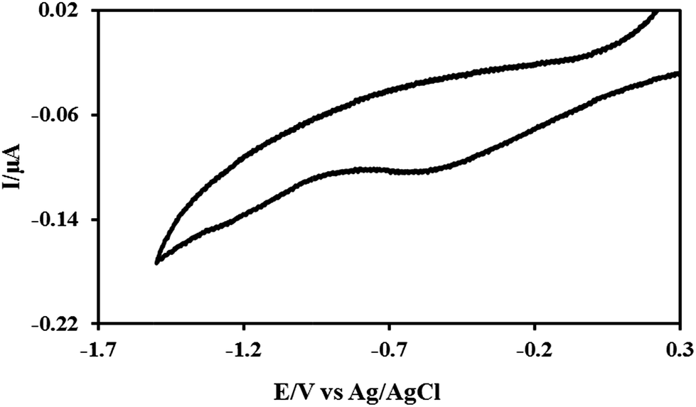 | ||
| Fig. 3 Cyclic voltammogram for an aqueous solution of calf thymus DNA and RhCl3·xH2O, supported upon n-doped Si 〈100〉 wafer, used as the working electrode. | ||
The as-prepared material was transferred to clean substrates for further analysis. As with the chemical reduction route, the XP survey scan spectrum of the nanostructures prepared by this electrochemical templating approach, Rh/DNAEchem, (ESI, Fig. S4†) indicated the presence of both DNA and rhodium the product. Peaks corresponding to Na1s and Cl2p, arising from the starting materials, are again also evident.
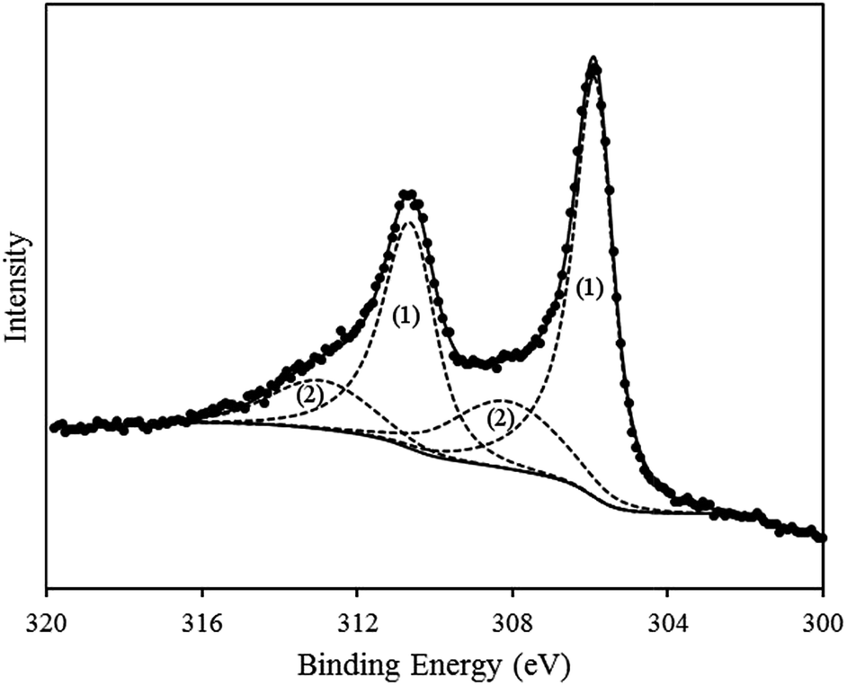
Confirmation that the metallic phase of Rh was deposited on the DNA templates was found in the Rh3d region of the spectrum. The corresponding Rh3d region of the XP data, again, indicated two different oxidation states (Fig. 4) assigned to zerovalent Rh0, formed upon electrochemical reduction and the presence of a Rh(III)-oxyhydroxide species, as for the Rh/DNAChem sample.65 The major component, with low-binding energies at 307.2 and 311.8 eV for 3d5/2 and 3d3/2 respectively, is in agreement with reported values of metallic Rh0.54,59,69–75 The higher BE doublet (3d5/2, 309.1 eV; 3d3/2, 313.5 eV) is again attributed to an oxidized species.73–75
 | ||
| Fig. 4 High resolution XPS spectrum of Rh3d region of DNA-templated Rh nanowires, prepared via the electrochemical reduction approach. The experimental data is shown (black dots), along with a curve fitting of the envelope (dashed lines). | ||
While both synthetic routes produce material with similar composition, i.e. metallic Rh0 core encapsulated by an oxidized sheath, comparison of the Rh3d region of the XPS spectra appears to reveal a ∼2-fold increase in the oxidized species for the electrochemically-prepared material. However, these nanowires are smaller (see Fig. 5) than those prepared by the chemical route and therefore in view of the surface-sensitivity of XPS the true extent of oxidation are not substantially different.
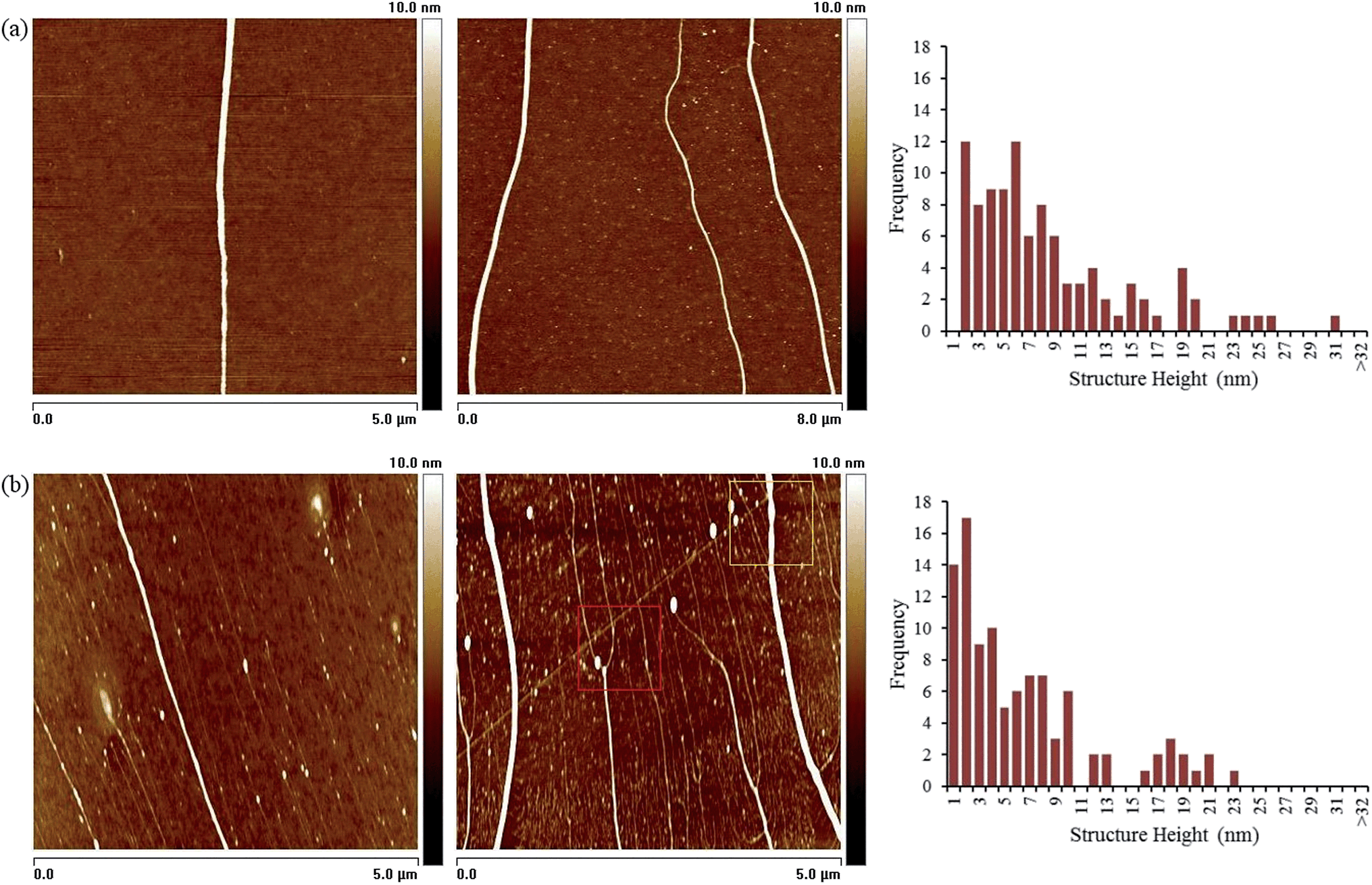 | ||
| Fig. 5 (a) AFM height images of DNA-templated Rh nanowires, prepared via the chemical reduction method, immobilised upon a Si/native SiO2 wafer, and a histogram showing the size (diameter) distribution of a sample of 100 nanowires. (b) AFM height images of DNA-templated Rh nanowires, prepared via the electrochemical reduction method, immobilised upon a Si/native SiO2 wafer, and a histogram showing the size (diameter) distribution of a sample of 100 nanowires. The nanowire diameters recorded in the histograms were determined from line profile measurements carried out using AFM data. | ||
Structural characterisation of Rh-nanowires
AFM was used to establish structural details of the prepared materials and to judge the effectiveness of DNA as a template to direct the growth of the metal. Samples suitable for imaging individual Rh nanostructures from both methods were prepared using molecular combing76,77 upon TMS-modified silicon/native oxide substrate. Fig. 5(a) shows AFM height images of some typical examples of the DNA-templated Rh nanostructures prepared via the chemical reduction method while Fig. 5(b) shows material from the electrochemical route.Analysis of material prepared in either case shows the structures to exhibit the high aspect-ratio of the template DNA molecules, but with larger diameter (bare DNA <2 nm by AFM, see S7 in ESI†).§ A statistical analysis (≥100 nanowires) of the heights of the structures, acquired from the AFM data, is also shown in Fig. 5. These data indicates a range of diameters from 3–31 nm, with a modal value of 6 nm from chemical reduction. This is rather larger than the value derived from the XRD data and indicates that the nanowires are comprised of particles smaller than the measured AFM diameter in a manner similar to our previously prepared DNA-templated Pd nanowires (ESI, Fig. S5†).78 A range of 3–23 nm with a modal value of 3–4 nm was found for the sample prepared by the electrochemical route.
Upon further inspection of the AFM data it can be seen that the Rh coatings along the length of the DNA appear to be continuous and rather regular. However, in some images a variety of morphologies is observed which include structures at an earlier stage of nanowire formation (e.g. see red and yellow boxes Fig. 5(b) and ESI Fig. S6†). These structures are identified as having a particles-on-a-string appearance, or display visible “necking”, features that are consistent with a growth of the nanowires taking place by a “nucleation and growth” mechanism. The uniform structure formation observed here has been attributed to a combination of instantaneous nucleation on the template (which favours uniform particle growth), and confinement of the nuclei to a 1D templates which results in inhibition of the growth of larger particles because they experience overlap with their neighbours sooner.50 Based on this, and the low temperature nature of the synthesis, the nanowires are expected to comprise closely packed particles. Comparison of the AFM and XRD data indicates that the morphology of these Rh nanowires has similarities to previously-published Pd nanowires;78 the crystallite size from XRD (2 nm) is too small to observe by microscopy and much less than the diameter of the nanowires. Pd and Rh are both noble metals and the reduction leads to the formation of many small nuclei in a highly irreversible process far from equilibrium. Lattice-gas simulations show that the external appearance of such nanowires may be rather smooth despite their complex internal structure.78
It is useful to make comparison of the two different approaches to preparing Rh-nanowires. While both produce examples of regular, smooth, continuous structures the effectiveness in terms of DNA metallisation of the electrochemical approach is comparatively low. Based on the statistical analysis, the fraction of bare DNA remaining with this method is considerably greater, by a factor of ∼3, than for the chemical reduction (note: structures with diameters ≤2 nm are judged to be DNA molecules which remain bare in the reaction solution79 (Fig. S7†), whereas thicker structures >2 nm are predominately DNA-templated Rh nanowires). This can be understood from the fact that the former method involves electron transfer at the electrode surface and thus a much smaller fraction of Rh(III) species are reduced than in the bulk solution chemical reduction method.
Electrical characterization
Characterisation of the electrical properties of the prepared Rh/DNA materials was performed in an effort to confirm their nanowire credentials using a combination of scanning probe microscopy (SPM) methods; specifically scanning conductance microscopy (SCM) and conductive AFM (cAFM). Initial investigations were carried out using SCM, as this provides a relatively simple means of rapidly establishing if such 1D nanostructures display electrical conductivity. These data, provided in the ESI,† indicate that the samples are electrically conducting (Fig. S8 and S9†).2,5Electrical characterisation was extended to conductive AFM (cAFM) which, though more technically challenging due to the need to make contact with the nanowires, provides more quantitative information. In addition, the ability to control the placement of the cAFM probe at specific points along the nanowire under investigation allows for distance-dependent measurements to be made. From this data the contribution to the nanowires resistance from the probe-nanostructure contact resistance can be extracted.
For these experiments we used our previously reported experimental method to perform these analyses.25 Briefly, this involves drop-casting nanowires from solution onto a Si/SiO2 substrate to form a large deposit of the nanostructured material.
At the periphery of the resulting deposit, it is possible (by AFM imaging) to identify individual, or small bundles of the, nanowires protruding from the larger network, (see ESI Fig. S10†). In this setup, the dense nanowire network can be exploited as a macroscopic electrode in contact with the end of the protruding nanowire to be studied. The conductive probe used in cAFM experiments is employed to act as the second electrode to make electrical contact with the nanowire.
Following acquisition of height/current data, an additional function of the cAFM mode was used to carry out i–V measurements in order to extract quantitative information regarding the nanowire's conductance. Here, the AFM probe was brought into contact at specific points along the length of the nanowire and i–V measurements recorded over the range of −5 V to +5 V. The nanowire resistance was subsequently estimated from the slope of the i–V curve around zero bias. It has previously been demonstrated that the information gathered in this manner can be used not only to determine the resistance per unit length of the nanowire, but also to extract the contribution to the measured resistance from the probe–nanowire contact resistance.25
Samples from both chemical and electrochemical reduction methods were investigated by these cAFM techniques and the results are shown in Fig. 6. From these data it was possible to calculate the resistance per unit length from the slope of the of best fit lines as; Rh-Chem = 2 × 10¹¹ Ω cm−1. Rh-Echem = 1 × 10¹¹ Ω cm−1. In order to estimate the nanowire conductivity, their diameter and width were determined by AFM in order to calculate the cross-section area (assumed elliptical). Based on these calculations, the conductivity of the DNA/Rh nanowires were Rh-Chem = 0.015 S cm−1; Rh-Echem = 0.024 S cm−1 and the resistivities Rh-Chem = 65 Ω cm; Rh-Echem = 41 Ω cm. The small difference in conductivity may relate to the mechanism of the reduction; electrochemically-prepared NWs consist of Rh particles formed by a faradaic process and therefore individual nuclei must be in some sort of electrical contact. In contrast, individual nuclei in the chemically-reduced NWs need not necessarily be in electrical contact with each other.
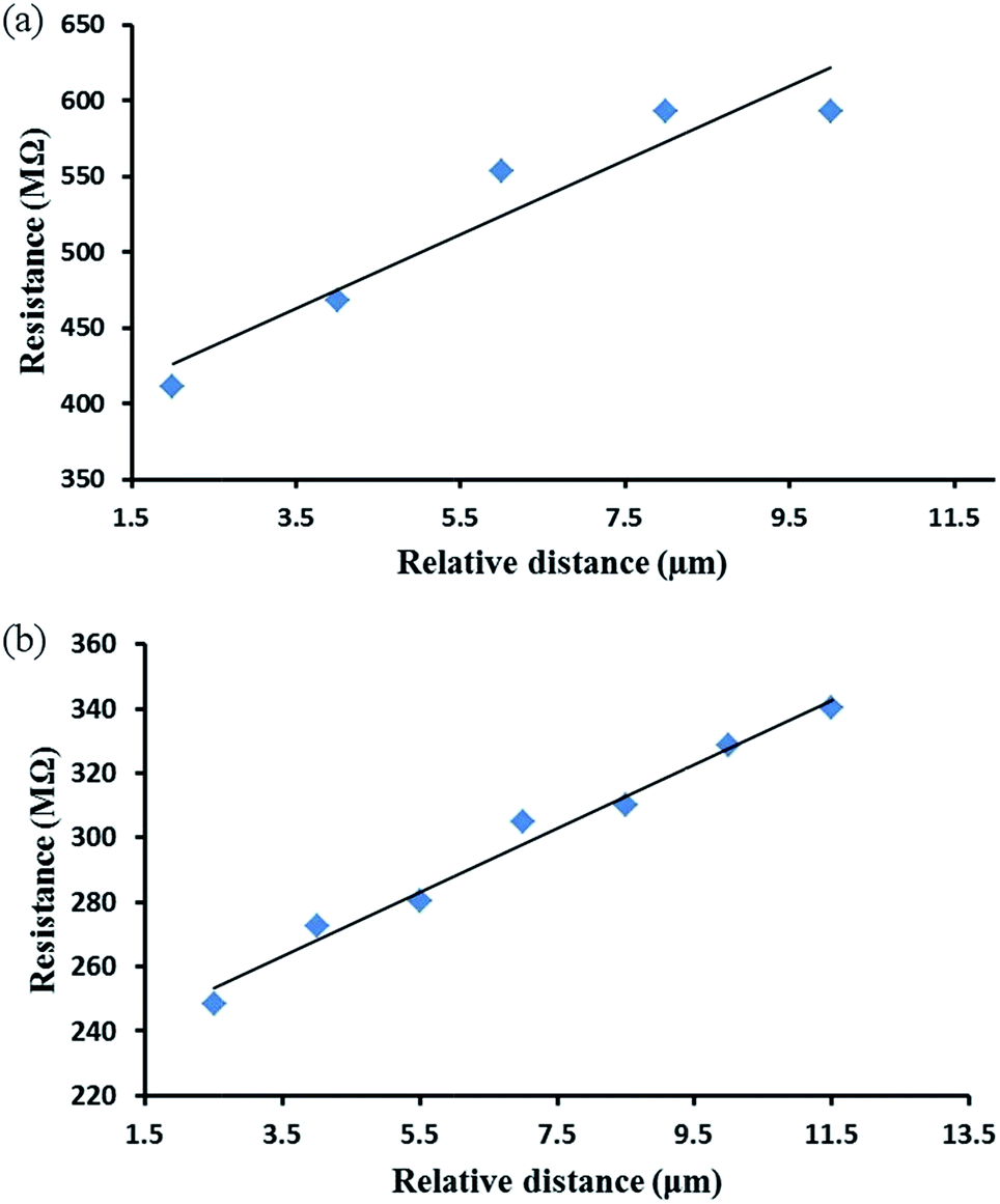 | ||
| Fig. 6 (a) Plot of the calculated resistance of a DNA-templated Rh nanowires prepared by chemical reduction as a function of relative distance. Each i–V measurement carried out to calculated the distance-dependent resistance, was performed at a deflection setpoint value of 0.5 V. (b) Resistance of electrochemically prepared DNA/Rh nanowires as a function of relative distance at deflection setpoint of 0.5 V. | ||
These resistivities are considerably greater than that reported for Rh in bulk form (4.7 × 10⁻⁶ Ω cm).80,81 Such increases in the material resistivity upon a reduction to the nanometre size regime are not uncommon, with the preparation of other metals in 1D nanoscale form showing increases in resistivity by several orders of magnitude.82–84 In the case of the Rh structures reported here, this increase in resistivity is suggested to be most likely the result of the granular character of the Rh coatings on the DNA strands, as indicated by AFM and XRD, and leading to electron scattering at particle–particle interfaces and the nanowire surface (note: resistance caused by surface scattering is expected to become increasingly significant as the diameter of the nanowire approaches and decreases below the bulk mean free path). There may also be a contribution from the formation of the oxyhydroxide layer on the nanowires surfaces, as indicated by the XPS data.
Conclusion
Rhodium nanowires have been successfully produced using DNA-templating in conjunction with either chemical or electrochemical reduction. The association of the metal cations with DNA templates directs the subsequent growth of the metallic Rh formed during the reduction step to give 1-D nanostructures. Chemical characterization of nanowires prepared using either method indicates these to comprise a metallic Rh0 core coated with oxidised Rh species. AFM studies indicated that both methods allow the fabrication of DNA/Rh nanowires with, essentially, complete coverage of the DNA templates by the Rh material. Closer inspection of the structures produced showed a degree of granular character associated with coatings, indicating that the metal growth upon the DNA template took place via a nucleation and growth mechanism.85 Despite the apparent granular nature of the nanowires investigation of electric conductivity indicates that the nanowires are conducting and hence the coating continuous. However their room temperature conductivity value, calculated from i–V curves recorded by c-AFM, was similar and low at 0.015 Scm−1 and 0.024 Scm−1, for chemical and electrochemical reduction, respectively. Based on the statistical analysis, the electrochemical method of preparation was less efficient, leaving a larger number of DNA molecules essentially bare. However, despite this, the simple demonstration of forming metal structures by an electrochemical method suggests the possibility for success of templating at more complex pre-assembled DNA-structures using high-resolution electrochemical techniques such as scanning electrochemical microscopy.Experimental
Materials
Rhodium(III) chloride hydrate (RhCl3·xH2O) (Rh 38.40%) and calf thymus DNA (CT-DNA) (highly polymerised, 6% sodium), were purchased from Sigma-Aldrich Company Ltd. (Gillingham, Dorset, UK) and used as received. Lambda DNA (λ-DNA, Cat. no. N3011S) was purchased from New England Biolabs UK Ltd. (Hitchin, Hertfordshire, UK). Sodium borohydride (NaBH4, 98%) was purchased from Alfa Aesar. Si 〈n-100〉 wafers (phosphorous doped, 525 ± 50 μm thickness, 1–10 Ω cm resistance, single side polished), were used as substrate supports for TappingMode™ AFM imaging. Si 〈n-100〉 wafers with a 200 nm thick, thermally grown SiO2 layer on top (arsenic doped, 500 ± 25 μm, <0.005 Ω cm resistance, thermal oxide layer 200 nm ± 10% thickness, double side polished) were used in scanned conductance microscopy and magnetic force microscopy experiments. All Si wafers were purchased from Compart Technology Ltd. (Peterborough, Cambridgeshire, UK). NANOpure® deionised water (18 MΩ cm resistivity) was obtained from a NANOpure® DIamondTM Life Science ultrapure water system equipped with a DIamondTM RO Reverse Osmosis System (Barnstead International).Large-scale preparation of DNA/Rh material using chemical reduction method
Samples for XRD and XPS studies were prepared through addition of 10 mL of an aqueous solution of RhCl3·xH2O (2.5 mM) to 5 mL of a solution of CT-DNA (500 μg mL−1). The mixture was left to stand for 10 days at room temperature, before adding a freshly prepared NaBH4 (10 mL; 25 mM) solution in water. The reaction solution turned brownish-black in colour and the resulting colloidal solution was then centrifuged and concentrated in order to extract the DNA/Rh final material. The collected black powder was allowed to dry at room temperature prior to analysis.Preparation of λ-DNA/Rh samples using chemical reduction method
5 μL of an aqueous solution of λ-DNA (500 μg mL−1) was mixed with 10 μL of an aqueous solution of RhCl3·xH2O (2.5 mM), and incubated for 10 days at room temperature. Then, a freshly prepared NaBH4 (10 μL; 25 mM) solution in water was added. The resulting DNA-templated rhodium nanostructures formed in the reaction solution was allowed to stand for further 10 min before being aligned on the TMS-modified Si 〈n-100〉 or Si〈n-100〉/200 nm SiO2 wafers for AFM and EFM measurements, respectively. For nanowires alignment, 5 μL of the DNA/Rh solution was applied to a TMS-modified wafer as previously described,26 whilst being spun at 125 rpm. The wafer was then spun for a further 2 minutes at 250 rpm before the residual solution was withdrawn from the surface by a micropipette. Finally, nanowires-modified wafer was left to dry at room temperature before performing scanning probe microscopy measurements.Large-scale preparation of DNA/Rh material using an electrochemical reduction method
40 μL of an aqueous solution of RhCl3·xH2O (2.5 mM) was mixed with 20 μL of an aqueous solution of CT-DNA (500 μg mL−1) and incubated at room temperature. Then, 40 μL of the reaction solution was applied to a chemically oxidized Si 〈n-100〉 substrate modified with a TMS SAM. The modified Si substrate was used as the working electrode during the electrochemical reduction process, while the counter and reference electrodes were a tungsten wire with diameter of 0.25 mm, and Ag/AgCl, respectively. The hydrophobic nature of the modified Si substrate results in ‘beading’ of the deposited DNA/Rh+3 solution enabling the counter and reference electrodes to be easily inserted into the solution droplet without contacting the substrate surface.Cyclic voltammetry measurements were performed using a computer-interfaced SECM CHI 900 electrochemical microscope system (CH Instruments, Austin, Texas, USA), sweeping the potential between E = 0.3 V and E = −0.3 V, with a scan rate of v = 0.1 V s−1, quiet time, t = 2.0 seconds, and sweep segments = 2.
After completion of the electrochemical reduction, the reaction solution was removed from the Si working electrode by micropipette and transferred to a fresh TMS-modified Si 〈p-100〉 substrate. The solvent was allowed to evaporating at room temperature in order to produce a thin film of the product materials for XPS analysis.
Preparation of λ-DNA/Rh samples using an electrochemical reduction method
For the AFM, EFM and MFM measurements, DNA/Rh samples were prepared using λ-DNA. Here, samples were prepared by mixing 10 μL of an aqueous solution of RhCl3·xH2O (2.5 mM) and 5 μL of an aqueous solution λ-DNA (500 μg mL−1). The resulting DNA/Rh3+ solution system was allowed to stand for 10 days at room temperature before performing any electrochemical reduction process. Cyclic voltammetry measurements were subsequently carried out upon a 5 μL of the DNA/Rh3+ solution system deposited on Si working electrode.Following the CV measurements, the resulting DNA/Rh nanowires in the reaction solution were transferred by micropipette into a new TMS-modified n-Si 〈100〉 wafer, and then aligned as described earlier.
FTIR studies
For FTIR studies, samples were prepared as films of material upon silicon substrates. Samples for DNA/Rh3+ were prepared by mixing an aqueous solution of CT-DNA (30 μL; 500 μg mL−1) with an aqueous solution of RhCl3·xH2O (30 μL; 2.5 mM). The resulting DNA/Rh3+ solution were allowed to stand at room temperature for 20 minutes. After 20 minutes reaction time had elapsed, 80 μL of the reaction solution was deposited upon a silicon substrate, and allowing the solvent to evaporate at room temperature. Samples of bare DNA were prepared by depositing 80 μL of a CT-DNA solution (500 μg mL−1) upon Si substrates and the solvent allowed to evaporate at room temperature. FTIR spectra were performed with a Bio-Rad Excalibur FTS-40 spectrometer (Varian Inc., Palo Alto, CA, USA), and spectra were recorded over the 400–4000 cm−1 range, with 128 scans and at 4 cm−1 resolution.Powder X-ray diffraction
Samples of DNA/Rh material were prepared for powder X-ray diffraction (XRD) analysis by drop-casting the reaction solution onto piranha-cleaned Si 〈n-100〉 wafer and allowing to dry at room temperature. A PAN-alytical X'Pert Pro diffractometer equipped with a Cu Kα radiation source (λ = 1.540 Å) was used for powder XRD data collection.X-ray photoelectron spectroscopy (XPS)
XPS analysis was carried out using a Thermo K-Alpha XPS system with a monochromated Al Kα X-ray source. An electron/ion gun was used to compensate for charge build-up on the sample during analysis, and all binding energies were referenced to the C1s hydrocarbon peak at 284.6 eV.Scanning probe microscopy
TappingMode™ AFM imaging was performed in air, using Multimode Nanoscope IIIa and Dimension Nanoscope V instruments (Veeco Instruments Inc., Metrology Group, Santa Barbara, CA), with TESP (n-doped Si cantilevers, resonant frequency = 230–410 kHz, spring force constant = 20–80 N m−1 Veeco Instruments Inc.), and Tap300Al-G (Si cantilevers, resonant frequency = 200–400 kHz, spring force constant = 20–75 N m−1, BudgetSensors) probes. Data acquisition was carried out using Nanoscope software version 5.12b36 (Multimode) and Nanoscope software version 7.00b19 (Dimension Nanoscope V) (Veeco Instruments Inc., Digital Instruments). For both AFM systems, vibrational noise was reduced with an isolation table (Veeco Inc., Metrology Group).Scanning conductance microscopy (SCM) was performed in air, on a Dimension Nanoscope V system, using MESP probes (n-doped Si cantilevers, metallic Co/Cr coating, resonant frequency = 50–100 kHz, spring force constant = 1–5 N m−1, Veeco Instruments Inc.). Data acquisition was carried out using Nanoscope version 7.00b19 software.
Conductive AFM (cAFM) experiments were performed on a Dimension Nanoscope V AFM, using MESP probes. Both topographical data (obtained in contact mode) and current maps were acquired simultaneously during cAFM operation. Samples for analysis were prepared as previously described.25
Acknowledgements
X-ray photoelectron spectra were obtained at the National EPSRC XPS User's Service (NEXUS) at Newcastle University, an EPSRC mid-range facility. This work was financially supported by One North East, EU-FP7 project LAMAND (Contract no. 245565), EU ITN NANOEMBRACE (Contract no. 316751), Newcastle University, Azzaytuna University, Tarhuna, Libya, and the Libyan Government.Notes and references
- R. J. Gehr and R. W. Boyd, Chem. Mater., 1996, 8, 1807–1819 CrossRef CAS.
- U. Heiz and W. D. Schneider, Crit. Rev. Solid State Mater. Sci., 2001, 26, 251–290 CrossRef CAS.
- G. Li and R. Jin, Acc. Chem. Res., 2013, 46, 1749–1758 CrossRef CAS PubMed.
- B. Lim and Y. Xia, Angew. Chem., Int. Ed., 2011, 50, 76–85 CrossRef CAS PubMed.
- P. Moriarty, Rep. Prog. Phys., 2001, 64, 297–381 CrossRef CAS.
- T. Nagao, G. Han, C. Hoang, J. S. Wi, A. Pucci, D. Weber, F. Neubrech, V. M. Silkin, D. Enders, O. Saito and M. Rana, Sci. Technol. Adv. Mater., 2010, 11, 054506 CrossRef.
- H. F. Qian, M. Z. Zhu, Z. K. Wu and R. C. Jin, Acc. Chem. Res., 2012, 45, 1470–1479 CrossRef CAS PubMed.
- N. S. Ramgir, Y. Yang and M. Zacharias, Small, 2010, 6, 1705–1722 CrossRef CAS PubMed.
- J. Sharma and T. Imae, J. Nanosci. Nanotechnol., 2009, 9, 19–40 CrossRef CAS PubMed.
- I. Dıez and R. H. A. Ras, Nanoscale, 2011, 3, 1963–1970 RSC.
- P. K. Jain, X. Huang, I. H. El-Sayed and M. A. El-Sayed, Acc. Chem. Res., 2008, 41, 1578–1586 CrossRef CAS PubMed.
- G. J. Hutchings and C. J. Kiely, Acc. Chem. Res., 2013, 46, 1759–1772 CrossRef CAS PubMed.
- L. L. Chng, N. Erathodiyil and J. Y. Ying, Acc. Chem. Res., 2013, 46, 1825–1837 CrossRef CAS PubMed.
- S. Schauermann, N. Nilius, S. Shaikhutdinov and H.-J. Freund, Acc. Chem. Res., 2012, 46, 1673–1681 CrossRef PubMed.
- H. Zhang, M. Jin, Y. Xiong, B. Lim and Y. Xia, Acc. Chem. Res., 2013, 46, 1783–1794 CrossRef CAS PubMed.
- C. M. Leiber, MRS Bull., 2003, 28, 486–491 CrossRef.
- Y. Yuan, N. Yan and P. J. Dyson, ACS Catal., 2012, 2, 1057–1069 CrossRef CAS.
- B. R. Sathe, B. K. Balan and V. K. Pillai, Energy Environ. Sci., 2011, 4, 1029–1035 CAS.
- D. A. Boyd, Y. Hao, C. Li, D. G. Goodwin and S. M. Haile, ACS Nano, 2013, 7, 4919–4923 CrossRef CAS PubMed.
- M. Li, T. S. Mayer, J. A. Sioss, C. D. Keating and R. B. Bhiladvala, Nano Lett., 2007, 7, 3281–3284 CrossRef CAS PubMed.
- M. Zahmakiran, Y. Román-Leshkov and Y. Zhang, Langmuir, 2012, 28, 60–64 CrossRef PubMed.
- L. Dong, T. Hollis, B. A. Connolly, N. G. Wright, B. R. Horrocks and A. Houlton, Adv. Mater., 2007, 19, 1748–1751 CrossRef CAS.
- L. Dong, T. Hollis, S. Fishwick, B. A. Connolly, N. G. Wright, B. R. Horrocks and A. Houlton, Chem.–Eur. J., 2007, 13, 822–828 CrossRef CAS PubMed.
- J. Hannant, J. H. Hedley, J. Pate, A. Walli, S. A. Farha Al-Said, M. A. Galindo, B. A. Connolly, B. R. Horrocks, A. Houlton and A. R. Pike, Chem. Commun., 2010, 46, 5870–5872 RSC.
- R. Hassanien, M. Al-Hinai, S. A. Farha Al-Said, R. Little, L. Šiller, N. G. Wright, A. Houlton and B. R. Horrocks, ACS Nano, 2010, 4, 2149–2159 CrossRef CAS PubMed.
- R. Hassanien, S. A. Farha Al-Said, L. Šiller, R. Little, N. G. Wright, A. Houlton and B. R. Horrocks, Nanotechnology, 2012, 23, 075601 CrossRef PubMed.
- Y. Ma, J. Zhang, G. Zhang and H. He, J. Am. Chem. Soc., 2004, 126, 7097–7101 CrossRef CAS PubMed.
- H. D. A. Mohamed, S. M. D. Watson, B. R. Horrocks and A. Houlton, Nanoscale, 2012, 4, 5936–5945 RSC.
- S. Pruneanu, S. A. Farha Al-Said, L. Dong, T. A. Hollis, M. A. Galindo, N. G. Wright, A. Houlton and B. R. Horrocks, Adv. Funct. Mater., 2008, 18, 2444–2454 CrossRef CAS.
- S. M. D. Watson, J. H. Hedley, M. A. Galindo, S. A. Farha Al-Said, N. G. Wright, B. A. Connolly, B. R. Horrocks and A. Houlton, Chem.–Eur. J., 2012, 18, 12008–12019 CrossRef CAS PubMed.
- A. Houlton, A. R. Pike, M. A. Galindo and B. R. Horrocks, Chem. Commun., 2009, 1797–1806 RSC.
- A. Houlton and S. M. D. Watson, Annu. Rep. Prog. Chem., Sect. A: Inorg. Chem., 2011, 107, 21–42 RSC.
- Y. Geng, A. C. Pearson, E. P. Gates, B. Uprety, R. C. Davis, J. N. Harb and A. T. Woolley, Langmuir, 2013, 29, 3482–3490 CrossRef CAS PubMed.
- P. W. K. Rothemund, Nature, 2006, 440, 297 CrossRef CAS PubMed.
- D. Borissov, S. Isik-Uppenkamp and M. Rohwerder, J. Phys. Chem. C, 2009, 113, 3133–3138 CAS.
- M.-M. Song, W.-J. Song, H. Bi, J. Wang, W.-L. Wu, J. Sun and M. Yu, Biomaterials, 2010, 31, 1509–1517 CrossRef CAS PubMed.
- Q. Wang, G. Wang, B. Xu, J. Jie, X. Han, G. Li, Q. Li and J. G. Hou, Mater. Lett., 2005, 59, 1378–1382 CrossRef CAS PubMed.
- J. Verbeeck, O. I. Lebedev, G. Van Tendeloo, L. Cagnon, C. Bougerol and G. Tourillon, J. Electrochem. Soc., 2003, 150, E468–E471 CrossRef CAS PubMed.
- D. Wang, H. P. Jakobson, R. Kou, J. Tang, R. Z. Fineman, D. Yu and Y. Lu, Chem. Mater., 2006, 18, 4231–4237 CrossRef CAS.
- D. Wang, H. Luo, R. Kou, M. P. Gil, S. Xiao, V. O. Golub, Z. Yang, C. J. Brinker and Y. Lu, Angew. Chem., Int. Ed., 2004, 43, 6169–6173 CrossRef CAS PubMed.
- W. E. Ford, O. Harnack, A. Yasuda and J. M. Wessels, Adv. Mater., 2001, 13, 1793–1797 CrossRef CAS.
- K. Keren, R. S. Berman and E. Braun, Nano Lett., 2004, 4, 323–326 CrossRef CAS.
- K. Keren, M. Krueger, R. Gilad, G. Ben-Yoseph, U. Sivan and E. Braun, Science, 2002, 297, 72–75 CrossRef CAS PubMed.
- E. Braun, Y. Eichen, U. Sivan and G. Ben-Yoseph, Nature, 1998, 391, 775–778 CrossRef CAS PubMed.
- J. Richter, M. Mertig, W. Pompe, I. Mönch and H. K. Schackert, Appl. Phys. Lett., 2001, 78, 536–538 CrossRef CAS PubMed.
- J. Richter, R. Seidel, R. Kirsch, M. Mertig, W. Pompe, J. Plaschke and H. K. Schackert, Adv. Mater., 2000, 12, 507–510 CrossRef CAS.
- C. F. Monson and A. T. Woolley, Nano Lett., 2003, 3, 359–363 CrossRef CAS.
- S. M. D. Watson, N. G. Wright, B. R. Horrocks and A. Houlton, Langmuir, 2010, 26, 2068–2075 CrossRef CAS PubMed.
- Q. Gu, C. Cheng and D. T. Haynie, Nanotechnology, 2005, 16, 1358–1363 CrossRef CAS.
- S. M. D. Watson, H. D. A. Mohamed, B. R. Horrocks and A. Houlton, Nanoscale, 2013, 5, 5349–5359 RSC.
- J. Lui, B. Uprety, S. Gyawali, A. T. Woolley, N. V. Myung and J. N. Harb, Langmuir, 2013, 29, 11176–11184 CrossRef PubMed.
- Nucleic Acid - Metal Ion Interactions, Ed. T. Spiro, in Metal Ions in Biology Series, Vol. 1, John Wiley & Sons, New York, 1980 Search PubMed.
- G. L. Eichhorn and Y. A. Shin, J. Am. Chem. Soc., 1968, 90, 7323–7328 CrossRef CAS.
- H.-B. Pan and C. M. Wai, J. Phys. Chem. C, 2010, 114, 11364–11369 CAS.
- Y. T. Jeon and G. H. Lee, J. Appl. Phys., 2008, 103, 094313/094311–094313/094315 CrossRef PubMed.
- K. S. Lokesh, Y. Shivaraj, B. P. Dayananda and S. Chandra, Bioelectrochemistry, 2009, 75, 104–109 CrossRef CAS PubMed.
- J. D. Hoefelmeyer, K. Niesz, G. A. Somorjai and T. D. Tilley, Nano Lett., 2005, 5, 435–438 CrossRef CAS PubMed.
- T. D. Ewers, A. K. Sra, B. C. Norris, R. E. Cable, C.-H. Cheng, D. F. Shantz and R. E. Schaak, Chem. Mater., 2005, 17, 514–520 CrossRef CAS.
- Y. Zhang, M. E. Grass, S. E. Habas, F. Tao, T. Zhang, P. Yang and A. Somorjai, J. Phys. Chem. C, 2007, 111, 12243–12253 CAS.
- E. W. Nuffield, X-Ray Diffraction Methods, Wiley, New York, 1966 Search PubMed.
- Y. Baer, P. F. Heden, J. Hedman, M. Klasson, C. Nordling and K. Siegbahn, Phys. Scr., 1970, 1, 55 CrossRef CAS.
- A. M. Dennis, R. A. Howard, K. M. Kadish, J. L. Bean, J. Brace and N. Winograd, Inorg. Chim. Acta, 1980, 44, L139 CrossRef CAS.
- N. Claessens, F. Demoisson, T. Dufour, A. Mansour, A. Felten, J. Guillot, J.-J. Pireaux and F. Reniers, Nanotechnology, 2010, 21, 385603 CrossRef CAS PubMed.
- Y. Okamoto, N. Ishida, T. Imanaka and S. Teranishi, J. Catal., 1979, 58, 82 CrossRef CAS.
- F. A. Cotton, G. Wilkinson, C. A. Murillo and M. Bochman, Advanced Inorganic Chemistry, Wiley Interscience, USA, 1999 Search PubMed.
- Y. Zhang, M. E. Grass, S. E. Habas, F. Tao, T. Zhang, P. Yang and G. A. Somorjai, J. Phys. Chem. C, 2007, 111, 12243–12253 CAS.
- Y. Abe, K. Kato, M. Kawamura and K. Sasaki, Surf. Sci. Spectra, 2001, 8, 117 CrossRef CAS.
- J. Wang and Z. Taha, Talanta, 1991, 38, 489–492 CrossRef CAS.
- V. Cimpeanu, M. Kočevar, V. I. Parvulescu and W. Leitner, Angew. Chem., Int. Ed., 2009, 48, 1085–1088 CrossRef CAS PubMed.
- J. P. Contour, G. Mouvier, M. Hoogewys and C. Leclere, J. Catal., 1977, 48, 217–228 CrossRef CAS.
- R. Nyholm and N. Mårtensson, J. Phys. C: Solid State Phys., 1980, 13, L279–L284 CrossRef CAS.
- C. Force, E. Román, J. M. Guil and J. Sanz, Langmuir, 2007, 23, 4569–4574 CrossRef CAS PubMed.
- G. Gallaher, J. G. Goodwin Jr, C.-S. Huang and M. Houalla, J. Catal., 1991, 127, 719–731 CrossRef CAS.
- C. Sleigh, A. P. Pijpers, A. Jaspers, B. Coussens and R. J. Meier, J. Electron Spectrosc. Relat. Phenom., 1996, 77, 41–57 CrossRef CAS.
- J. P. Contour, G. Mouvier, M. Hoogewys and C. Leclere, J. Catal., 1977, 48, 217–228 CrossRef CAS.
- J. Li, C. Bai, C. Wang, C. Zhu, Z. Lin, Q. Li and E. Cao, Nucleic Acids Res., 1998, 26, 4785–4786 CrossRef CAS PubMed.
- Z. Deng and C. Mao, Nano Lett., 2003, 3, 1545–1548 CrossRef CAS.
- M. N. Al-Hinai, R. Hassanien, N. G. Wright, A. B. Horsfall, A. Houlton and B. R. Horrocks, Faraday Discuss., 2013, 164, 71–91 RSC.
- S. M. D. Watson, J. H. Hedley, M. A. Galindo, S. A. F. Al-Said, N. G. Wright, B. A. Connolly, B. R. Horrocks and A. Houlton, Chem.–Eur. J., 2012, 18, 12008–12019 CrossRef CAS PubMed.
- G. K. White and S. B. Woods, Philos. Trans. R. Soc., A, 1959, 251, 273–302 CrossRef.
- E. Y. Garcia and D. G. Loffler, J. Chem. Eng. Data, 1985, 30, 304–305 CrossRef CAS.
- K. Critchley, B. P. Khanal, M. L. Gorzny, L. Vigderman, S. D. Evans, E. R. Zubarev and N. A. Kotov, Adv. Mater., 2010, 22, 2338–2342 CrossRef CAS PubMed.
- A. Bid, A. Bora and A. K. Raychaudhuri, Phys. Rev. B: Condens. Matter Mater. Phys., 2006, 74, 035426 CrossRef.
- J. Pate, F. Zamora, S. M. D. Watson, N. G. Wright, B. R. Horrocks and A. Houlton, J. Mater. Chem. C, 2014, 2, 9265–9273 RSC.
- S. M. D. Watson, A. Houlton and B. R. Horrocks, Nanotechnology, 2014, 23, 505603 CrossRef PubMed.
Footnotes |
| † Electronic supplementary information (ESI) available: FTIR data and assignments, P-XRD fit, XPS, scheme, AFM, SCM and cAFM data. See DOI: 10.1039/c4tc02307b |
| ‡ Current address: Chemistry Department, Faculty of Arts and Science, Azzaytuna University, P.O. Box 39011/39010, Tarhuna, Libya. |
| § The theoretical diameter of a molecule of duplex DNA is 2 nm, though AFM is well-known to underestimate this size (likely due to tip-induced compression of the molecule), with values as low as <1.0 nm commonly measured. |
| This journal is © The Royal Society of Chemistry 2015 |