
 Open Access Article
 This Open Access Article is licensed under a
 Creative Commons Attribution 3.0 Unported Licence
Exploring high temperature templating in non-planar phthalocyanine/copper iodide (111) bilayers†
Alexandra J.
Ramadan‡
a,
Luke A.
Rochford‡
*b,
Dean S.
Keeble‡
c,
Paul
Sullivan‡
b,
Mary P.
Ryan‡
a,
Tim S.
Jones‡
b and
Sandrine
Heutz‡
a
aDepartment of Materials, Imperial College London, Exhibition Road, London, SW7 2AZ, UK
bDepartment of Chemistry, University of Warwick, Gibbet Hill Road, Coventry, CV4 7AL, UK. E-mail: luke.rochford@warwick.ac.uk; Tel: +44 (0)2476522543
cDepartment of Physics, University of Warwick, Gibbet Hill Road, Coventry, CV4 7AL, UK
First published on 14th November 2014
Abstract
Elevated substrate temperature growth of phthalocyanine thin films is known to influence film morphology and increase crystallinity. Structural templating offers another method through which the structure of phthalocyanine films can be controlled. Here we combine the use of copper iodide (CuI) and elevated substrate temperatures and investigate their effect on the growth of a non-planar phthalocyanine system. Employing X-ray diffraction and atomic force microscopy we present detailed surface and crystal structure information. Vanadyl phthalocyanine (VOPc) is shown to adopt an edge-on orientation on CuI at ambient substrate temperatures, a behaviour in stark contrast to that of previously studied planar phthalocyanine molecules. Elevated substrate temperature is shown to result in changes in the surface morphology and structure demonstrating the versatility of the system. The crystal structure of VOPc was redetermined and used to infer the molecular orientation of the various VOPc/CuI bilayer structures.
Introduction
The morphology and crystal structure of organic semiconductor thin films impact directly on their physical properties.1–3 Precise control of the growth of organic semiconductors is of the utmost importance as it enables these characteristics to be tuned for specific applications including organic photovoltaic (OPV) and thin film transistor (OTFT) devices.4,5 One of the most widely studied classes of organic semiconductors is the metallophthalocyanine (MPc) family of molecules. These are widely used in small molecule OPV devices due to their ease of synthesis, chemical stability and compatibility with vacuum evaporation.6 The intermolecular distances and molecular orientation in crystalline MPcs have been shown to impact charge transport in thin films and single crystals.7–9 In order to exploit this anisotropy through structure control, thin organic or inorganic template layers have been utilized to enhance device parameters.1,4,10 One prominent example is the use of copper(I) iodide (CuI) as an interlayer between a transparent indium tin oxide (ITO) electrode and an MPc active layer to modify the molecular orientation therein.11 The effect of CuI on MPc films has also been studied in OPV devices resulting in an improvement in efficiency due to enhanced transport and optical properties which have been modelled using theoretical simulations.10,12 An additional route to achieving morphological control is growth employing elevated substrate temperatures, which significantly increases the crystal size in organic thin films and impacts upon device performance by increasing crystal size and therefore improving charge transport.13–15 Although the effects of structural templating and heated deposition on organic films are independently well established, the effects of their combination have received very little attention. Planar MPcs have been the main focus of investigations concerning the structural templating effects of CuI, motivated by their widespread use in efficient OPV devices.10,16 Non-planar MPcs exhibit some unique advantages over their planar counterparts including broader optical absorption profiles and shifted frontier energy level positions.17,18 These properties have led to their use in efficient OPV and OTFT devices although far less fundamental characterization data is present in the literature.19–21 Of the non-planar MPcs the effects of CuI have only been studied in lead phthalocyanine (PbPc) thin films.12 Many MPcs possess a single metal atom in the central imidazole cavity and in the case of PbPc it is the large atomic radius of the Pb atom (which sits above the molecular plane) that results in its non-planar nature. Vanadyl phthalocyanine (VOPc), which is also non-planar, is fundamentally different from PbPc since the oxo-vanadium moiety lies orthogonal to the molecular plane.22 A permanent dipole is present along the V![[double bond, length as m-dash]](https://www.rsc.org/images/entities/char_e001.gif) O bond, a feature not possessed by any of the planar MPcs. In this work we report the preparation and characterization of evaporated thin films of VOPc and VOPc/CuI bilayers. Films of VOPc and CuI have been deposited at both ambient and elevated substrate temperature, and the effect of CuI templating on VOPc films deposited in both conditions is shown. Surprisingly the use of a CuI interlayer results in the presence of diffraction planes corresponding to a molecular orientation normal to the substrate. This is in direct contrast to the behaviour normally observed for planar MPcs. Control of both molecular orientation and grain size in VOPc films is demonstrated using the combination of substrate temperature and the nature of the substrate. Furthermore the single crystal structure of VOPc is redetermined to ensure accurate assignment of the thin film structure.
O bond, a feature not possessed by any of the planar MPcs. In this work we report the preparation and characterization of evaporated thin films of VOPc and VOPc/CuI bilayers. Films of VOPc and CuI have been deposited at both ambient and elevated substrate temperature, and the effect of CuI templating on VOPc films deposited in both conditions is shown. Surprisingly the use of a CuI interlayer results in the presence of diffraction planes corresponding to a molecular orientation normal to the substrate. This is in direct contrast to the behaviour normally observed for planar MPcs. Control of both molecular orientation and grain size in VOPc films is demonstrated using the combination of substrate temperature and the nature of the substrate. Furthermore the single crystal structure of VOPc is redetermined to ensure accurate assignment of the thin film structure.
Experimental
Copper iodide (Sigma Aldrich, UK) was used as received and evaporated from a home built evaporator at 310 °C at a rate of 0.5 Å s−1 as measured by a calibrated quartz crystal microbalance. VOPc (Acros Organics, BE) was triply purified by thermal gradient sublimation23 and the resulting crystals were used for growth from a home built evaporator at 370 °C at a rate of 0.3 Å s−1. All films were grown in a custom built ultra-high vacuum (UHV) chamber with a base pressure of 3 × 10⁻⁹ mbar in which inorganic and organic materials were sublimed onto ambient and elevated temperature substrates. The substrate temperature was measured using a K-type thermocouple mounted close to the sample and calibrated using an optical pyrometer. Substrates were 10 × 10 mm pieces of thermally oxidized silicon (100) single crystal (IDB technologies, UK) cleaned in Decon-90®/de-ionized water mix, acetone and isopropanol. These were dried in a stream of dry nitrogen and cleaned by UV-ozone before being loaded into vacuum. Crystals for single crystal X-ray diffraction (XRD) measurements were grown using a home-built thermal gradient sublimation apparatus with a base pressure of 2 × 10⁻⁷ mbar. The crystal was attached to a glass fiber with Fomblin oil; this in turn was mounted in a goniometer head on an Oxford Diffraction Gemini diffractometer at 150 K, equipped with a Ruby CCD area detector, and held at 150 K during data collection. Refinements were carried out in Olex2 using the ShelX refinement algorithms.24,25 Thin film XRD patterns and pole figures were obtained using a PANalytical X'Pert Pro MRD diffractometer with monochromatic Cu Kα1 radiation. Powder XRD patterns were obtained using a PANalytical X'Pert Pro MPD diffractometer with monochromatic CuKα1 radiation. Atomic force microscopy (AFM) images were recorded using an Asylum research MFP-3D in AC mode (tapping mode) using Olympus AC240-TS silicon tips. Rietveld refinement was carried out in Topas Academic V4.26Results
Our previous work has demonstrated that it is the (111) surface present in polycrystalline CuI thin films which is responsible for its templating effects.16 For this reason the behaviour of VOPc has been investigated solely on films predominantly composed of (111) surfaces.Thin films of CuI (30 nm) were grown at ambient and elevated substrate temperatures using the methodology reported previously and described in the experimental section.16 X-ray diffraction (XRD) patterns of CuI films grown at ambient substrate temperature (Fig. S1†) exhibit a single broad peak at 2θ = 25.5° corresponding to the (111) lattice spacing of CuI (ICSD no. 23990). Atomic force microscopy (AFM) was used to investigate the morphology of the films which were found to be polycrystalline with a low surface roughness (Rq) of 0.7 nm (Fig. S1†). When CuI films were grown at an elevated substrate temperature (155 °C) only {111}-type reflections were observed in XRD patterns (Fig. 1). These films were found to have higher roughness (Rq = 6.3 nm) than their ambient counterparts with significantly larger grains seen in AFM topography images. X-ray pole figure analysis (Fig. S2†) was carried out on the CuI (111) reflection and confirms the high degree of orientation of the films out of the substrate plane. The in-plane orientation of the grains has a large mosaic spread (consistent with the AFM images) as was expected due to the amorphous surface of the SiO2 substrate.
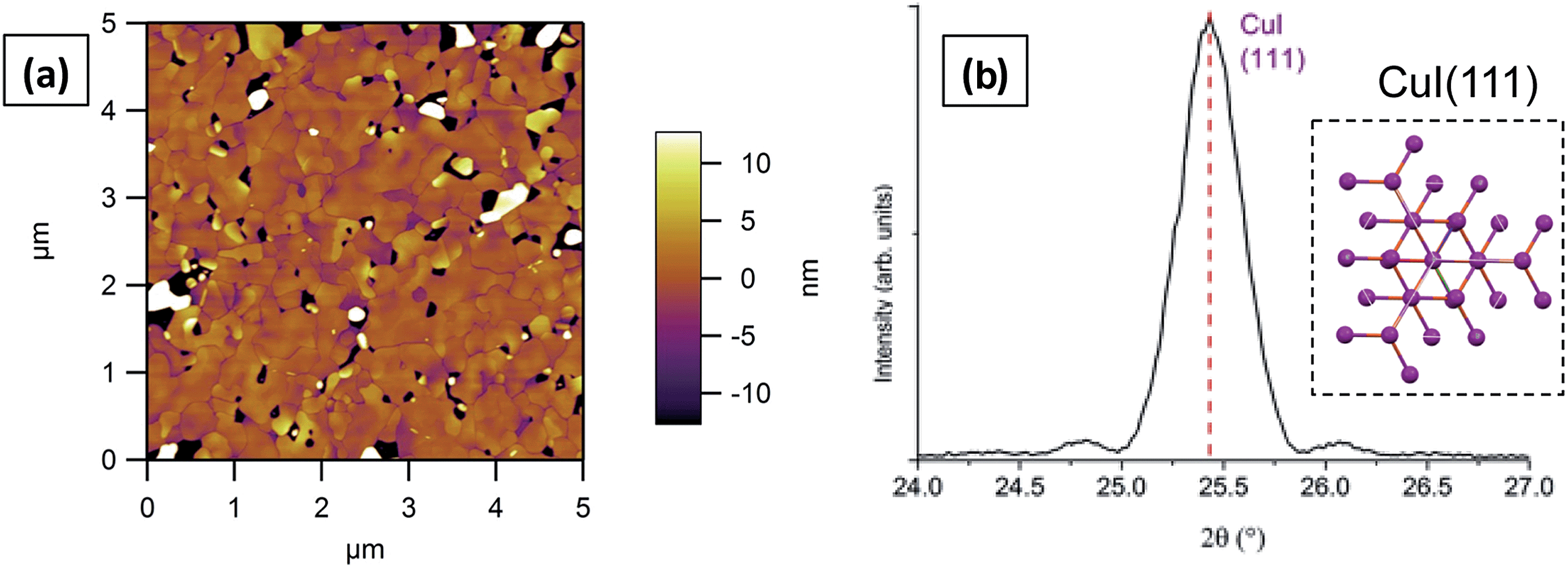 | ||
| Fig. 1 (a) AFM topography image and (b) XRD pattern of a 30 nm film of CuI grown on SiO2 at 155 °C. Inset of (b) shows a representation of the view orthogonal to the CuI (111) plane. | ||
Sequential growth of VOPc on the CuI (111) films was carried out in vacuo without exposure to air at ambient substrate temperature or at 155 °C. The VOPc films grown at ambient substrate temperatures (Tsub = 25 °C) exhibit uniform growth, relatively low surface roughness (Rq = 3.6 nm) and are composed of small grains of VOPc (Fig. 2). The morphology of these films is similar to that of VOPc grown at ambient substrate temperature on bare SiO2 (Fig. S3†). Despite the similarity in morphology changes in the molecular orientation within crystallites were revealed using X-ray diffraction (XRD). Thin films of VOPc/SiO2 grown at ambient substrate temperature result in featureless XRD patterns (Fig. S3a†) whereas the equivalent VOPc layer grown on CuI is characterized by a peak at 2θ = 26.2° (Fig. 2). This previously unseen peak indicates that the CuI layer modifies the growth of VOPc. The films grown at elevated substrate temperatures possess very different morphology to that of any of the samples previously discussed. On SiO2, the VOPc film is composed of grains with a triangular habit in AFM images (Fig. S3†). In contrast the AFM images of VOPc/CuI films show rectangular grains, the largest of which is 2 μm in length, surrounded by smaller more circular features (Fig. 2d). High growth temperature VOPc/CuI films exhibit much higher surface roughness (Rq = 23 nm) when compared with identical films grown at room temperature (Rq = 3.6 nm). The change in morphology is accompanied by a change in the XRD patterns of these films, suggesting either a change in structure, or a change in the distribution of orientations. VOPc grown on bare SiO2 at elevated substrate temperature (Fig. S3†) is characterized by two peaks at 2θ = 7.6° and 28.6°. Patterns of the VOPc grown on CuI are different and show three peaks corresponding to the VOPc layer (at 2θ = 12.9°, 26.2° and 28.6°), with the low angle peak previously unreported in films of VOPc grown on any substrate.
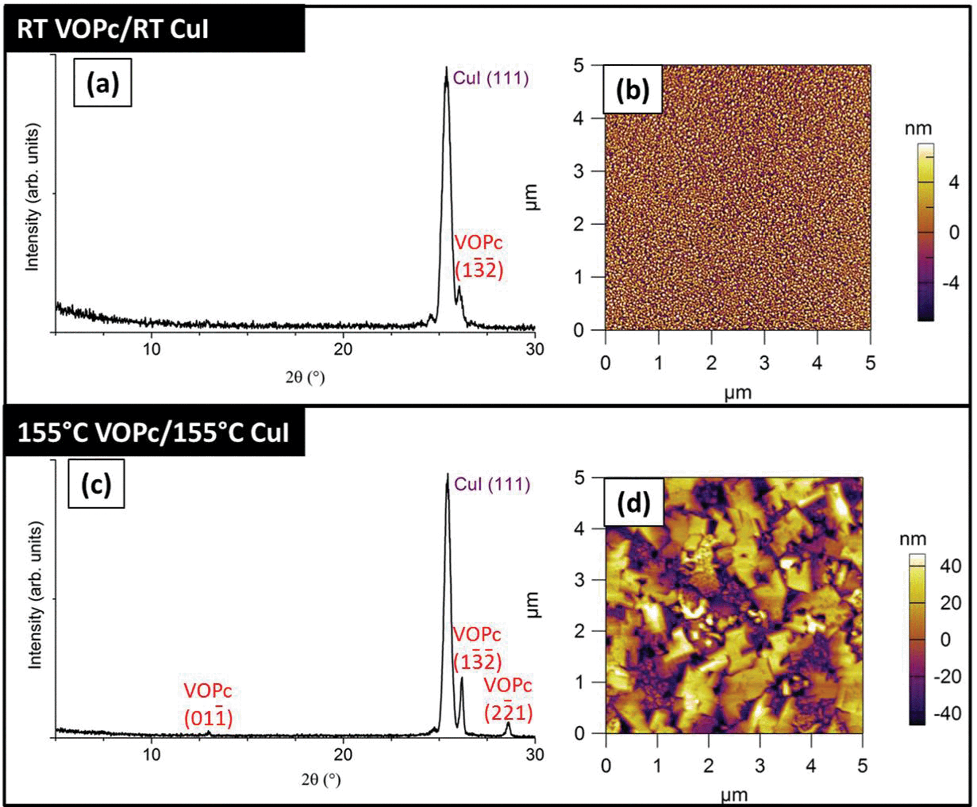 | ||
| Fig. 2 (a) XRD pattern and (b) AFM image of 50 nm VOPc grown on CuI/SiO2 film at ambient substrate temperature. (c) XRD pattern and (d) AFM image of 50 nm VOPc grown on CuI/SiO2 at 155 °C. | ||
A high-quality crystal structure was required to ensure an accurate assignment of Miller indices to the Bragg reflections observed in the diffraction experiments. Block-like single crystals of VOPc were grown using thermal gradient sublimation, the largest of which (100 × 50 × 50 μm) was used for single-crystal XRD experiments. The resulting single crystal structure (CCDC no. 1017243†) is very similar to the previously published VOPc single crystal structure data.27 Current convention dictates that the cell be indexed using the reduced cell, in contrast to the convention used when the previous structure was solved. The redetermined structure has an improved R factor and there are slight changes in some of the C–H bond angles and lattice spacings. A summary and representation of the two structures is shown in Fig. 3, and complete structural information can be obtained from the CCDC. Using this crystal structure the peak at 26.2°, which is present in both VOPc/CuI XRD patterns, could be assigned as the (1![[3 with combining macron]](https://www.rsc.org/images/entities/char_0033_0304.gif)
![[2 with combining macron]](https://www.rsc.org/images/entities/char_0032_0304.gif) ) plane. The additional peaks present in the elevated substrate temperature films at 12.9° and 28.6° correspond to the (01
) plane. The additional peaks present in the elevated substrate temperature films at 12.9° and 28.6° correspond to the (01![[1 with combining macron]](https://www.rsc.org/images/entities/char_0031_0304.gif) ) and (21) planes respectively. In comparison the peaks present in the VOPc films grown on bare SiO2 at elevated substrate temperatures (2θ = 7.6° and 28.6°) correspond to the (001) and (21) planes respectively.
) and (21) planes respectively. In comparison the peaks present in the VOPc films grown on bare SiO2 at elevated substrate temperatures (2θ = 7.6° and 28.6°) correspond to the (001) and (21) planes respectively.
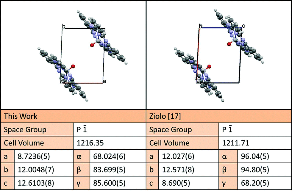 | ||
| Fig. 3 A comparison of the previously published VOPc single crystal structure and the redetermined structure. The upper panels show a view down the longest axis of the unit cell. The parameters are shown below. The different choice of axes is explained in the text. Lengths and volumes are in angstroms and angles are in degrees. | ||
Discussion
In the first instance, we assume that the crystal structure of VOPc is relatively unchanged by the templating process, and that the reflections observed in the diffraction experiments on the films correspond directly to those in the single-crystal structure. The Bragg–Brentano geometry used in these XRD measurements is sensitive only to diffraction occurring from planes near-parallel to the surface. Since the (1) crystal plane is almost normal to the molecular plane, the fact that the (1) reflection is prominent in both films grown on CuI means that the VOPc molecules adopt a ‘standing-up’ orientation with respect to the underlying CuI (111) surface.10,28 This is in stark contrast to the previously reported behaviour of planar MPc molecules on CuI which lie with their molecular planes parallel to the substrate. The samples grown at elevated substrate temperature on CuI surfaces show diffraction from a Miller plane previously unreported in thin films, the (01). The (1) and (21) planes have very similar molecular tilt angles relative to the surface and both imply the molecules are perpendicular to the CuI (111)/SiO2 surface. The additional peak corresponding to the (01) plane means an additional orientation with the molecular plane tilted further towards the surface at an angle of approximately 44°.
This suggests the presence of three distinct orientations in VOPc films prepared at elevated substrate temperatures on CuI. To confirm these assumptions the crystallographic tool of stereographic projections was applied. The stereographic projection showing the three observed planes in VOPc on CuI (Fig. 4) shows that the planes are not close enough to each other in real space to be concurrently observed using the experimental diffraction geometry. Therefore the presence of the planes is due to the preferential orientation of the VOPc molecules into three distinct orientations and is not simply detection of nearly-parallel planes.
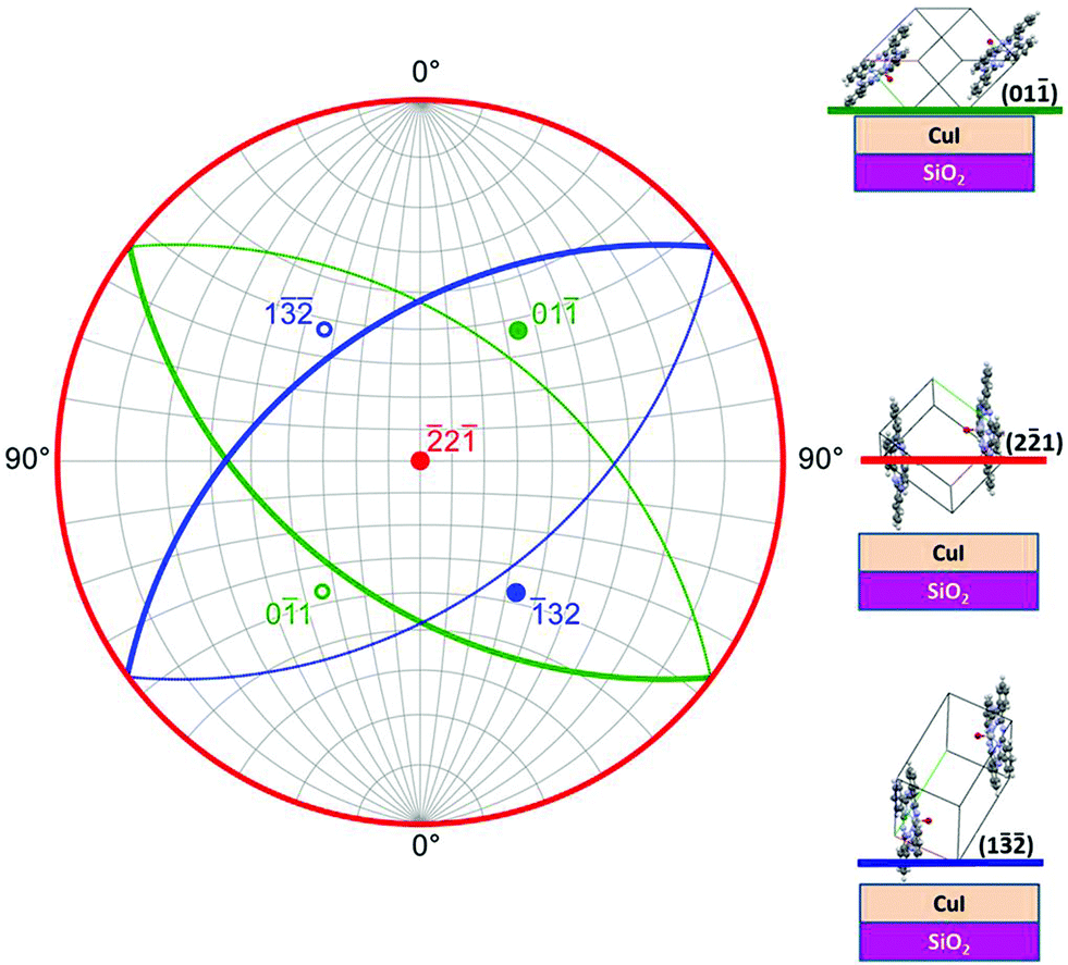 | ||
| Fig. 4 Stereographic projection of the crystallographic planes present in VOPc/CuI bilayers, in direct space. Filled poles and thick traces represent those in the upper hemisphere; hollow poles and thin lines represent those in the lower. Alongside the projection are schematics of the relative molecular orientations seen in these bilayers. The same unit cell is shown in all cases and the planes, of which there are peaks observed in XRD, are indicated with coloured lines and labelled. | ||
In previously reported films of VOPc/SiO2 grown at elevated substrate temperatures {001}-type reflections have been reported.19 In addition to this the (21) plane is seen in XRD patterns of these samples. Of the three distinct diffraction planes present in XRD patterns of elevated substrate temperature VOPc/CuI only one plane (01) is previously unseen in reported films of VOPc. The (1) plane, although previously unreported, is seen in ambient substrate temperature growth of VOPc on CuI. These peaks all have small structure factors (see Fig. S4†) so their presence is indicative of a high degree of orientation within the films.
The behaviour of VOPc has previously been investigated on several (111) surfaces. On Au and Ag (111) surfaces the molecule was found to adopt an orientation where the molecular plane lies flat on the surface and the VO moiety is pointing up, away from the surface.29,30 Similar behaviour has been observed on Si (111) where the molecular plane of VOPc is also parallel to the (111) plane although the VO moiety faces down towards the surface.29 The orientation of VOPc on CuI (111) is therefore very different to that previously seen on other (111) surfaces. The closely related molecule titanyl phthalocyanine (TiOPc) has, however, been shown to adopt a non-parallel orientation on Ag (111).31 TiOPc is similar to VOPc in the presence of a dipole moment out of the plane of the Pc ligand. On Ag (111) it has been suggested that TiOPc deviates from a parallel orientation as it is energetically preferable and minimizes the dipole–dipole repulsion between the molecules. This may also provide an energetic driving force for the unusual behaviour of VOPc on CuI (111).
Previous templating studies of MPcs32 have suggested that the templating effect may be caused by a change in the crystal structure of the MPc film, however no experimental proof has been published. In this case the measured diffraction peaks of VOPc, in templated and untemplated films, could be indexed using the redetermined crystal structure. To assess changes in crystal structure additional thick films of VOPc (around 500–1000 μm), with and without CuI, were grown on Kapton in the same high vacuum sublimation system used for VOPc purification. The resulting films were liberated from the Kapton and XRD experiments were carried out on the resulting powders (Fig. S4†). All of the diffraction peaks present in both powders can be assigned using the redetermined crystal structure, and the diffraction patterns are almost identical. Small changes in intensity can be explained by crystal size variations between the Kapton and CuI/Kapton powders, and differing preferred orientation. Fig. S4† also includes Rietveld fits to the two powder patterns, wherein our redetermined crystal structure is used as a model without structural refinement. Only the lattice parameters, height-offset, scale factor, profile function, background function, and preferred orientation (implemented as 4th order spherical harmonics) were allowed to refine. In other words, neither powder pattern collected in this way is inconsistent with the single-crystal structure we have determined. This leads to the conclusion that although the molecular orientation with respect to the substrate has altered, the crystal structure is still defined by the same unit cell. The insertion of a CuI templating layer, whether grown at ambient or elevated substrate temperature, results in a change in the overall out-of-plane orientation of the VOPc film as shown by XRD measurements.
Acknowledgements
AJR and SH acknowledge support from the Engineering and Physical Sciences Research Council (EPSRC), UK (Grant no. EP/G037515/1). MPR thanks the EPSRC for the award of Grant no. EP/J500161/1. LAR, PS and TSJ acknowledge support from the EPSRC, UK (Grant no. EP/H021388/1). DSK thanks the Science City Research Alliance and the HEFCE Strategic Development Fund for financial support. The PANalytical MPD diffractometer used in this research was obtained through the Science City Energy Futures Project: Hydrogen Energy, with support from Advantage West Midlands (AWM). The Oxford Diffraction Gemini CCD and the Panalytical MRD diffractometers used in this research were obtained through the Science City Advanced Materials Project: Creating and Characterizing Next Generation Advanced Materials, with support from Advantage West Midlands (AWM) and part funded by the European Regional Development Fund (ERDF).References
- S. Heutz, R. Cloots and T. S. Jones, Appl. Phys. Lett., 2000, 77, 3938 CrossRef CAS PubMed.
- S. M. Bayliss, S. Heutz, G. Rumbles and T. S. Jones, Phys. Chem. Chem. Phys., 1999, 1, 3673 RSC.
- W. Wu, L. A. Rochford, S. Felton, Z. Wu, J. L. Yang, S. Heutz, G. Aeppli, T. S. Jones, N. M. Harrison and A. J. Fisher, J. Appl. Phys., 2013, 113, 013914 CrossRef PubMed.
- P. Sullivan, T. S. Jones, A. J. Ferguson and S. Heutz, Appl. Phys. Lett., 2007, 91, 233114 CrossRef PubMed.
- L. Wang, G. Liu, H. Wang, D. Song, B. Yu and D. Yan, Appl. Phys. Lett., 2007, 91, 063511 CrossRef PubMed.
- G. de la Torre, C. G. Claessens and T. Torres, Chem. Commun., 2007, 2000 RSC.
- A. Hoshino, Y. Takenaka and H. Miyaji, Acta Crystallogr., Sect. B: Struct. Sci., 2003, 59, 393 Search PubMed.
- K. Xiao, Y. Liu, G. Yu and D. Zhu, Appl. Phys. A: Mater. Sci. Process., 2003, 77, 367 CrossRef CAS PubMed.
- R. W. I. de Boer, M. E. Gershenson, A. F. Morpurgo and V. Podzorov, Phys. Status Solidi, 2004, 201, 1302 CrossRef CAS.
- B. P. Rand, D. Cheyns, K. Vasseur, N. C. Giebink, S. Mothy, Y. Yi, V. Coropceanu, D. Beljonne, J. Cornil, J.-L. Brédas and J. Genoe, Adv. Funct. Mater., 2012, 22, 2987 CrossRef CAS.
- C. H. Cheng, J. Wang, G. T. Du, S. H. Shi, Z. J. Du, Z. Q. Fan, J. M. Bian and M. S. Wang, Appl. Phys. Lett., 2010, 97, 083305 CrossRef PubMed.
- T.-M. Kim, H. J. Kim, H.-S. Shim, M.-S. Choi, J. W. Kim and J.-J. Kim, J. Mater. Chem. A, 2014, 2, 8730 CAS.
- D. J. Gundlach, Y. Y. Lin, T. N. Jackson, S. F. Nelson and D. G. Schlom, IEEE Electron Device Lett., 1997, 18, 87 CrossRef CAS.
- S. Pfuetzner, J. Meiss, A. Petrich, M. Riede and K. Leo, Appl. Phys. Lett., 2009, 94, 253303 CrossRef PubMed.
- S. M. Schultes, P. Sullivan, S. Heutz, B. M. Sanderson and T. S. Jones, Mater. Sci. Eng., C, 2005, 25, 858 CrossRef PubMed.
- L. A. Rochford, D. S. Keeble, O. J. Holmes, G. J. Clarkson and T. S. Jones, Mater. Sci. Eng., C, 2014, 2, 6056 CAS.
- Y. Zhang, T. Learmonth, S. Wang, A. Y. Matsuura, J. Downes, L. Plucinski, S. Bernardis, C. O'Donnell and K. E. Smith, J. Mater. Chem., 2007, 17, 1276 RSC.
- J. Gantz, D. Placencia, A. Giordano, S. R. Marder and N. R. Armstrong, J. Phys. Chem. C, 2013, 117, 1205 CAS.
- L. Li, Q. Tang, H. Li and W. Hu, J. Phys. Chem. B, 2008, 112, 10405 CrossRef CAS PubMed.
- W. Wang, D. Placencia and N. R. Armstrong, Org. Electron., 2011, 12, 383 CrossRef CAS PubMed.
- F. Pan, H. Tian, X. Qian, L. Huang, Y. Geng and D. Yan, Org. Electron., 2011, 12, 1358 CrossRef CAS PubMed.
- D. A. Duncan, W. Unterberger, K. A. Hogan, T. J. Lerotholi, C. L. A. Lamont and D. P. Woodruff, Surf. Sci., 2010, 604, 47 CrossRef CAS PubMed.
- A. R. McGhie, A. F. Garito and A. J. Heeger, J. Cryst. Growth, 1974, 22, 295 CrossRef CAS.
- O. V. Dolomanov, L. J. Bourhis, R. J. Gildea, J. a. K. Howard and H. Puschmann, J. Appl. Crystallogr., 2009, 42, 339 CrossRef CAS.
- G. M. Sheldrick, Acta Crystallogr., Sect. A: Found. Crystallogr., 2008, 112 CrossRef CAS PubMed.
- A. Coelho, Topas Academic V4, 2008, http://www.topas-academic.net Search PubMed.
- R. F. Ziolo, C. H. Griffiths and J. M. Troup, J. Chem. Soc., Dalton Trans., 1980, 33, 2300 RSC.
- K. Vasseur, K. Broch, A. L. Ayzner, B. P. Rand, D. Cheyns, C. Frank, F. Schreiber, M. F. Toney, L. Froyen and P. Heremans, ACS Appl. Mater. Interfaces, 2013, 5, 8505 CAS.
- L. A. Rochford, I. Hancox and T. S. Jones, Surf. Sci., 2014, 628, 62 CrossRef CAS PubMed.
- K. Eguchi, Y. Takagi, T. Nakagawa and T. Yokoyama, J. Phys. Chem. C, 2013, 117, 22843 CAS.
- Y. Wei, S. W. Robey and J. E. Reutt-Robey, J. Phys. Chem. C, 2008, 112, 18537 CAS.
- S. W. Cho, A. DeMasi, A. R. H. Preston, K. E. Smith, L. F. J. Piper, K. V. Chauhan and T. S. Jones, Appl. Phys. Lett., 2012, 100, 263302 CrossRef PubMed.
Footnotes |
| † Electronic supplementary information (ESI) available: AFM and XRD of CuI films grown at 25 °C. Pole figures of CuI films grown at 155 °C. XRD and AFM of VOPc films grown at 25 °C and 155 °C on SiO2. Powder diffraction data of VOPc grown on CuI and Kapton. CCDC 1017243. For ESI and crystallographic data in CIF or other electronic format see DOI: 10.1039/c4tc02116a |
| ‡ The manuscript was written through contributions of all authors. All authors have given approval to the final version of the manuscript. |
| This journal is © The Royal Society of Chemistry 2015 |