
 Open Access Article
 This Open Access Article is licensed under a
 Creative Commons Attribution 3.0 Unported Licence
Rapid perovskite formation by CH3NH2 gas-induced intercalation and reaction of PbI2†
Sonia R.
Raga‡
,
Luis K.
Ono‡
and
Yabing
Qi
*
Energy Materials and Surface Sciences Unit (EMSS), Okinawa Institute of Science and Technology Graduate University (OIST), 1919-1 Tancha, Onna-son, Kunigami-gun, Okinawa 904-0495, Japan. E-mail: Yabing.Qi@OIST.jp
First published on 21st December 2015
Abstract
Solution processable perovskite solar cells traditionally use CH3NH3I solid powder as one of the two precursors that requires solvation into a solution and a spin-coating step; the resulting films need post-annealing (∼1 h) for complete conversion to CH3NH3PbI3. Here we describe for the first time the formation of stoichiometric perovskite in ambient air by exposing PbI2 films to a simple CH3NH2 gas precursor (as opposed to CH3NH3I solid powders). The reaction completes within a few seconds forming complete-coverage perovskite films with a roughness of 2 nm. The non-stoichiometric reaction produces Pb oxides as by-products, which are reconverted by further HI gas exposure. With combined measurements of the thin film crystal structure, chemical state, and absorption properties, we elucidate the chemical reaction mechanisms underlying these gas-induced processes. Fabricated solar cell devices show an efficiency of 15.3%, which remains almost the same after 133 days. Such a gas-induced reaction also enabled the successful preparation of high quality perovskite films with a size of 100 cm2.
Introduction
Methylammonium lead halide CH3NH3PbX3 (X = I and Br) perovskite solar cells are currently at the forefront of solar cell research because of their numerous desirable properties and are a promising candidate for next-generation photovoltaic technology.1–4 With only a few years of research, perovskite solar cell efficiencies have rapidly increased to a level that is on par with even the best crystalline silicone solar cells.5,6 At present, solution processing is the most widely employed technique for the fabrication of perovskite layers.7,8 In solution processing, two solid powder precursors, methylammonium halides (CH3NH3X, X = I and Br) and lead halides (PbX2, X = I, Br, and Cl), are dissolved into solutions and spin-coated on substrates. A subsequent post-annealing step (typically ∼1 h) is required for the complete conversion to CH3NH3PbX3. Solution processing techniques, especially the related spin-coating technique, are difficult to scale up, which makes them unsuitable for mass-production of large-area solar cells. The industrial-scale manufacturing of perovskite solar cells urgently calls for a new method that is suitable to coat high-quality perovskite films over a large area (e.g. 1 cm2 or larger).4In this work, we report a novel method that is capable of forming uniform perovskite films in ambient air over a large area. It is achieved by exposing PbI2 films to a CH3NH2 gas precursor (referred to as the MA step hereafter). Such a gas-induced reaction exhibits multiple advantages over the solution processing using the conventional CH3NH3I solid powder precursor. First of all, the MA step typically completes within a few seconds due to the two-dimensional (2D) characteristics (layered structure) of PbI2 films.9–13 In general, 2D materials possess the characteristics of strong in-plane chemical bonds and weak van der Waals inter-plane interactions. The observation that CH3NH3PbI3 perovskites are formed within merely a few seconds is a direct manifestation of the benefit of the gas intercalation process owing to the high permeability of CH3NH2 gas and the 2D layered structure of PbI2 films that enables CH3NH2 to quickly (1) diffuse through grain boundaries of polycrystalline PbI2 crystals and (2) subsequently to enter inside every PbI2 crystallite. Secondly, because of the gas-induced reaction nature (as opposed to CH3NH3I solid powder), it allowed the successful preparation of high-quality perovskite films with a size of 100 cm2. Thirdly, using different starting lead/tin halide films reacting with CH3NH2 as well as additional exposure to HI or HBr, our method enabled the formation of a wide range of perovskite materials (CH3NH3PbCl3, CH3NH3PbBr3, CH3NH3PbI3, CH3NH3SnBrxI3−x, CH3NH3PbBrxI3−x, and CH3NH3PbBrxCl3−x). These materials exhibited tunable optical properties that are attractive for window photovoltaic as well as other optoelectronic applications such as light-emitting diodes and lasers.14–17 Fourthly, in comparison with solution processing, our method requires neither the synthesis of CH3NH3I nor post-annealing treatment resulting in a much simpler and faster process for perovskite fabrication (within 15 minutes), which helps reduce cost. Last but not least, using X-ray diffraction (XRD), X-ray photoelectron spectroscopy (XPS) and UV-visible spectroscopy (UV-Vis), we propose the chemical reaction mechanisms underlying these gas-induced reactions that are in good agreement with experimental observations.
Experimental
PbI2 layer fabrication
PbI2 was dissolved in dimethylformamide (DMF, 460 mg mL−1) and kept stirring at 70 °C until it completely dissolved. The PbI2 solution was spin coated on the substrates (glass or FTO/compact layer TiO2/mesoporous TiO2), previously heated at 70 °C, at 4000 rpm for 30 s and then dried on a hot plate at 70 °C for 5 minutes in a N2 glovebox. The substrates were taken out to air for perovskite formation by subsequent MA and HI steps as well as Processes P1 and P2 described below.MA step
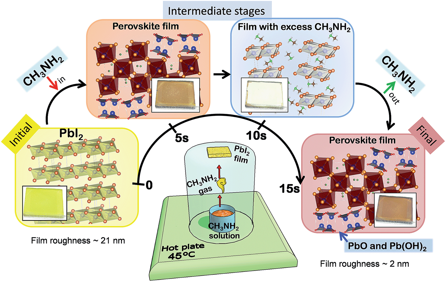 | ||
| Fig. 1 Methylamine gas induced perovskite formation. Illustration of the setup used for processing perovskite at room temperature from simple precursors of CH3NH2 gas and the PbI2 film is depicted in the lower middle part of the figure: a PbI2 film pre-deposited on mp-TiO2/cl-TiO2/FTO is exposed to CH3NH2 gas from a heated solution. The different stages of the reaction are schematized from left to right with an arrow corresponding to the time scale of the process. Upon CH3NH2 gas exposure, the characteristic yellow colored PbI2 film turns dark after 5 s. At this point, CH3NH3PbI3 perovskite, PbO and Pb(OH)2 are formed. After subsequent 10 s exposure, the film becomes transparent and associated with the incorporation of excess CH3NH2 into the lattice. Once the sample is removed from the CH3NH2 exposure, the film becomes dark red/brown in color within 5 s with a mirror-like surface. | ||
HI step
Process P1
Process P2
TiO2 substrate fabrication
Glass coated with fluorine-doped SnO2 (FTO, 15 Ohm sq.−1) was first etched using Zn and HCl and cleaned by sequential sonication in a soapy bath, Milli-Q water and isopropanol. The FTO was covered with a 70 nm compact layer of TiO2 by a spray pyrolysis method using a precursor solution composed of acetylacetone, Ti(IV) isopropoxide and anhydrous ethanol (3![[thin space (1/6-em)]](https://www.rsc.org/images/entities/char_2009.gif) :3:2 wt). A 150 nm-thick TiO2 mesostructured (mp-TiO2) layer was deposited by spin-coating a diluted TiO2 paste (Dyesol, 90-T) and then annealed at 450 °C for 30 min.
:3:2 wt). A 150 nm-thick TiO2 mesostructured (mp-TiO2) layer was deposited by spin-coating a diluted TiO2 paste (Dyesol, 90-T) and then annealed at 450 °C for 30 min.
Solar cell fabrication
The perovskite was deposited on the mp-TiO2 following MA and HI steps and Processes P1 and P2. The hole transport layer was deposited by spin coating at 2000 rpm a chlorobenzene solution containing 59 mM 2,2′,7,7′-tetrakis(N,N′-di-p-methoxyphenylamine)-9,9′-spirobifluorene (spiro-OMeTAD), 172 mM tert-butylpyridine and 32 mM of Li-bis(trifluoromethanesulfonyl)-imide salt pre-dissolved in acetonitrile. The top contact was fabricated by thermal evaporation of gold, with a final thickness of 80 nm. The devices were not sealed.Characterization
The film crystallinity was analyzed by XRD (D8 Bruker) with a diffraction angle resolution of 0.01°. UV-Vis absorbance measurements were taken with a spectrophotometer Evolution 600, Thermo Scientific at intervals of 0.2 nm. The measured relative humidity and temperature of the laboratory were 50% and 25 °C, respectively. The surface morphology was measured by using an atomic force microscope (AFM) from Asylum instruments using tapping mode cantilevers with a nominal spring constant of 48 N m−1. For high resolution XPS (HR-XPS) measurements, we used a monochromated Al-Kα (hν = 1486.6 eV) excitation source. The system comprises a delay-line detector with a 180° hemispherical, 165 mm mean radius analyzer, AXIS Ultra DLD (Kratos Surface Analysis). Binding energy scales for XPS were calibrated by measuring the Fermi edge (EF = 0 eV) and Au-4f7/2 (84.0 eV) on a clean Au surface. Energy resolution was less than 0.5 eV for HR-XPS. X-ray induced sample damage was monitored by taking five consecutive spectra and comparing them. Acquisition time for each scan varied from 10 to 20 s, depending on the core level regions. The five scans were averaged to a single spectrum if no changes were observed among them. Analysis of XPS data was performed in CasaXPS 2.3.16 software. Shirley-type background was subtracted to account for inelastic scattering processes. The atomic concentrations of different chemical elements were extracted from XPS intensity ratios after appropriate normalization using atomic sensitivity factors.Current–voltage (j–V) characteristics of solar cells were measured under 1-sun illumination (AM 1.5G, 100 mW cm−2) in air using a xenon-lamp (USHIO, UXL-150SO) based solar simulator (Newport Oriel Sol 1A) and a Keithley 2420 source meter. The solar simulator illumination intensity was calibrated using a monocrystalline silicon cell (Oriel Instruments Model Number 90026564, 2 × 2 cm2) calibrated by NREL. Influences of voltage scan conditions and pre-illumination were tested and described in Fig. S9.† Unless stated, the voltage scan was performed from 1.2 V to 0 V (named reverse scan) at 0.1 V s−1, with a dwell time of 5 ms and pre-illumination of 5 s. All measurements were performed in air at room temperature and cells without encapsulation. The effective active areas of the devices ranged between 0.05 and 0.18 cm2, and all measurements were performed without a mask. The external quantum efficiency (EQE) was measured using an Oriel IQE-200 measurement system from 850 to 300 nm in a 10 nm step.
Results and discussion
Detailed procedures are provided in the Experimental section. Briefly, a PbI2 film spin-coated on a FTO/compact layer TiO2/mesoporous TiO2 substrate was exposed to CH3NH2 gas. The CH3NH2 gas-exposed PbI2 film is named Sample #1 and this process is named MA step (Fig. 1 and Table 1) hereafter. A simple setup, shown in Fig. 1, was used for confining the CH3NH2 gas inside a beaker with the substrate affixed at the bottom inside a beaker and facing upside down. The CH3NH2 gas was generated by heating the CH3NH2 solution at 45 °C using a hot plate. The MA step completes within a few seconds generating a dark-red/brown color with semi-transparent hue, similar to that of CH3NH3PbI3 perovskite films synthesized by spin coating using CH3NH3I and PbI2 precursors.18 Using the MA step, we were able to form a high-quality mirror-like semi-transparent perovskite film on a large substrate with a size of 100 cm2 (ESI Fig. S1†) in a few seconds, clearly demonstrating the potential of this method for large-area solar cell mass-production. We propose that because of the small size and high vapor pressure (350 kPa, 25 °C) of CH3NH2 gas molecules, they easily permeate into the PbI2 film.| Sample name | Treatment | PCE (%) | j sc (mA cm−2) | V oc (V) | FF |
|---|---|---|---|---|---|
| #1 MA step | MA gas exposure on the PbI2 film | 6.8 ± 0.7 [7.6] | 14.4 ± 1.3 [14.2] | 1.03 ± 0.01 [1.02] | 0.47 ± 0.04 [0.52] |
| #2 HI step | Subsequent HI gas exposure | 6.9 ± 1.2 [8.9] | 12.1 ± 0.7 [12.5] | 1.03 ± 0.03 [1.05] | 0.60 ± 0.09 [0.68] |
| #3 Process P1 | Sequential HI gas + MA gas exposure | 9.4 ± 1.8 [12.7] | 19.1 ± 2.7 [22.8] | 1.01 ± 0.02 [1.01] | 0.53 ± 0.03 [0.56] |
| #4 Process P2 | Simultaneous HI gas + MA gas exposure | 13.5 ± 1.1 [15.3] | 19.0 ± 0.9 [20.6] | 1.04 ± 0.01 [1.05] | 0.69 ± 0.03 [0.71] |
The resulting films of Samples #1 were extremely uniform and smooth with a mirror-like appearance. The smoothness was further confirmed by atomic force microscopy (AFM) measurements (ESI Fig. S2a and b†). The morphology of the initial PbI2 films showed a root mean square (RMS) surface roughness of ∼21 nm, that became ∼10 times smoother after the MA step. The RMS roughness of Samples #1 was determined to be ∼2 nm, which explains the mirror-like pinhole-free appearance. An amorphous, liquid phase has been observed previously upon perovskite crystal exposure to MA gas, which improves the perovskite film coverage and surface roughness.19 Despite the smoothness of the films, the crystalline features (grain sizes) in Samples #1 were extremely small and in the range of 40–70 nm. Solar cell devices employing the films synthesized by only the MA step (i.e. no further treatments) as absorbers with subsequent stacked layers of spiro-OMeTAD and Au as a hole transport layer (HTL) and electrode, respectively, generated power conversion efficiencies (PCEs) as high as 7.6% with a short-circuit current density (jsc) of 14.2 mA cm−2, an open-circuit voltage (Voc) of 1.02 V, and a fill factor (FF) of 0.52 (Fig. 2f and Table 1). As will be described in detail later, the major composition of the films after the MA step is indeed stoichiometric CH3NH3PbI3 perovskite. However, additional lead oxide and Pb(OH)2 phases were also observed to form and distributed in the films as a result of the MA step. The lead oxide and Pb(OH)2 phases were formed as a byproduct based on the proposed reaction (1a) and the alternative reaction pathways (1b and 1c),20 which are in good agreement with our experimental results of the thin film crystal structure, chemical state, and absorption properties.
| 3PbI2 + 2CH3NH2 + H2O → 2CH3NH3PbI3 + PbO | (1a) |
| CH3NH2 + H2O → CH3NH3OH | (1b) |
| 3PbI2 + 2CH3NH3OH → 2CH3NH3PbI3 + Pb(OH)2 | (1c) |
| PbO + 2HI → PbI2 + H2O | (1d) |
| Pb(OH)2 + 2HI → PbI2 + 2H2O | (1e) |
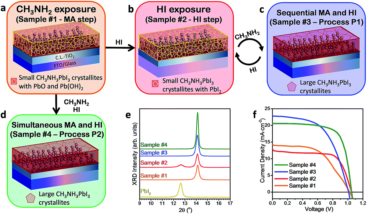 | ||
| Fig. 2 Illustration of post-treatments of HI exposure and Processes P1 and P2 and corresponding solar cell performances. Overview of all the post-treatment processes is described in the text. (a) Exposure of the PbI2 film to CH3NH2 gas at room temperature (25 °C) generates perovskite and PbO/Pb(OH)2 with characteristic grain sizes in the range of 40 nm and a RMS surface roughness of ∼2 nm (Sample #1 – the MA step). (b) Sample #1 exposed to HI gas at 70 °C re-converts the PbO/Pb(OH)2 to PbI2 (Sample #2 – the HI step). (c) Sample #1 exposed sequentially to MA and HI gradually converts the PbO/Pb(OH)2 first to PbI2 and eventually to perovskite crystals of ∼400 nm in size and ∼14 nm surface roughness (Sample #3 – Process P1). (d) Sample #1 exposed simultaneously to MA and HI at 70 °C forms a smooth perovskite film with a grain size of ∼200 nm and roughness of ∼6 nm. (e) XRD and (f) j–V curves of solar cells fabricated based on films (a–d). The measurements were conducted under AM 1.5 (100 mW cm−2) illumination conditions (see the Experimental section for more details). | ||
The fact that the MA step can proceed even at room temperature (ESI Fig. S3†) clearly suggests its spontaneity, i.e. the formation of stoichiometric perovskite and PbO/Pb(OH)2 is thermodynamically more favorable as opposed to both (1) the reactants PbI2, MA and H2O and (2) the formation of non-stoichiometric perovskite containing a large number of iodine vacancies (i.e. PbI2 + MA → MAPbI2). We further introduced additional post-treatments (Fig. 2a–d) of sequential HI gas exposure (the HI step generating Samples #2), sequential HI gas and MA gas exposure (Process P1 generating Samples #3), and simultaneous HI gas and MA gas exposure (Process P2 generating Samples #4), which have shown to be efficient methodologies to convert the additional lead oxide and Pb(OH)2 phases to PbI2 and perovskite (Fig. 2a–d). If the number of cycles is not specified, Process P1 refers to a single sequential cycle of HI gas and MA gas exposure. Solar cells prepared by the HI step showed the best efficiency of 8.9% with a Voc of 1.05 V, a jsc of 12.5 mA cm−2, and a FF of 0.68 (Fig. 2f and Table 1). In particular, the large increase of the FF compared to Samples #1 confirms better charge transport properties of PbI2 than lead oxide and Pb(OH)2.21 The slight decrease in jsc (14.4 mA cm−2 → 12.1 mA cm−2) may be correlated with some perovskites being reconverted to PbI2 in the HI step lowering the photocurrent generation. In contrast to the slight efficiency improvement by the HI step, both Processes P1 and P2 led to substantial improvement in solar cell performance, with the best cell achieving an efficiency of 15.3% with a Voc of 1.05 V, a jsc of 20.6 mA cm−2, and a FF of 0.71 (Fig. 2f and Table 1). The device retained an efficiency of 14.6% after >3000 h stored in a glove box (ESI Fig. S8†), with an integrated jsc of 17.0 mA cm−2 extracted from external quantum efficiency (EQE) and a steady current at a peak point of 16.5 mA cm−2 (ESI Fig. S4†). These processes (Processes P1 and P2) are fast, simple (without the need to synthesize MAI), and low-cost and can be easily scaled up to mass-production of large-area cells.
The physico-chemical properties of the synthesized films from the MA and HI steps as well as Processes P1 and P2 (corresponding to Samples #1–#4, respectively) were investigated in detail by XRD (Fig. 2e), UV-Vis (ESI Fig. S2e†), XPS (ESI Fig. S2f†), and AFM (ESI Fig. S2a–d†). XRD measurements (Fig. 2e) performed on the PbI2 film before and after the MA step confirmed the conversion to the tetragonal perovskite crystal with no residual PbI2.22,23 The XRD peaks at 14.1° and 28.5° peaks matched well with the reported (110) and (220) crystal peaks, respectively, of stoichiometric CH3NH3PbI3 perovskite films prepared by the standard method, i.e. the reaction between PbI2 and CH3NH3I.23 The UV-Vis absorption data (ESI Fig. S2e†) showed a sharp absorption edge at 775 nm corresponding to a bandgap of 1.6 eV in good agreement with the previous reports on CH3NH3PbI3 perovskite.24 We also studied the effect of post-annealing on the crystallinity of Samples #1 formed at 24 °C, the results of which can be found in the ESI Fig. S3†. Our analysis indicates that the perovskite crystals formed in Samples #1 are stoichiometric CH3NH3PbI3 and did not have an appreciable number of iodine vacancies. This result seems counter-intuitive that the MA step involving only PbI2 and CH3NH2 can form stoichiometric CH3NH3PbI3 perovskite. On the other hand, the reaction underlying the MA step can be hinted at by our observation that perovskite can only be formed by performing the MA step in ambient air (i.e. in the presence of H2O) as described in reaction (1a). To highlight the importance of H2O in the reaction, a control experiment of the MA step was performed in a dry environment such as in a N2 glovebox with H2O levels below 0.1 ppm (ESI Fig. S5†). No perovskite formation was observed during this control experiment, which is in good agreement with the previously reported study performed with a vacuum system.11
XPS analysis of the resulting films from the MA step confirmed the formation of lead oxide and Pb(OH)2 phases on Samples #1, which is consistent with the two proposed reaction pathways (1a) and (1b) + (1c) (ESI Fig. S6a and c† – O 1s core-level regions). In fact, only Samples #1 showed the presence of two oxidation states in the XPS O 1s core-level region. The low binding energy (BE) peak at 529.7 eV (O1) was assigned to PbO, while the high BE peak at 531.5 eV (O2) was assigned to Pb(OH)2 (1c) formation with possible contributions from PbxOy compounds as well.25–27 More than twenty lead oxide compounds were reported to exist without a defined stoichiometry. This is consistent with the fact that the full width at half maximum (FWHM) value of peak O2 (1.9 eV) is significantly larger than that of peak O1 (FWHM = 0.6 eV). In those compounds, the crystallographic valence of the oxygen in the lattice adopts a wide range of values (O−1.89 to O−2.25).27 Due to such variations, it is challenging to determine the crystal and electronic structures of these lead oxide compounds. For the sake of simplicity, in the discussion hereafter, we will use PbO as an example of the product in (1a) to illustrate, even though other PbxOy products are also very likely formed in Samples #1. XPS atomic ratios normalized with respect to Pb (ESI Fig. S2f†) were calculated based on the peak areas and with appropriate normalization taking into account atomic sensitivity factors. On the basis of the [O]/[Pb] and [I]/[Pb] values, the total amount of lead oxide and Pb(OH)2 was calculated to be ∼24 mol% that coexists with perovskite in Samples #1. This is in good agreement with the proposed reactions (1a) and (1c), in which a nominal ∼33 mol% of lead oxide and Pb(OH)2 would be expected.
The corresponding XRD results from Samples #2 (Fig. 2e) reveal the formation of PbI2 crystals from the transformation of lead oxide and Pb(OH)2 phases following chemical reactions (1d) and (1e) or by the iodination process due to the co-existence of I2 gas in the HI fume.28 The peaks in the XPS O 1s core level region in Samples #1 became much smaller after the HI step (2–10 min) (ESI Fig. S2f, S6b and S7†), which corroborates the proposed reactions (1d) and (1e). Extra care was taken to minimize the exposure of freshly prepared samples to ambient air when transferring to the XPS measurement system. We excluded the possibility that oxygen signals in Samples #1 can come from contamination or water adsorption because they are present only in Samples #1, but not in Samples #2. The iodine incorporation can also be reflected by an overall increase of the optical absorbance of the films below ∼775 nm, which was observed to saturate after performing the HI step for ∼4 min (ESI Fig. S2f and S7†). Finally, much purer CH3NH3PbI3 perovskite was formed after the subsequent Processes P1 and P2, which is confirmed by XRD with no residual PbI2 (Fig. 2e). XPS confirmed the perovskite film formation. The saturated [I]/[Pb] ratio was close to 2.5 (ESI Fig. S2f†). The deviation from the expected [I]/[Pb] ratio of 3 could be attributed to several factors such as (i) XPS is surface sensitive (∼5 nm) and the surface chemical composition can be different from the bulk chemical composition. Possibly for a similar reason, we observed the [N]/[Pb] ratio also deviating from 1; (ii) the Pb 4f region shows convoluted Pb2+ states from perovskite and lead oxide and Pb(OH)2. Thus, the [I]/[Pbtotal] shows a smaller ratio. Indeed we noticed that some amount of lead oxide and Pb(OH)2 was formed after each cycle in Samples #3 (ESI Fig. S6c†). However, the amount is reduced rapidly after each cycle of Process P1. On the basis of chemical reactions (1a) and (1c), after each cycle of Process P1 the lead oxide phase is expected to reduce by ∼67%. For instance, 3 cycles of Process P1 are sufficient to bring the molar concentration of lead oxide phase down to 3.6 mol%. This trend of reducing PbO is well aligned with the increased PCE with the number of Process P1 cycles performed (ESI Fig. S8 and Table S1†). In addition, we performed AFM measurements to study the crystal grain size and observed that the sequential and complete cycles of Process P1 and simultaneous MA and HI exposure of Process P2 in air produced a gradual increase of the CH3NH3PbI3 crystal grains up to ∼200–400 nm (ESI Fig. S2c and d†).
In addition, our method is found to be universal forming a wide variety of perovskite materials (CH3NH3PbCl3, CH3NH3PbBr3, CH3NH3PbI3, CH3NH3SnBr3 CH3NH3PbBrxI3−x, and CH3NH3PbBrxCl3−x). For example, we performed the MA step to convert the initial PbBr2 and PbCl2 films into CH3NH3PbBr3 and CH3NH3PbCl3 perovskites, respectively (Fig. 3a). It was found that the time scale for CH3NH2 intercalation into the Pb halide was much slower for the PbCl2 (∼180 s) than PbBr2 (∼60 s) and PbI2 (∼15 s) suggesting that the formation of iodine-based perovskite is more favorable than the Br and Cl counterparts. When the MA step-treated PbCl2 (CH3NH3PbCl3) film was exposed to HI, only XRD peaks corresponding to CH3NH3PbI3 could be observed.18 Furthermore, we were able to generate mixed-perovskite halides using our method by re-converting the ∼33% PbO and Pb(OH)2 formed by the MA step by exposing to HI or HBr gas. For example, a PbBr2 film initially exposed to MA gas was subsequently exposed to HI gas in a stepwise manner inducing the gradual formation of CH3NH3PbBr3−xIx perovskite. Fig. 3b shows the gradual band-gap tuning of the CH3NH3PbBr3−xIx perovskite film. Long exposure times caused the optical absorption edge to saturate at 690 nm. We attributed this saturation to the formation of CH3NH3PbBr2I perovskite, where iodine substituted all of the 33% PbO and Pb(OH)2 formed during the MA step. The XRD data (Fig. 3c) for the mixed Br:I perovskite showed a shift in the peak position, indicating that Br- and I-based perovskites are mixed rather than segregated. This suggests that HI gas permeates easily into the bulk of the film generating uniformly mixed Br:I perovskite. In contrast, the CH3NH3PbCl3 film with PbO and Pb(OH)2 exposed briefly to HBr led to the appearance of two XRD peaks at 15° and 15.6°, which were assigned to the two segregated phases of CH3NH3PbBr3 and CH3NH3PbCl3 perovskites, respectively.18 In the case of SnBr2, the conversion was not possible in air because the formation of SnO and CH3NH3Br was more favorable. When we performed the MA step in a N2 glovebox followed by HI gas exposure, the conversion to CH3NH3SnBrxI3−x perovskite was successful, but a certain amount of SnI2 was also generated additionally.
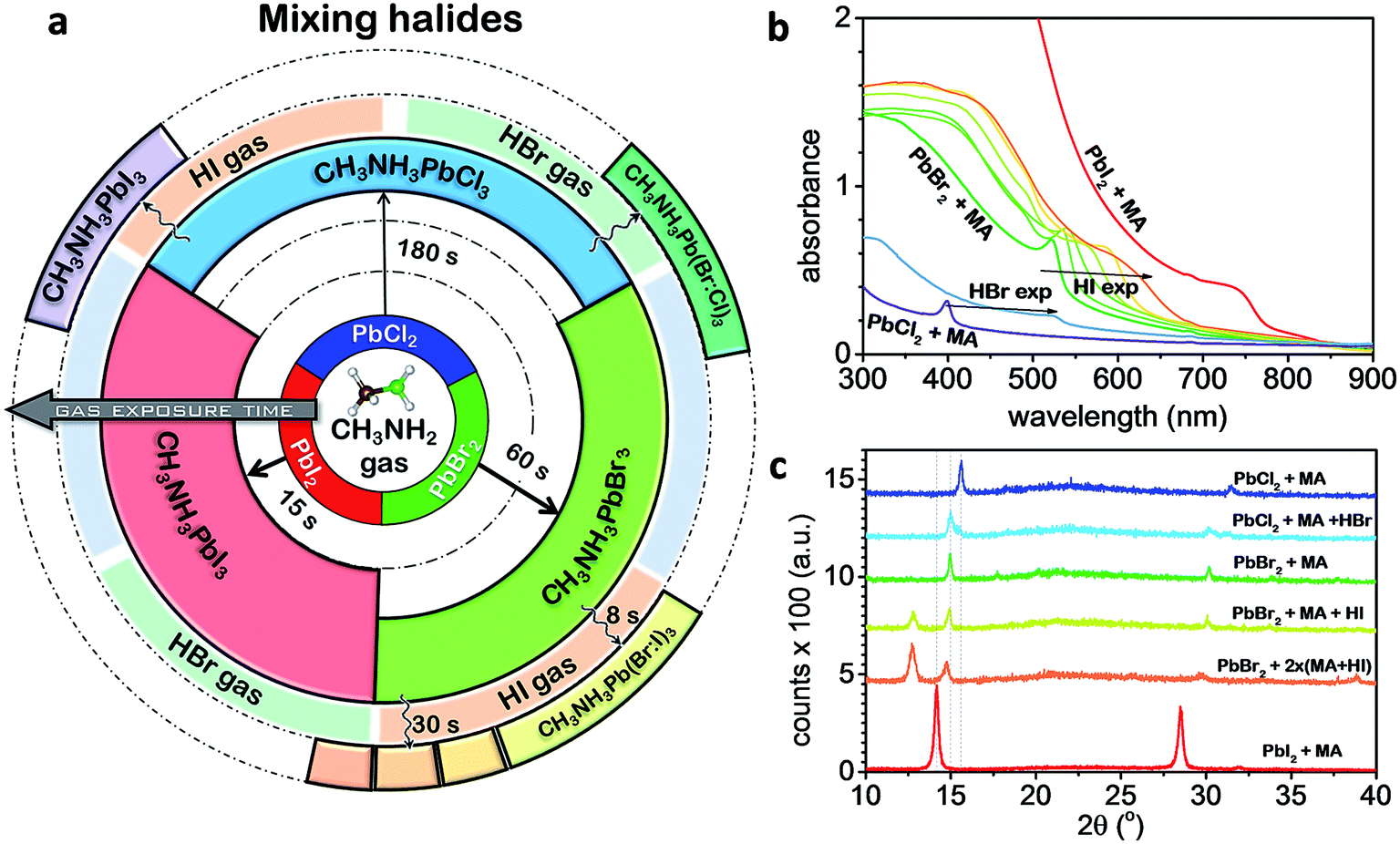 | ||
| Fig. 3 Perovskite conversion from PbX2 (X = I, Br, and Cl) films exposed to CH3NH2 gas and to HI and HBr gases. (a) Scheme representing all the possibilities of lead halide exposures to CH3NH2 and hydrogen halide gases. After the initial conversion of PbX2 to CH3NH3PbX3 + PbO/Pb(OH)2 upon CH3NH2 gas exposure, the perovskite can be finely tuned to mixed-halide perovskite, by converting PbO/Pb(OH)2 to PbI2 or PbBr2 after HI or HBr gas exposures, respectively. The reactions happen at different time-scales depending on the halide: I (15 s) < Br (60 s) < Cl (180 s) with iodine-based perovskite conversion the fastest among all. Addition of chlorine is not favorable to form uniformly mixed-halide perovskite, but only phase-segregated perovskites. (b) Absorbance spectra and (c) XRD of selected films of mixed-halide perovskites. | ||
Conclusions
We showed the role and interplay of three simple precursors, i.e. PbI2, methylamine (CH3NH2, MA) gas, and hydroiodic (HI) gas for the formation of high quality perovskite films. MA gas (instead of the well-known precursor CH3NH3I), in ambient air, reacts directly with PbI2 to form stoichiometric CH3NH3PbI3 perovskite (the MA step). Because of the high permeability of the MA gas and the 2D layered structure of PbI2, the reaction completes within a few seconds. The MA step also leads to the formation of a relatively large amount of lead oxide (33 mol%) as a byproduct. Nevertheless, even with such a large amount of lead oxide, solar cells based on the MA step reached an efficiency of 7.6%. We further introduced post-treatments such as HI gas exposure, sequential and simultaneous HI and MA gas exposures. The post-treatments led to substantially improved performance with a negligible content of PbI2 or Pb-oxides, with the best cell achieving efficiency of 15.3% and outstanding stability after 133 days.Acknowledgements
This work was supported by funding from the Energy Materials and Surface Sciences Unit of the Okinawa Institute of Science and Technology Graduate University and JSPS KAKENHI Grant Number 15K17925.References
- J. H. Heo, S. H. Im, J. H. Noh, T. N. Mandal, C. S. Lim, J. A. Chang, Y. H. Lee, H. J. Kim, A. Sarkar, M. K. Nazeeruddin, M. Gratzel and S. I. Seok, Nat. Photonics, 2013, 7, 487–492 CrossRef.
- O. Malinkiewicz, A. Yella, Y. H. Lee, G. M. Espallargas, M. Graetzel, M. K. Nazeeruddin and H. J. Bolink, Nat. Photonics, 2014, 8, 128–132 CrossRef.
- D. Y. Liu and T. L. Kelly, Nat. Photonics, 2014, 8, 133–138 CrossRef CAS.
- M. A. Green, A. Ho-Baillie and H. J. Snaith, Nat. Photonics, 2014, 8, 506–514 CrossRef CAS.
- W. S. Yang, J. H. Noh, N. J. Jeon, Y. C. Kim, S. Ryu, J. Seo and S. I. Seok, Science, 2015, 348, 1234–1237 CrossRef CAS PubMed.
- H. Zhou, Q. Chen, G. Li, S. Luo, T.-b. Song, H.-S. Duan, Z. Hong, J. You, Y. Liu and Y. Yang, Science, 2014, 345, 542–546 CrossRef CAS PubMed.
- M. M. Lee, J. Teuscher, T. Miyasaka, T. N. Murakami and H. J. Snaith, Science, 2012, 338, 643–647 CrossRef CAS PubMed.
- J. Burschka, N. Pellet, S. J. Moon, R. Humphry-Baker, P. Gao, M. K. Nazeeruddin and M. Gratzel, Nature, 2013, 499, 316–319 CrossRef CAS PubMed.
- M. Ogawa and K. Kuroda, Chem. Rev., 1995, 95, 399–438 CrossRef CAS.
- J. Y. Zhang, T. Song, Z. J. Zhang, K. Ding, F. Huang and B. Q. Sun, J. Mater. Chem. C, 2015, 3, 4402–4406 RSC.
- R. F. Warren and W. Y. Liang, J. Phys.: Condens. Matter, 1993, 5, 6407–6418 CrossRef CAS.
- G. I. Gurina and K. V. Savchenko, J. Solid State Chem., 2004, 177, 909–915 CrossRef CAS.
- Y. Zhao and K. Zhu, Chem. Commun., 2014, 50, 1605–1607 RSC.
- R. F. Service, Science, 2014, 344, 458 CrossRef PubMed.
- Z.-K. Tan, R. S. Moghaddam, M. L. Lai, P. Docampo, R. Higler, F. Deschler, M. Price, A. Sadhanala, L. M. Pazos, D. Credgington, F. Hanusch, T. Bein, H. J. Snaith and R. H. Friend, Nat. Nanotechnol., 2014, 9, 687–692 CrossRef CAS PubMed.
- G. Xing, N. Mathews, S. S. Lim, N. Yantara, X. Liu, D. Sabba, M. Grätzel, S. Mhaisalkar and T. C. Sum, Nat. Mater., 2014, 13, 476–480 CrossRef CAS PubMed.
- L. K. Ono, S. H. Wang, Y. Kato, S. R. Raga and Y. B. Qi, Energy Environ. Sci., 2014, 7, 3989–3993 CAS.
- S. R. Raga, M.-C. Jung, M. V. Lee, M. R. Leyden, Y. Kato and Y. B. Qi, Chem. Mater., 2015, 27, 1597–1603 CrossRef CAS.
- Z. Zhou, Z. Wang, Y. Zhou, S. Pang, D. Wang, H. Xu, Z. Liu, N. P. Padture and G. Cui, Angew. Chem., Int. Ed., 2015, 54, 9705–9709 CrossRef CAS PubMed.
- N. Feltin and M. P. Pileni, Langmuir, 1997, 13, 3927–3933 CrossRef CAS.
- Q. Chen, H. P. Zhou, T. B. Song, S. Luo, Z. R. Hong, H. S. Duan, L. T. Dou, Y. S. Liu and Y. Yang, Nano Lett., 2014, 14, 4158–4163 CrossRef CAS PubMed.
- N. Onoda-Yamamuro, T. Matsuo and H. Suga, J. Phys. Chem. Solids, 1992, 53, 935–939 CrossRef CAS.
- T. Baikie, Y. Fang, J. M. Kadro, M. Schreyer, F. Wei, S. G. Mhaisalkar, M. Graetzel and T. J. White, J. Mater. Chem. A, 2013, 1, 5628–5641 CAS.
- M. Liu, M. B. Johnston and H. J. Snaith, Nature, 2013, 501, 395–398 CrossRef CAS PubMed.
- X-ray Photoelectron Spectroscopy Database, Version 3.4 (Web Version), http://www.srdata.nist.gov/xps/index.htm.
- J. M. Luther, M. Law, Q. Song, C. L. Perkins, M. C. Beard and A. J. Nozik, ACS Nano, 2008, 2, 271–280 CrossRef CAS PubMed.
- R. A. Evarestov and V. A. Veryazov, Phys. Status Solidi B, 1991, 165, 401–410 CrossRef CAS.
- X.-P. Cui, K.-J. Jiang, J.-H. Huang, X.-Q. Zhou, M.-J. Su, S.-G. Li, Q.-Q. Zhang, L.-M. Yang and Y.-L. Song, Chem. Commun., 2015, 51, 1457–1460 RSC.
Footnotes |
| † Electronic supplementary information (ESI) available: Fig. S1 to S9, Table S1, and a video clip showing the MA step are included. See DOI: 10.1039/c5ta10055k |
| ‡ These authors contributed equally to this work. |
| This journal is © The Royal Society of Chemistry 2016 |