
 Open Access Article
 This Open Access Article is licensed under a Creative Commons Attribution-Non Commercial 3.0 Unported Licence
Photocatalytic activity of ZnO/GaP1−xNx for water splitting†
Chihiro
Oshima
a,
Hiroshi
Nishiyama
b,
Abhijit
Chatterjee
c,
Katsunori
Uchida
d,
Kazunori
Sato
d,
Yasunobu
Inoue
*a,
Takashi
Hisatomi
e and
Kazunari
Domen
e
aDepartment of Materials Science and Technology, Nagaoka University of Technology, Nagaoka 940-2188, Japan. E-mail: inoue@analysis.nagaokaut.ac.jp; yasinoue@chemsys.t.u-tokyo.ac.jp
bDepartment of Chemical System Engineering, School of Engineering, The University of Tokyo, 5-1-5 Kashiwahara, Kashiwa, Chiba, 277-8589 Japan
cDassault Systemes Biovia K.K., ThinkPark Tower 21F, 2-1-1 Osaki, Shinagawa-ku, Tokyo 141-6020, Japan
dDepartment of Environmental Engineering, Nagaoka University of Technology, Nagaoka 940-2188, Japan
eDepartment of Chemical System Engineering, School of Engineering, The University of Tokyo, Tokyo 113-8656, Japan
First published on 28th July 2015
Abstract
The phosphidation of a ZnO/GaN solid solution photocatalyst enhanced significantly its activity for water splitting. The photocatalysts were heated with phosphorus in a vacuum-sealed quartz tube. Activation due to phosphidation was restricted within the narrow temperature range of 823–873 K, and varying amounts of P were added to the solid solution. In addition to X-ray diffraction peaks due to ZnO/GaN, active phosphide ZnO/GaN provided a single GaP peak with diffraction angles higher than normal GaP by 2θ = 0.20–0.44°, indicative of the formation of a GaP1−xNx alloy system. The diffraction peaks were simulated using first principles Ab inito calculations on molecular models of Ga32P32−yNy. The comparison with experimental shifts showed that the highest activity was induced in an x range of 0.034–0.074 of GaP1−xNx.
Introduction
New visible-light activated photocatalysts for water splitting have been an important development. Among d10 electron configuration photocatalysts consisting of typical elements, GaN is one of the promising candidates. Doping of divalent ions, such as Mg2+, Zn2+, Be2+, into GaN to form p-type GaN, converted GaN into a photocatalyst that was active for water splitting to produce H2 and O2 when combined with a RuO2 cocatalyst.1,2 The band most useful for the reaction of GaN was limited to wavelengths shorter than 380 nm. To extend absorption to the visible light region, a solid solution of ZnO and GaN, ZnO/GaN, has promoted water splitting in the visible light region of 530 nm when combined with co-catalysts such as RuO2 and Cr2O3-coated Rh metal.3–10GaP is a d10 phosphide. The band gap of this material is approximately 2.25 eV at 300 K and the threshold of light absorption is approximately 560 nm. However, there have so far been a few reports on its application as a photocatalyst for water splitting. One disadvantage is for photoexcitation, in which the transition of photon-induced electrons from the valence to the conduction band is indirect. Many reports have shown that incorporating small amounts of N into GaP induces a change in the fundamental optical transition from an indirect-gap (Γ15 – X1) transition of GaP11,12 to a direct-gap transition and lowering the band gap with increasing N concentration.13–27 The N-induced decrease in the band gap is a result of an interaction between the nitrogen atoms and the GaP matrix, which forms a GaP1−xNx alloy system.16–19,22 These results indicate that GaP1−xNx compounds, or at least GaP1−xNx layer formation on either GaN or GaP, efficiently produce visible-light driven photoexcited carriers, and thus it is of interest to apply the GaP1−xNx system as a photocatalyst for water splitting. Previously, GaP1−xNx (x = 0–0.035) was grown using a metal organic chemical vapor deposition (MOCVD) technique on GaP and then employed as an electrode for water-splitting reactions. The band edges were shown to be too negative to drive water-splitting, although the GaP0.98N0.02/GaP had a band gap of ∼2 eV optimal for water splitting applications.28 However, photocatalysis of GaP1−xNx for water splitting is still ambiguous, because of its electronic properties sensitive to P and N compositions, and thus it has to be examined from the viewpoint of the introduction of a small amount of nitrogen atoms that is a key to obtain the active GaP1−xNx alloy system.
There are two ways to prepare Ga–N–P-compounds. The nitridation of GaP has mostly been used. Another strategy, which is scarcely examined, is phosphiding the GaN surface. The present study describes the results of GaP nitridation and GaN phosphidation, which revealed that the latter using ZnO/GaN produced highly active photocatalysts for the water splitting reaction. The photocatalytically active GaP1−xNx structures are discussed based on cluster simulation for a new GaP phase produced by phosphidation.
Experimental section
A solid solution of ZnO/GaN, that is (GaxZn1−x)(NxO1−x), was prepared by nitriding metal oxides under a NH3 flow according to a method reported previously.1–6 The starting material was a powder containing 1![[thin space (1/6-em)]](https://www.rsc.org/images/entities/char_2009.gif) :2 molar ratio of Ga2O3 (99.98% pure reagent from Nacalai Chemical Co. Ltd) and ZnO (extra grade from Nacalai Chemical Co. Ltd), which was mixed in an agate mortar and placed in a quartz tube. The quartz tube was set in a rotary kiln furnace, where the powder was slowly rotated to undergo uniform nitridation with gaseous NH3. The flow rate of NH3 was 300–400 mL min−1. The nitridation temperature and time were 1123 K and 14 h, respectively. For phosphidation, the ZnO/GaN prepared was mixed with red phosphorus (99.9%; Aldrich) in a quartz tube, sealed under vacuum, and then heated at temperatures from 773 to 1073 K. The phosphidation time was 7–28 h. The ratio of P to ZnO/GaN in the sealed quartz tube is an important factor for phosphidation, therefore the molar ratio of P to ZnO/GaN was adjusted from 0 to 0.10. The ZnO/GaN prepared by phosphidation is referred to as ZnO/GaN-P (T, R) for simplicity, where T and R represent the temperature and molar ratio of P to ZnO/GaN upon phosphidation, respectively. For example, ZnO/GaN-P (823, 0.07) indicates phosphidation at 823 K using a molar ratio of 0.07.
:2 molar ratio of Ga2O3 (99.98% pure reagent from Nacalai Chemical Co. Ltd) and ZnO (extra grade from Nacalai Chemical Co. Ltd), which was mixed in an agate mortar and placed in a quartz tube. The quartz tube was set in a rotary kiln furnace, where the powder was slowly rotated to undergo uniform nitridation with gaseous NH3. The flow rate of NH3 was 300–400 mL min−1. The nitridation temperature and time were 1123 K and 14 h, respectively. For phosphidation, the ZnO/GaN prepared was mixed with red phosphorus (99.9%; Aldrich) in a quartz tube, sealed under vacuum, and then heated at temperatures from 773 to 1073 K. The phosphidation time was 7–28 h. The ratio of P to ZnO/GaN in the sealed quartz tube is an important factor for phosphidation, therefore the molar ratio of P to ZnO/GaN was adjusted from 0 to 0.10. The ZnO/GaN prepared by phosphidation is referred to as ZnO/GaN-P (T, R) for simplicity, where T and R represent the temperature and molar ratio of P to ZnO/GaN upon phosphidation, respectively. For example, ZnO/GaN-P (823, 0.07) indicates phosphidation at 823 K using a molar ratio of 0.07.
For the preparation of GaP1−xNx photocatalysts, GaP (99.999%; Kojundo Chemicals Co. Ltd) was nitrided for 3–16 h between 873 and 1123 K at an NH3 flow rate of 300 mL min−1. In addition, ZnO was added at a molar ratio of 0.5–5% to GaP and then subjected to a similar nitridation process.
For the loading of RuO2 as a cocatalyst, the nitrides and phosphides prepared were dispersed in THF containing the Ru carbonyl complex Ru3(CO)12 at room temperature, dried under vacuum, and then oxidized at 623 K for 1.5 h to convert the complex to RuO2 particles.1,2 The loading of the cocatalyst was 3.5 wt% based on the amount of Ru metal. A 3.5 wt% RuO2-loaded ZnO/GaN photocatalyst was denoted as RuO2–ZnO/GaN, unless otherwise specified.
Water splitting was conducted in a closed gas-circulating apparatus equipped with a Pyrex glass reactor and gas chromatograph for analyzing H2 and O2 gas, as described elsewhere.1,2 The photocatalyst powder (0.2 g) was dispersed in ion-exchanged water using a magnetic stirrer followed by irradiation of incident light intensity (50 mW cm−2) using a 300 W Xe lamp (Eagle Engineering LX300) from the outside. The reactor was cooled to 293 K by water circulating through a water jacket during the photocatalytic reaction.
In the simulation of XRD peak patterns, we have used a supercell of 2 × 4 × 1 for a 64 atom structure with the composition Ga32P32. The model was chosen to give a symmetric substitution for the dopant nitrogen. The central strand was taken to minimize the interaction of the dopant arising from periodic boundary consideration. All the calculations were performed using the CASTEP (Cambridge Serial Total Energy Package) and the associated programs for symmetry analysis, which has been described elsewhere.29–31 CASTEP is a pseudopotential total energy code that employs Perdew and Zunger32 parameterization of the exchange-correlation energy, super cells and special point integration over the Brillouin zone and a plane wave basis set for the expansion of wave functions. Becke–Perdew parameterization of the exchange-correlation functional, which includes gradient correction (GGA),33,34 was employed. The pseudopotentials are constructed from the CASTEP database. Reciprocal space integration over the Brillouin zone is approximated through careful sampling at a finite number of k points using the Monkhorst-Pack scheme.35 Here we used symmetric 5 k-points in all calculations. The basis cutoff used is 300.0 eV. The energy tolerance is 1.0 × 10⁻⁵ eV per atom, the force tolerance 0.3 eV nm−1, maximum stress 0.05 GPa and the displacement tolerance 0.0001 nm.
Results
The X-ray diffraction patterns of GaP nitrided between 873 and 1123 K consisted of strong GaP peaks, and no significant peak shifts were observed (ESI, Fig. S1†). Very small peaks attributed to GaN appeared. For RuO2-loading on the nitrided GaP, there was no significant production of H2 and O2, although a very small amount of H2 production occurred. In nitridation of a ZnO and GaP mixture, X-ray diffraction patterns were nearly the same as those of GaP, and slight photocatalytic activity for H2 production was found, but no oxygen evolution was observed. The procedure for obtaining GaP1−xNx by nitriding GaP and a mixture of ZnO and GaP failed to produce active photocatalysts.
Fig. 1 shows results of water splitting using RuO2–ZnO/GaN and RuO2–ZnO/GaN-P (823, 0.07), respectively. No gas-phase products were observed for either photocatalyst without light irradiation. For RuO2–ZnO/GaN, light irradiation resulted in the immediate production of both H2 and O2, which was nearly proportional to the irradiation time. Re-running the reaction after evacuating the gas-phase products resulted in a similar production of H2 and O2. Even after the fourth run, gas production occurred steadily. The production ratio of H2 to O2 was 2.1:1. For RuO2–ZnO/GaN-P (823, 0.07), both H2 and O2 evolved immediately upon light irradiation, with the initial photocatalytic activity nearly 8-fold greater than that of original RuO2–ZnO/GaN. Upon repeating the photocatalytic reaction, production gradually was reduced, and became constant after the third repeat. Interestingly, this production was still nearly 6-fold greater than that using RuO2–ZnO/GaN. The production ratio of H2 to O2 was 2.2:1.0.
 | ||
| Fig. 1 Evolution of H2 and O2 during water splitting by untreated ZnO/GaN (upper) and ZnO/GaN-P (823, 0.07) (lower). Filled circle: H2, open circle: O2. | ||
The effects of phosphidation on the catalytic activity of RuO2–ZnO/GaN were examined in the temperature range of 823–1073 K at different molar ratios of ZnO/GaN to P. The photocatalytic activity of RuO2–ZnO/GaN-P (773, 0.1) was too low to detect. Fig. 2 shows the results using RuO2–ZnO/GaN-P (823, x) with x = 0–0.1. The activity increased with the value of x, reached a maximum at x = 0.07, and then decreased slightly. In RuO2–ZnO/GaN-P (873, x) at x = 0–0.10, the activity was enhanced as the value of x increased, passed through a maximum at x = 0.05, and then decreased significantly. The maximum activity frequently occurred when phosphidation was conducted between 823 and 873 K, although the P ratio at the maximum was different. The results using RuO2–ZnO/GaN-P (1073, x) with x = 0–0.05 showed that the activity increased at x = 0.005, followed by a monotonous decrease with increasing x. It is to be noted that no activation occurred when ZnO/GaN was heated under similar conditions in a vacuum-sealed quartz tube without phosphorus.
 | ||
| Fig. 2 Changes in the photocatalytic activity as a function of the molar ratio of P at temperatures of 823 (upper), 873 (middle), and 1073 K (lower). Filled circle: H2, open circle; O2. | ||
Fig. 3 shows the effects of time on ZnO/GaN upon phosphidation at 823 K. Phosphidation for 7 h resulted in little activation, with activity nearly the same as the original ZnO/GaN. A sharp increase in activity occurred upon phosphidation for 14 h, followed by the appearance of a maximum at 21 h, and then a slight decrease for 28 h. Note that the phosphidation of ZnO/GaN led to the formation of photocatalysts with significantly greater activity than the original ZnO/GaN when RuO2 was loaded as the cocatalyst. The phosphidation temperatures suitable for high activity generation remained in the narrow range of 823–873 K. The SEM observation showed that there were no significant changes in the morphology of ZnO/GaN particles and their aggregates by phosphidation (ESI Fig. S2†). Thus, the activity enhancement is not directly associated with crystal growth of specific planes but the effect of N and P atom combination.
 | ||
| Fig. 3 Changes in the photocatalytic activity with phosphidation time during the preparation of ZnO/GaN-P (823, 0.07). Filled circle: H2, open circle: O2. | ||
Fig. 4 shows the UV-Vis diffuse reflectance spectrum of ZnO/GaN-P (823, 0.07), together with ZnO/GaN. Light absorption started at around 500 nm, then increased sharply and reached a maximum at approximately 350 nm. A shift to a shorter wavelength by ∼7 nm was observed in comparison with ZnO/GaN.
 | ||
| Fig. 4 UV-Vis diffuse reflectance spectra of untreated ZnO/GaN (dash line) and ZnO/GaN-P (823, 0.07) (solid line). Inset figure shows the detail in the range of 450–550 nm. | ||
Fig. 5 shows X-ray diffraction patterns of ZnO/GaN-P (823, 0.07) and ZnO/GaN. The patterns were characteristic of a wurtzitic structure, and despite the phosphidation temperature, time, and varying P amounts, strong peaks attributed to ZnO/GaN always were observed. No shifts or broadening of the main peaks attributed to GaN occurred. Neither ZnP2 nor Zn3P2 peaks were observed. Both ZnO/GaN-P (823, 0.07) and untreated ZnO/GaN exhibited nearly the same peak patterns except for the appearance of a small peak near 2θ = 28° for ZnO/GaN-P (823, 0.07). This peak was originally due to GaP, but is different in peak position from the original GaP. These results indicate that phosphidation producing GaP takes place in surface regions, and the interior remains as GaN. Fig. 6 shows the X-ray diffraction patterns of the 2θ = 28–29° region for ZnO/GaN-P (873, x) as a function of x. Below x = 0.01, no significant diffraction peaks were observed in this region. A single peak appeared at 2θ = 28.50° for x = 0.05, which shifted to 2θ = 28.68° for x = 0.07. For x = 0.1, two peaks appeared at 2θ = 28.32° and 2θ = 28.68°. The peak shifts of GaP to a higher angle indicates that the N atoms are involved in a fundamental unit of the tetrahedral GaP4, producing GaP1−xNx, because the N3− size is smaller than that of P3−. Therefore, the shift of the GaP diffraction peak represents a change in the active site conformation induced by P introduction.
 | ||
| Fig. 5 X-ray diffraction patterns of untreated ZnO/GaN (lower) and ZnO/GaN-P (823, 0.07) (upper). Open circles and triangles show diffraction peaks due to ZnO/GaN and GaP, respectively. | ||
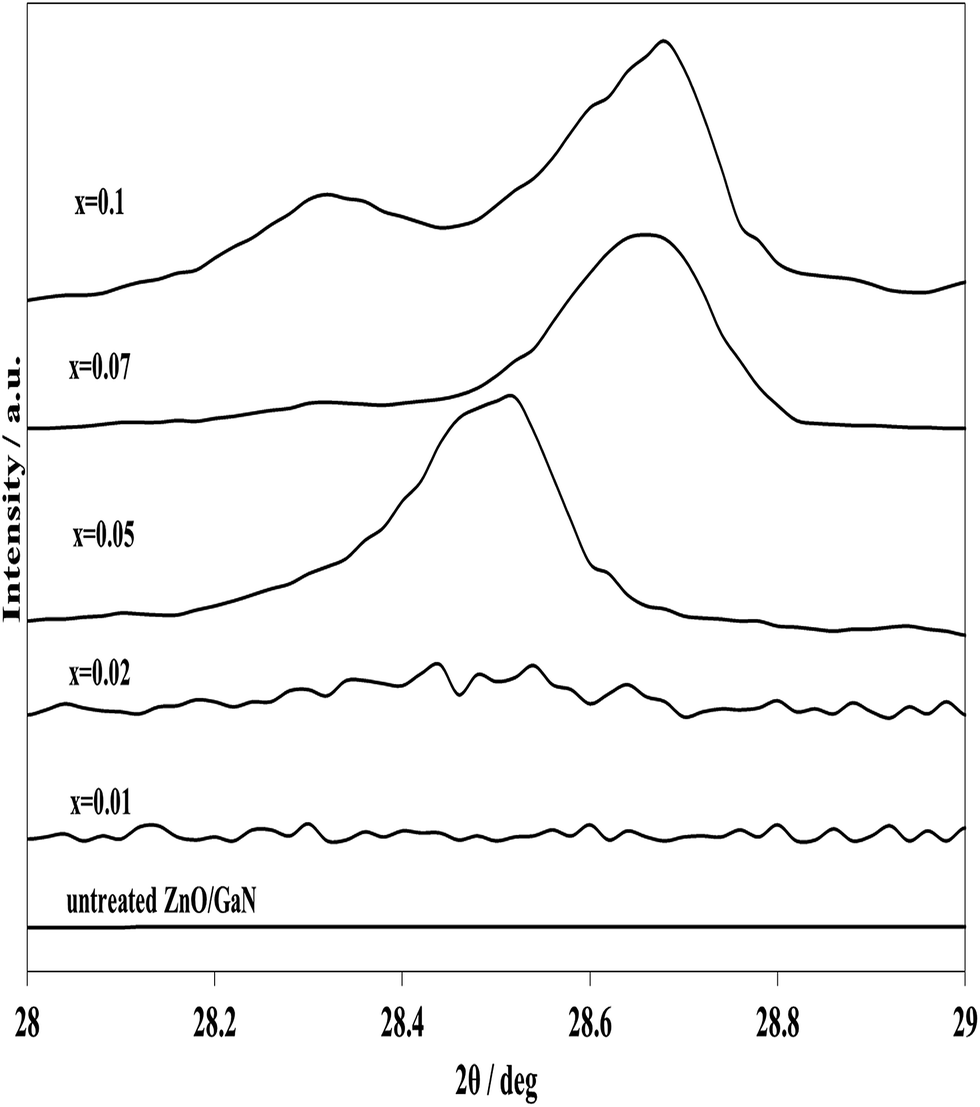 | ||
| Fig. 6 X-ray diffraction patterns in the range of 2θ = 28–29° for ZnO/GaN-P (873, x) with an x value in the range of 0.01 to 0.1 and untreated ZnO/GaN. | ||
Fig. 7 shows the X-ray diffraction patterns of ZnO/GaN-P (823, 0.07) at different phosphidation times. A single peak appeared at 2θ = 28.62° upon heating for 7 h. The peak increased in size at 14 h, and shifted slightly to a lower diffraction angle by 0.07° at 21 h. A very slight shift to a lower diffraction angle occurred with 28 h of phosphidation. To visualize the active structures, the photocatalytic activity obtained under various conditions such as different phosphidation temperatures, time and P amounts was consolidated and plotted against diffraction peak positions due to GaP in the range 2θ = 28–29°. As shown in Fig. 8, the photocatalytic activity at 823 K increased as the diffraction angle increased from 2θ = 28.32° (GaP crystal), producing a maximum at approximately 2θ = 28.6°, and decreases with further increase in the diffraction angle. A similar trend can be seen for 873 K phosphidation.
 | ||
| Fig. 7 X-ray diffraction patterns in the range of 2θ = 28–29° for ZnO/GaN-P (823, 0.07) at different phosphidation times from 7 to 28 h and untreated ZnO/GaN. | ||
 | ||
| Fig. 8 Photocatalytic activity vs. diffraction peak angles of GaP produced by phosphidation. The diffraction peak angle of normal GaP is shown for comparison. The photocatalytic activity for H2 production only was shown for simplicity. Numbers in figure shows the molar percentage of P added to ZnO/GaN and the time for phosphidation. No expression of time means 14 h phosphidation. Open and filled triangles: ZnO/GaN phosphidated at 823 K. Open rhombus: at 873 K. Open square: at 1073 K. Filled circle: normal GaP. | ||
These correlations demonstrate that a high photocatalytic activity depends on the structures of GaP1−xNx formed through the gas–solid reaction between vaporized P and GaN. To determine the active conformation, the diffraction peak shifts were simulated by taking the geometry optimized model of the GanPn−yNy into account. Fig. 9 shows the GaP diffraction peaks calculated by the powder diffraction method as implemented in the Reflex Module of the Dassault Systemes BIOVIA method for n = 32 and y = 1, 3, 4, 6, 7 and 8. A 2θ range of 10 to 90° was used with a step size of 0.05. Peak position errors can result from an incorrect zero point or from errors in the placement or transparency of the sample. In this case we have used Bragg–Brentano correction.36 A peak due to Ga32P32 appeared at 2θ = 27.65°, shifted to a higher angle with increasing N atom content, and attained at 2θ = 28.44° for y = 4, 2θ = 28.75° for y = 6 and 2θ = 29.03° for y = 8. The diffraction angle shifts against the percentage of P atoms in the total of P and N atoms P/(P + N) × 100% showed a good linear relationship (ESI Fig. S3†). In comparison with the experimental value which provides the greatest photocatalytic activity for shifts by 2θ = 0.20–0.44° to a higher diffraction angle from GaP (Fig. 8), the linear relationship provided the result that the optimal conditions for the highest activity are the involvement of N at the percentage of 3.4–7.4% in GaP.
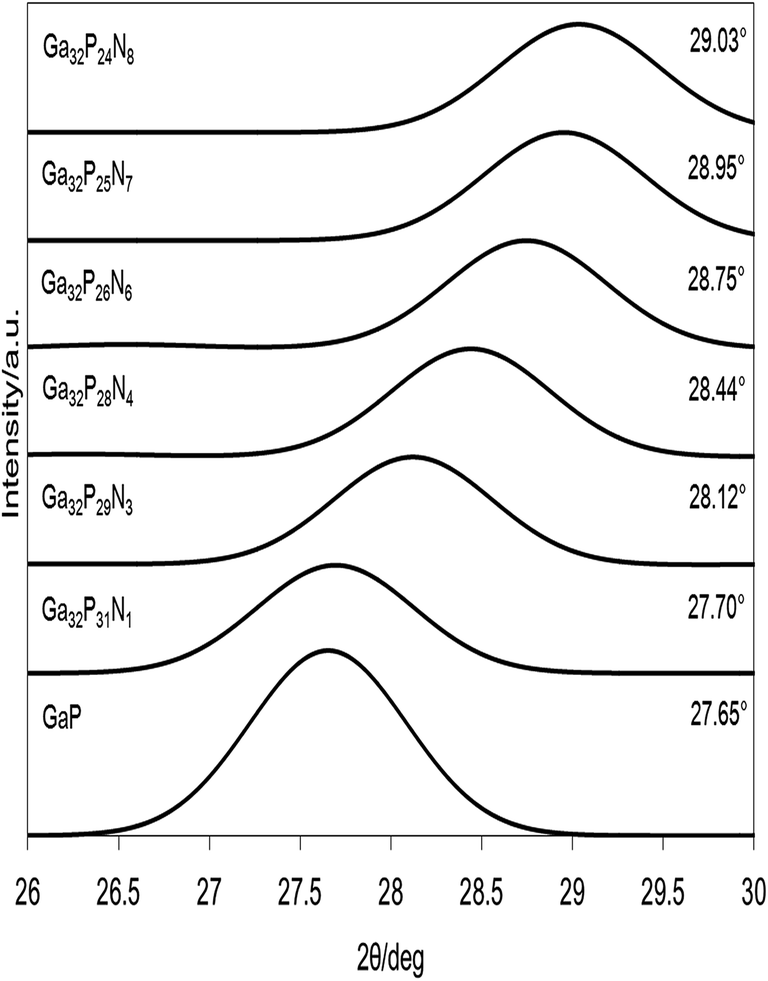 | ||
| Fig. 9 Simulated X-ray diffraction peaks of GaP for Ga32P32−yNy (y = 1–8). | ||
In order to see the electronic contribution of N atom in GaP, the density of states (DOS) was calculated by a DFT method assuming a super cell of Ga32P31N1 (the inclusion of the ZnO component caused a complexity in calculation, and its contribution is ignored here). Fig. 10 shows the total DOS and atom orbital (AO)-projected DOS (AO-PDOS). The occupied bands appearing with increasing energy consist of a sharp Ga 3d AO at around −14 eV, P 3s AO at around −10 eV, and the valence band, in which the lower energy part is mainly due to Ga 4s + P 3p + N 2p orbitals. The HOMO is composed of Ga 4p + P 3p + N 2p AOs. In the unoccupied bands, LUMO consists of Ga 4s4p + P 3p + N 2s AOs. The band gap is estimated to be 0.793 eV.
 | ||
| Fig. 10 Density of states for a Ga32P32N1 model cluster. In AO-PDOS of N, P and Ga atoms, solid line (—) is for s orbital, dash line (------) for p orbital, and alternate long and short dash line(— - — -) for d orbital. Total DOS is shown with a solid line. | ||
Discussion
The phosphidation of ZnO/GaN increased the photocatalytic activity for water splitting by a factor of 6–8. The quantum efficiency was estimated to be in the range 1–2% from comparison with photocatalytic activity previously obtained for RuO2–ZnO/GaN without phosphidation.4,5 The phosphidation conditions are restricted in a very narrow range in temperatures and the P amounts introduced, which indicates that the activation is very sensitive to the ratio of P to N. The appearance of new GaP peaks with higher X-ray diffraction angles, different from GaP crystal, is apparently associated with the photocatalyst activation. No shifts of GaP diffraction peaks in the inactive nitrided GaP (ESI Fig. S1†) are in line with this view. The simulation for the relationship of N contents vs. diffraction shifts (ESI Fig. S3†) showed that the high photocatalyst activation occurred at 3.4–7.4% of N concentrations in GaP. It should be noted that a small amount of N atoms in GaP is effective for the activation of GaP surfaces.GaP and GaN have a zinc blende and wurtzite structure, respectively. The differences in the crystal structures and lattice constant (∼20%) produce a large miscibility gap.37 Thus, in the growth of GaP1−xNx alloys, the N concentration was usually restricted below 1 × l019 cm−3 or 0.04%, but recently it was increased to as high as 3.1–7.6% in GaP1−xNx films epitaxially grown by MOVPE16 and molecular beam epitaxy (MBE).17–20,22 The introduction of N in GaP is a heavy isoelectric doping that has band effects. Photoluminescence (PL) measurements16–19,22 and theoretical calculations23–27 showed that the very limited N concentration of <1017 cm−3 produced an A-line due to the isolated N atom, and in the N concentration increasing up to ∼1019 cm−3, different NNi (i < 10) pairs were formed below the band gap. The concentration is not enough to change the potential of the band edge. However, the NNi pairs produce isoelectronic traps in the band and bind the electrons,13 which might be useful for photoexcited charge separation. At a higher N concentration of >0.5%, a band formed by N atoms merged the conduction band edges of GaP. Thus, the N atom concentration obtained in the present study is considered to contribute to the conduction band formation. This is confirmed from the DOS calculation for a model of Ga32P31N1 (3.1% N) that provided the conduction bands of hybridized Ga 4s4p + P 3p + N 2s AOs.
A maximum was observed in the relationship of photocatalytic activity against GaP peak shifts (Fig. 8). As phosphidation progressed, larger shifts of the GaP diffraction peak occurred, and also the diffraction peak assigned to the original GaP crystal appeared, as shown in Fig. 6. Thus, the photocatalytic activity that decreases with larger diffraction peak shifts are due to not only the dilution of N atom concentrations but the formation of inactive GaP phases.
The UV-Vis diffuse reflectance spectrum showed that the light absorbing wavelength of ZnO/GaN-P was slightly (∼7 nm) shorter than that of ZnO/GaN, opposite to those reported for the formation of the GaP1−xNx phase, in which the N atom inclusion in GaP caused shifts to a longer wavelength. The present ZnO/GaN system had characteristics of absorbing longer wavelength light than GaN, because of the solid solution effects of ZnO.10,38 It seems likely that the partial removal of the ZnO component from ZnO/GaN surfaces during phosphidation in vacuum has larger effects than the phosphidation, which results in the light absorption edge shifts to shorter wavelengths.
The band edges of GaP1−xNx/GaP(x = 0–0.035) were previously reported to be negative by more than 300 mV.28 This might be associated with the structures of thin films grown in mismatch between the GaP1−xNx film and substrate GaP. The flat band potentials of GaP at pH = 0 are in the range of 1.2–0.93 V,39 and thus the band edge for the oxidation of water is negative or very slightly positive, which makes it difficult for water splitting to proceed efficiently. On the other hand, ZnO/GaN has a valence band level considerably lower than the water oxidation level. The valence bands of ZnO/GaN-P consist of the hybridized Ga 4p + P 3p + N 2p AOs, which forms intermediate electronic band structures of GaP and GaN. Thus, the N atom inclusion to GaP lowers the valence band edge enough for the oxidation to proceed. This has positive effects on the oxidation of water, although the conduction band edge shifts to a lower energy level. The disadvantage of not only GaP but possibly many metal phosphides is the valence band edge being higher than or nearly the same as the oxidation level of water. Schematic band structures and energy levels are schematically depicted in Fig. 11. The presented results indicate that the consolidation of metal phosphides with N atoms is able to extend the availability of meal phosphides to photocatalysts for water splitting.
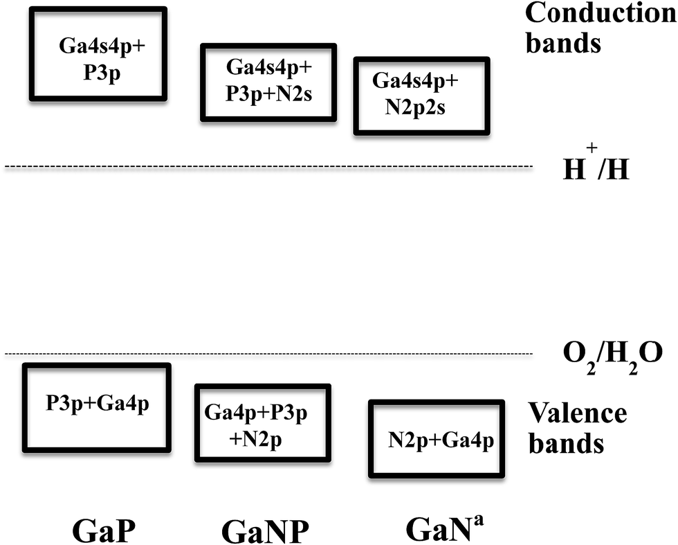 | ||
| Fig. 11 Schematic band structures and energy levels of GaP, GaNP and GaN. aIndicates result from ref. 1. | ||
In conclusion, the phosphidation of active ZnO/GaN photocatalysts significantly enhances the photocatalytic activity for water splitting. The phosphidation of ZnO/GaN successfully permits to achieve optimal nitrogen conditions in GaP1−xNx, which leads to the generation of high photocatalytic performance. The present approach shows promise for application to other metal nitride systems that will be advantageous for efficient photocatalysts for water splitting.
Acknowledgements
Financial support from INPEX is gratefully appreciated.References
- N. Arai, N. Saito, H. Nishiyama, K. Domen, H. Kobayashi, K. Sato and Y. Inoue, Catal. Today, 2007, 129, 407–413 CrossRef CAS PubMed.
- N. Arai, N. Saito, H. Nishiyama, Y. Inoue, K. Domen and K. Sato, Chem. Lett., 2006, 35, 796–797 CrossRef CAS.
- K. Maeda, T. Takata, M. Hara, N. Saito, Y. Inoue, H. Kobayashi and K. Domen, J. Am. Chem. Soc., 2005, 127, 4150–4151 CrossRef PubMed.
- K. Teramura, K. Maeda, T. Saito, T. Takata, N. Saito, Y. Inoue and K. Domen, J. Phys. Chem. B, 2005, 109, 21915–21921 CrossRef CAS PubMed.
- K. Maeda, K. Teramura, T. Takata, M. Hara, N. Saito, K. Toda, Y. Inoue, H. Kobayashi and K. Domen, J. Phys. Chem. B, 2005, 109, 20504–20510 CrossRef CAS PubMed.
- K. Maeda, K. Teramura, D. Lu, T. Takata, M. Hara, N. Saito, Y. Inoue and K. Domen, Nature, 2006, 440, 295 CrossRef CAS PubMed.
- K. Maeda, K. Teramura, H. Masuda, T. Takata, N. Saito, Y. Inoue and K. Domen, J. Phys. Chem. B, 2006, 110, 13107–13112 CrossRef CAS PubMed.
- K. Maeda, K. Teramura, N. Saito, Y. Inoue and K. Domen, J. Catal., 2006, 243, 303–308 CrossRef CAS PubMed.
- K. Maeda, K. Teramura, D. Lu, N. Saito, Y. Inoue and K. Domen, J. Phys. Chem. C, 2007, 111, 7554–7560 CAS.
- M. Yoshida, T. Hirai, K. Maeda, N. Saito, J. Kubota, H. Kobayashi, Y. Inoue and K. Domen, J. Phys. Chem. C, 2010, 114, 15510–15515 CAS.
- J. R. Chelikowsky and M. L. Cohen, Phys. Rev. B, 1976, 14, 556–582 CrossRef CAS.
- C. S. Wang and B. M. Klein, Phys. Rev. B, 1981, 24, 3393–3416 CrossRef CAS.
- D. G. Thomas and J. J. Hopfield, Phys. Rev., 1966, 150, 680–689 CrossRef CAS.
- E. Cohen and M. D. Sturge, Phys. Rev. B, 1977, 15, 1039–1051 CrossRef CAS.
- S. Miyoshi, H. Yaguchi, K. Onabe, R. Ito and Y. Shiraki, Appl. Phys. Lett., 1993, 63, 3506–3508 CrossRef CAS PubMed.
- H. Yaguchi, S. Miyoshi, G. Biwa, M. Kibune, K. Onabe, Y. Shiraki and R. Ito, J. Cryst. Growth, 1997, 170, 353–356 CrossRef CAS.
- Y. Zhang, B. Fluegel, A. Mascarenhas, H. P. Xin and C. W. Tu, Phys. Rev. B, 2000, 62, 4493–4500 CrossRef CAS.
- W. Shan, W. Walukiewicz, K. M. Yu, J. Wu, J. W. Ager III, E. E. Haller, H. P. Xin and C. W. Tu, Appl. Phys. Lett., 2000, 76, 3251–3253 CrossRef CAS PubMed.
- H. P. Xin, C. W. Tu, Y. Zhang and A. Mascarenhas, Appl. Phys. Lett., 2000, 76, 1267–1269 CrossRef CAS PubMed.
- G. Y. Rudko, I. A. Buyanova, W. M. Chen, H. P. Xin and C. W. Tu, Appl. Phys. Lett., 2002, 81, 3984–3986 CrossRef CAS PubMed.
- C. V. Reddy, R. E. Martinez II, V. Narayanamurti, H. P. Xin and C. W. Tu, Phys. Rev. B, 2002, 66, 235313-1–235313-4 CrossRef.
- J. N. Baillargeon, K. Y. Cheng, G. E. Hofler, P. J. Pearah and K. C. Hsieh, Appl. Phys. Lett., 1992, 60, 2540–2542 CrossRef CAS PubMed.
- R. A. Faulkner and P. J. Dean, J. Lumin., 1970, 1–2, 552–561 CrossRef.
- B. Gil, J. P. Albert, J. Camassel, H. Mathieu and B. C. Guillaume, Phys. Rev. B, 1986, 33, 2701–2712 CrossRef CAS.
- L. Bellaiche, Su-H. Wei and A. Zunger, Phys. Rev. B, 1997, 56, 10233–10240 CrossRef CAS.
- P. R. C. Kent and A. Zunger, Phys. Rev. Lett., 2001, 86, 2613–2616 CrossRef CAS.
- P. R. C. Kent and A. Zunger, Phys. Rev. B, 2001, 64, 115208-1–115208-23 CrossRef.
- T. G. Deutsch, C. A. Koval and J. A. Turner, J. Phys. Chem. B, 2006, 110, 25297–25307 CrossRef CAS PubMed.
- M. C. Payne, M. P. Teter, D. C. Allan, T. A. Arias and J. D. Johannopoulos, Rev. Mod. Phys., 1992, 64, 1045–1097 CrossRef CAS.
- D. Vanderbilt, Phys. Rev. B, 1990, 41, 7892–7895 CrossRef.
- S. J. Clark, M. D. Segall, C. J. Pickard, P. J. Hasnip, M. I. J. Probert, K. Refson and M. C. Payne, Z. Kristall, 2005, 220, 567–570 CrossRef CAS.
- J. P. Perdew and A. Zunger, Phys. Rev. B, 1981, 23, 5048–5079 CrossRef CAS.
- J. P. Perdew, Phys. Rev. B, 1986, 33, 8822–8824 CrossRef.
- A. D. Becke, Phys. Rev. A, 1988, 38, 3098–3100 CrossRef CAS.
- H. J. Monkhorst and J. D. Pack, Phys. Rev. B, 1976, 13, 5188–5192 CrossRef.
- A. J. C. Wilson, Mathematical Theory of X-ray Powder Diffraction, Philips Technical Library, Eindhoven, 1963 Search PubMed.
- G. B. Stringfellow, J. Electrochem. Soc., 1972, 119, 1780–1782 CrossRef CAS PubMed.
- L. L. Jensen, J. T. Muckerman and M. D. Newton, J. Phys. Chem. C, 2008, 112, 3439–3446 CAS.
- G. Horowitz, J. Appl. Phys., 1978, 49, 3571–3573 CrossRef CAS PubMed.
Footnote |
| † Electronic supplementary information (ESI) available: Full description of the material. See DOI: 10.1039/c5ta04732c |
| This journal is © The Royal Society of Chemistry 2015 |