
 Open Access Article
 This Open Access Article is licensed under a Creative Commons Attribution-Non Commercial 3.0 Unported Licence
Solution-processed inorganic copper(I) thiocyanate (CuSCN) hole transporting layers for efficient p–i–n perovskite solar cells†
K.
Zhao
,
R.
Munir
,
B.
Yan
,
Y.
Yang
,
T.
Kim
and
A.
Amassian
*
Materials Science and Engineering, Division of Physical Sciences and Engineering, Solar and Photovoltaics Engineering Research Center (SPERC), King Abdullah University of Science and Technology (KAUST), Thuwal 23955-6900, Saudi Arabia. E-mail: aram.amassian@kaust.edu.sa
First published on 27th August 2015
Abstract
CuSCN is a highly transparent, highly stable, low cost and easy to solution process HTL that is proposed as a low cost replacement to existing organic and inorganic metal oxide hole transporting materials. Here, we demonstrate hybrid organic–inorganic perovskite-based p–i–n planar heterojunction solar cells using a solution-processed copper(I) thiocyanate (CuSCN) bottom hole transporting layer (HTL). CuSCN, with its high work function, increases the open circuit voltage (Voc) by 0.23 V to 1.06 V as compared with devices based on the well-known poly(3,4-ethylenedioxythiophene)![[thin space (1/6-em)]](https://www.rsc.org/images/entities/char_2009.gif) :poly(styrenesulfonate) (PEDOT:PSS) (0.83 V), resulting in a superior power conversion efficiency (PCE) of 10.8% without any notable hysteresis. Photoluminescence measurements suggest a similar charge transfer efficiency at the HTL/perovskite interface to PEDOT:PSS. However, we observe more efficient light harvesting in the presence of CuSCN at shorter wavelengths despite PEDOT:PSS being more transparent. Further investigation of the microstructure and morphology reveals differences in the crystallographic texture of the polycrystalline perovskite film, suggesting templated perovskite growth on the surface of CuSCN. The successful demonstration of the solution-processed inorganic HTL using simple and low temperature processing routes bodes well for the development of reliable and efficient flexible p–i–n perovskite modules or for integration as a front cell in hybrid tandem solar cells.
:poly(styrenesulfonate) (PEDOT:PSS) (0.83 V), resulting in a superior power conversion efficiency (PCE) of 10.8% without any notable hysteresis. Photoluminescence measurements suggest a similar charge transfer efficiency at the HTL/perovskite interface to PEDOT:PSS. However, we observe more efficient light harvesting in the presence of CuSCN at shorter wavelengths despite PEDOT:PSS being more transparent. Further investigation of the microstructure and morphology reveals differences in the crystallographic texture of the polycrystalline perovskite film, suggesting templated perovskite growth on the surface of CuSCN. The successful demonstration of the solution-processed inorganic HTL using simple and low temperature processing routes bodes well for the development of reliable and efficient flexible p–i–n perovskite modules or for integration as a front cell in hybrid tandem solar cells.
1. Introduction
Organometallic halide perovskite materials, first investigated in photovoltaic devices by Kojima et al.,1 have been studied intensively due to their large absorption coefficient, high carrier mobility and diffusion length.2,3 Recently, the power conversion efficiency (PCE) of perovskite solar cells has surpassed 20% both in mesoscale and planar heterojunction architectures.4 To date, much of this progress has been made in the n–i–p architecture employing a planar or mesoporous (mp) metal oxide as an electron transporting layer (ETL), and spiro-MeOTAD as a hole transporting layer (HTL). The ETL and HTL promote the selective extraction of electrons and holes to the cathode and anode, respectively. Perovskite solar cells based on the p–i–n planar heterojunction, in which the substrate to the perovskite layer is poly(3,4-ethylenedioxythiophene) poly(styrenesulfonate) (PEDOT:PSS) as the HTL and [6,6]-phenyl-C61-butyric acid methylester (PCBM) is used as the ETL, are the most successful and popular implementations of the p–i–n architecture.5,6 This architecture is reminiscent of standard organic solar cells and has great potential for low temperature fabrication of standalone solar cells on plastics or as front cells in hybrid tandem devices.7 However, PEDOT:PSS is difficult to synthesize, costly and its acidic and hygroscopic characteristics can cause indium loss from the indium tin oxide (ITO) transparent anode, adversely affecting the device stability.8,9 Recent studies also suggest that the electron blocking properties of PEDOT:PSS may be insufficient given its semi-metallic nature.10
Solution-processed inorganic p-type semiconductors have been proposed as alternatives to PEDOT:PSS owing to their relatively low cost, greater stability and potential for implementation in a hybrid tandem structure. Nickel oxide (NiOx) has been successfully used as an efficient hole collecting interlayer in p–i–n perovskite solar cells. Hu et al. presented the device architecture of ITO/spin-coated NiOx/sequentially deposited CH3NH3PbI3/PCBM/Al with a UV-ozone treatment to achieve a device PCE of 7.6%.11 With further improvement in the quality of the NiOx film, the device performance has been significantly improved to 15.4% via substitutional Cu doping.12–14 Solution-processed pseudohalides, such as copper iodide (CuI) and copper thiocyanate (CuSCN), have recently emerged as other effective and robust p-type inorganic semiconductors which can achieve high quality ordered thin films even from room temperature processing.15–17 CuSCN is a highly transparent intrinsically p-type semiconductor which has also been shown to work effectively in transparent electronic devices15–17 and as an efficient HTL in organic solar cells.18,19 A CuSCN layer with 600–700 nm thickness was successfully used as a low-cost replacement for spiro-OMeTAD in conventional n–i–p planar and mesostructured perovskite solar cells achieving PCE as high as 12.4%.20,21 Very recently, Ye et al. fabricated high-quality perovskite films on top of a rough CuSCN layer using a one-step formation method, resulting in highly efficient planar p–i–n perovskite solar cells.22 However, the CuSCN layer was fabricated via electro-deposition, which required careful synthesis from an aqueous solution containing copper sulfate (CuSO4), ethylenediaminetetraacetic acid (EDTA) and potassium thiocyanate (KSCN).
Herein, we show that thin and smooth CuSCN films can be easily solution processed at low temperature (60 °C) and used effectively as bottom HTLs in planar heterojunction p–i–n perovskite solar cells. Perovskite solar cells consistently show a PCE of 10.8% with negligible hysteresis. This marks a substantial increase from that of the control p–i–n solar cell using PEDOT:PSS as the HTL and is mainly attributed to a substantial increase of the Voc by 0.23 V, which comes from more favorable energetics at the CuSCN/CH3NH3PbI3 interface. To our surprise, we found that the external quantum efficiency in the highly transparent window of CuSCN to be lower than that in the control device. We have investigated the microstructure of the perovskite film and presented evidence to the effect that perovskite texture may be altered by the CuSCN layer. The successful implementation of a highly facile, solution-processed CuSCN film as the bottom HTL in p–i–n perovskite solar cells shows a successful alternative to organic and metal oxide semiconductors currently being explored as HTLs for perovskite solar cells.
2. Results and discussion
2.1 Microstructure, optical and electronic properties of CuSCN thin films
Thin films of CuSCN were deposited onto cleaned ITO substrates via spin coating a solution at room temperature, followed by annealing at 60 °C for 2 minutes to remove the excess solvent. Transmission electron micrographs (TEM) (Fig. 1a) of the prepared CuSCN layer (∼13 nm) reveal a continuous and pin hole-free film with densely packed rod-like crystals. The crystals have a width in the range of 30–40 nm and vary in length between 60 and 100 nm. High resolution TEM (Fig. 1b) images show clear lattice fringes proving the material's crystallinity. The Fast Fourier Transform (FFT) spectral image taken for the selected area indicates a d-spacing of 0.27 nm, corresponding to the crystalline structure of both the hexagonal/rhombohedral β-phase and the orthorhombic α-phase as we have discussed in a previous study.16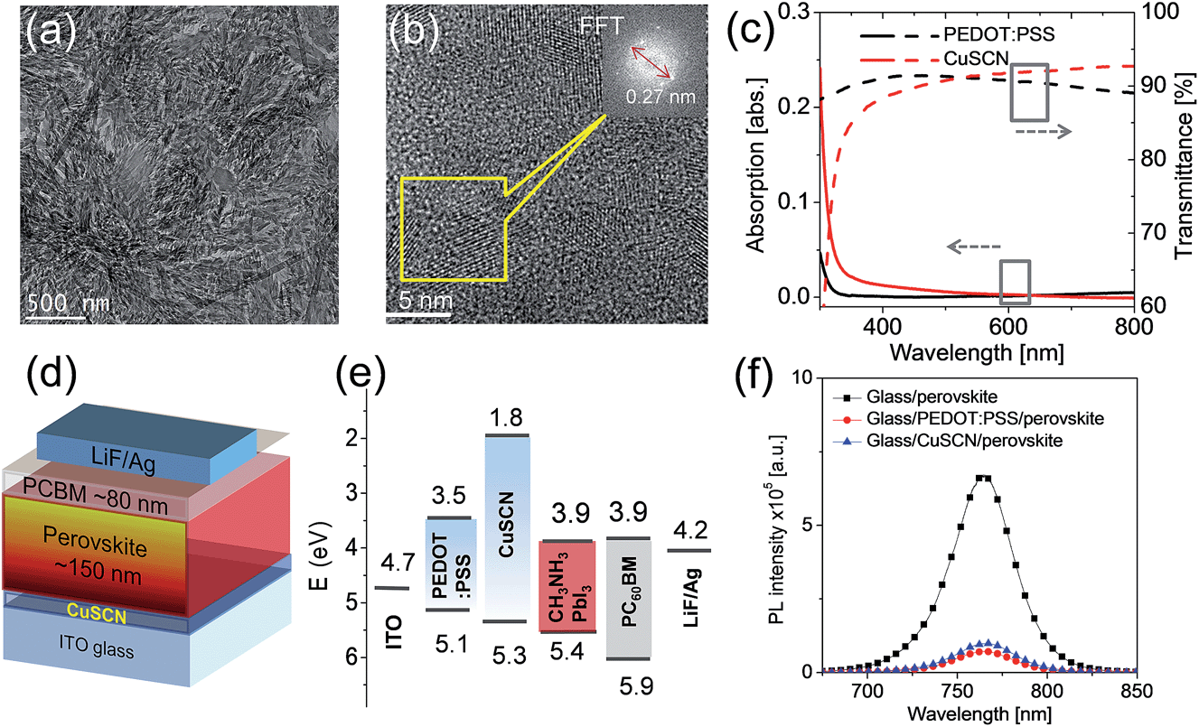 | ||
| Fig. 1 (a) A transmission electron micrograph (TEM) of the solution-processed CuSCN film. (b) The high-resolution TEM image of a CuSCN crystal and associated FFT shown in the inset. (c) Absorption spectra and transmittance of 30 nm-thick PEDOT:PSS and 13 nm-thick CuSCN films. (d) Schematic of the p–i–n solar cell architecture used in this study. (e) The energy level diagram of the CuSCN/perovskite/PC60BM p–i–n heterojunction. (f) Steady-state photoluminescence spectra showing similarly strong quenching of the perovskite emission on both PEDOT:PSS and CuSCN HTLs. | ||
As optical transparency is a key parameter for the HTL in the p–i–n architecture with bottom illumination, we have plotted in Fig. 1c the absorption spectra and transmittance of the solution-processed CuSCN film (∼13 nm) deposited directly on a glass substrate. Since PEDOT:PSS is the most used HTL in p–i–n perovskite solar cells, the transmission and absorption spectra of a PEDOT:PSS layer (∼30 nm) on glass are also shown for comparison. The result shows an onset of absorption of the CuSCN film at ca. 320 nm. The CuSCN film exhibits high transparency (>90%) in the wavelength region above 450 nm and slightly lower for the rest of the lower wavelength region (60% at 300 nm). While the transmittance is comparatively lower for CuSCN than PEDOT:PSS in the ultraviolet region, CuSCN is more transparent than PEDOT:PSS above 520 nm.
Solution-processed CuSCN films can be used as effective bottom HTLs in perovskite-based p–i–n junction solar cells according to the energy level diagram shown in Fig. 1e for the device structure of ITO/CuSCN/CH3NH3PbI3/PC60BM/LiF/Ag (Fig. 1d). The energy levels of CuSCN were determined from ultraviolet photoelectron spectroscopy (UPS) and optical measurements of the band gap and are in agreement with a previous report.15 We observe more favorable energetics for the CuSCN based device structure as compared to PEDOT:PSS. The valence band edge is 5.3 eV for CuSCN, a full 0.2 eV higher than the HOMO of PEDOT:PSS, and 5.4 eV for the CH3NH3PbI3 film. This arrangement is expected to increase the Voc commensurately if the charge injection from the perovskite to CuSCN is efficient.13
Hole injection from the photoexcited perovskite into CuSCN is investigated via photoluminescence (PL) quenching measurements of the CH3NH3PbI3 emission for films grown on CuSCN and on PEDOT:PSS (Fig. 1f). PEDOT:PSS has been reported to strongly quench perovskite emission, suggestive of this being an effective p-type contactor capable of good hole injection at the HTL-perovskite interface.23 We observe similarly strong PL quenching of the perovskite emission on both PEDOT:PSS and CuSCN as compared to the perovskite grown directly on glass, implying that charge transfer occurs efficiently at the CuSCN–perovskite interface. Based on the thin film microstructure and properties presented herein, it is expected that solution-processed CuSCN should work well as a HTL in p–i–n perovskite solar cells as it does in n–i–p devices.
2.2 Photovoltaic performance
In Fig. 2, we show the current–voltage (J–V) characteristics measured with a scan rate of 0.1 V s−1 under AM 1.5G (100 mW cm−2) irradiation for the devices comprised of ITO/CuSCN (or PEDOT:PSS)/CH3NH3PbI3/PC60BM/LiF/Ag. The device figures of merit are summarized in Table 1. A reference cell based on the PEDOT:PSS HTL delivers an average short circuit current density (Jsc) of 16.8 mA cm−2, an open-circuit voltage (Voc) of 0.83 V, a fill factor (FF) of 70.1% and an overall PCE of 9.7%. The device based on CuSCN displays better overall performance in comparison to PEDOT:PSS under the same conditions, reaching a PCE of 10.8%, thanks mainly to an increased Voc to 1.06 V, although the other parameters decreased slightly: Jsc = 15.7 mA cm−2 and FF = 64.9% (Fig. 2a) The efficient photovoltaic performance confirms our previous assertions about the excellent quality of CuSCN as a HTL for p–i–n perovskite solar cells. The improvement of the Voc by 0.23 V with respect to the PEDOT:PSS device is quite remarkable and could be explained by the energetic differences at the perovskite/HTL interface. A similar observation of Voc enhancement was reported in organic solar cells when replacing PEDOT:PSS by CuSCN,19 which was attributed to better interfacial energy alignment between the donor and CuSCN. The Jsc of the CuSCN-based cell was found to be lower than that expected. The external quantum efficiency (EQE) is evaluated in Fig. 2b for clues; it shows a lower intensity in the wavelength range from 600 to 720 nm but a higher intensity in the region of 430 to 620 nm for the CuSCN based cell compared to the PEDOT:PSS based cell, exactly the opposite of the expected trend based on Fig. 1c. Absorption spectra of the perovskite/CuSCN and perovskite/PEDOT:PSS stacks show no difference (Fig. S1†), indicating that the origin of the EQE differences might stem from other factors. The dark J–V curve shown in Fig. S2† presents a slightly lower leakage current density and a higher rectification ratio for the device based on CuSCN in comparison to PEDOT:PSS HTL, suggesting a possibility of reduced recombination at the CuSCN–perovskite interface.
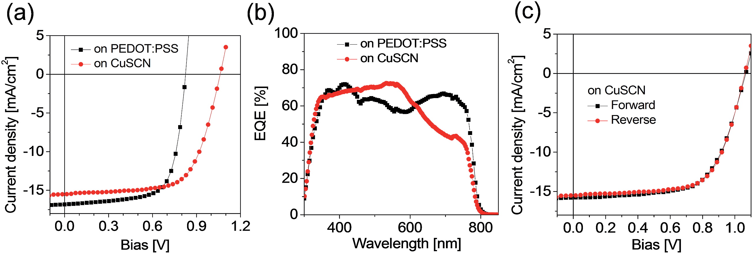 | ||
| Fig. 2 (a) The current–voltage characteristics and (b) external quantum conversion efficiency (EQE) spectra of photovoltaic devices made of ITO/CuSCN (or PEDOT:PSS)/CH3NH3PbI3/PC60BM/LiF/Ag. (c) J–V curves of solar cells based on the CuSCN HTL with forward and reverse scanning directions. The dark J–V curves are shown in Fig. S2.† | ||
:PSS and CuSCN as bottom HTLs. The results are expressed in terms of the average and standard deviation from over 5 devices
| HTL | Scan direction | J sc [mA cm−2] | V oc [V] | FF [%] | PCEave (PCEmax) [%] | Calculated Jsc [mA cm−2] |
|---|---|---|---|---|---|---|
| PEDOT:PSS |
Forward | 15.64 ± 0.17 | 0.83 ± 0.00 | 68.8 ± 0.42 | 9.2 ± 0.15 (9.4) | 16.13 |
| Reverse | 16.32 ± 0.23 | 0.83 ± 0.00 | 69.5 ± 0.46 | 9.4 ± 0.18 (9.7) | ||
| CuSCN | Forward | 15.76 ± 0.02 | 1.06 ± 0.01 | 63.2 ± 0.52 | 10.5 ± 0.16 (10.8) | 15.02 |
| Reverse | 15.23 ± 0.26 | 1.06 ± 0.00 | 65.4 ± 0.40 | 10.5 ± 0.19 (10.8) |
We have also made a simple comparison of the lifetime of non-encapsulated solar cells based on PEDOT:PSS and CuSCN HTLs after being kept in a N2 environment (Fig. S3†). Encouragingly, the results indicate a comparatively slower decline of the overall device performance in the case of CuSCN versus the PEDOT:PSS HTL. The initial performance was maintained at 40% for the CuSCN-based device while 20% for the PEDOT:PSS device after 2 weeks. The relatively low stability of the PEDOT:PSS-based device could partially be attributed to the acidic and hygroscopic characteristics of PEDOT:PSS which cause indium loss from ITO.8,9
An anomalous hysteresis in the J–V curves of perovskite solar cells has been observed and intensely investigated in previous reports,24–26 where the hysteresis was explained to be significantly dependent on the p- and n-type contact materials and mesoporous versus planar structures. The J–V curves of solar cells based on PEDOT:PSS and CuSCN HTLs were tested using both the forward scan direction (from short circuit to bias) and the reverse scan direction at a scan rate of 0.1 V s−1 (Fig. 2c and Table 1). A PCE of 9.4% and 9.7% was recorded at forward and reverse scans for the PEDOT:PSS based cell, respectively, while both forward and reverse scans yielded a negligible variation in J–V characteristics for the CuSCN based cell, showing the same PCE of 10.8%. We have furthermore integrated the EQE spectra to extract the photocurrent and find excellent agreement within ±2%, as shown in Table 1. This indicates that both forward and reverse scans provide an accurate representation of the cell's photovoltaic performance.
2.3 Perovskite structural morphology on CuSCN
In light of the unexplained spectral behavior of light harvesting, we investigated the microstructure of the perovskite film for possible hints. CuI was previously shown to modify the stacking behavior and polycrystalline texture of organic semiconductors.26 We have explored this possible scenario by comparing the morphology and microstructure of perovskite films formed on PEDOT:PSS and CuSCN. In Fig. 3, we illustrate scanning electron micrographs (SEMs) of the surface of the CH3NH3PbI3 film along with a cross-sectional view of the solar cells. The films cover the substrate completely and form closely connected grains ranging in size from 100 to 600 nm (Fig. 3a). The surface and cross-sectional morphologies appear to be very similar, but the perovskite film (155–160 nm thickness) on CuSCN seems to form a more densely packed film and a more abrupt interface (Fig. 3b).
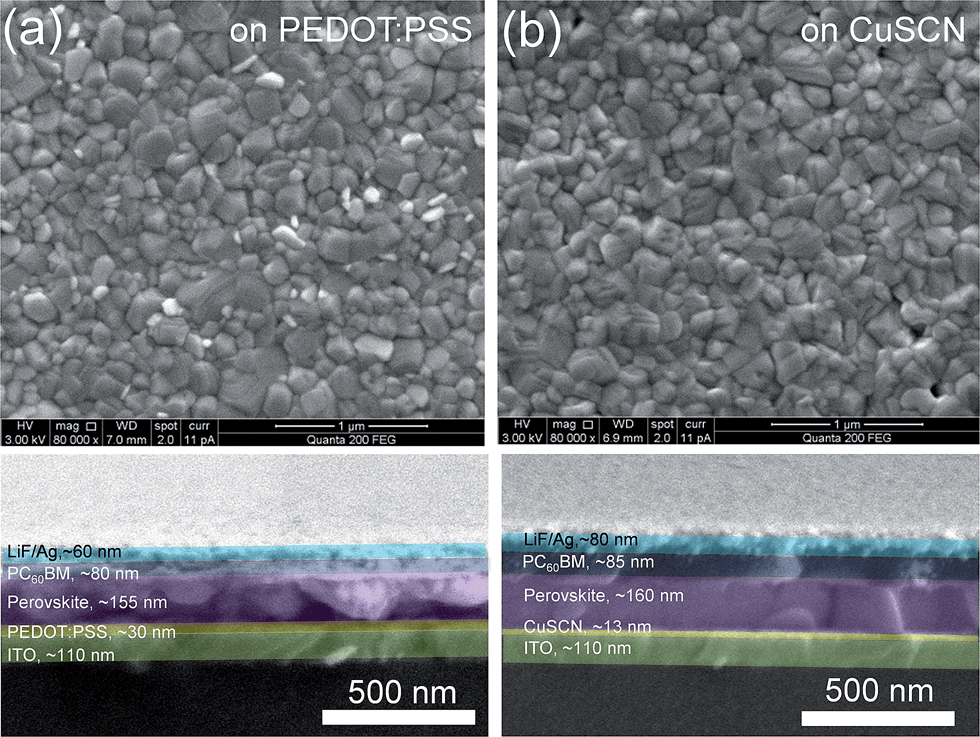 | ||
| Fig. 3 Plan-view SEM images of the CH3NH3PbI3 layer and the cross-sectional SEM images of a representative cell formed on (a) PEDOT:PSS and (b) CuSCN HTLs. | ||
In Fig. 4, we further evaluate the effect of the CuSCN HTL on the perovskite crystalline texture. The high resolution TEM images of the CH3NH3PbI3 films formed on CuSCN and PEDOT:PSS HTLs reveal the same d-spacing of 0.31 nm of lattice fringes of an individual perovskite grain, which correspond to the crystalline structure of (004) or (220) of the tetragonal CH3NH3PbI3 phase (Fig 4a and b).27 The XRD spectrum of CH3NH3PbI3 films on both HTLs exhibits quite similar XRD patterns at 14.1°, 28.7°, and 32.1° (Fig. 4c), which correspond to the (110), (220), and (310) planes, respectively.28 The observation of three sharp peaks confirms the high crystallinity of the CH3NH3PbI3 film on both CuSCN and PEDOT:PSS HTLs. Grazing incidence wide angle X-ray scattering (GIWAXS) profiles of crystalline CH3NH3PbI3 thin films on both HTLs show the scattering rings at q = 10 nm−1, which is assigned to the (110) plane of the CH3NH3PbI3 structure.29 The strong scattering rings indicate that perovskite domains are predominantly polycrystalline (Fig. 4d and e). Meanwhile we did not observe the scattering peak of PbI2 at q = 9 nm−1, indicating full conversion of MAI:PbI2 precursors to perovskite crystals on both HTLs. However we found that replacement of PEDOT:PSS by CuSCN does affect crystal orientation. We integrate the intensity of the q = 10 nm−1 peak and plot it vs. the azimuthal angle in Fig. 4f. The integration exhibits a preferred texture at 90° for a significant fraction of the perovskite crystallites grown on CuSCN that is different from PEDOT:PSS, where there is a 45–50° texture. This is not a huge texture difference, but a mild one which might suggest intriguingly that CuSCN may have a templating effect on perovskite crystallization. Whether such a change in texture should impact solar cell performance is not clear and remains speculative. It will require more experimental and theoretical investigations which are outside the scope of this study.
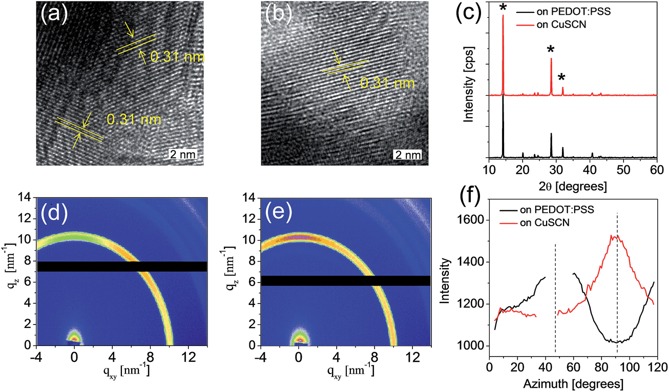 | ||
| Fig. 4 (a and b) The high resolution TEM images of the CH3NH3PbI3 films on PEDOT:PSS and CuSCN HTLs, respectively. (c) XRD spectra showing the same crystalline structure of the CH3NH3PbI3 films on both PEDOT:PSS and CuSCN HTLs. (d and e) Grazing incidence wide angle X-ray scattering (GIWAXS) profiles showing polycrystalline CH3NH3PbI3 on both PEDOT:PSS and CuSCN HTLs, respectively. (f) The azimuthal-angle intensity of the q = 10 nm−1 peak from GIWAXS for perovskite thin-films on both HTLs showing different preferred orientations of texture. | ||
3. Summary
In conclusion, a methylammonium lead iodide (CH3NH3PbI3) perovskite p–i–n junction solar cell is developed based on CuSCN as the bottom HTL to achieve excellent power conversion efficiency of 10.8% with a negligible hysteresis. The solar cells exhibit 1% higher PCE when using CuSCN than when PEDOT:PSS is used as the HTL, due in large part to a significant increase of the Voc by 0.23 V and despite a slight decrease of FF and Jsc. We also show that the replacement of the conventional PEDOT:PSS HTL by CuSCN did not change the charge transfer at the HTL/perovskite interface. A potential crystallization templating effect of CuSCN was observed which results in a different preferred texture of the perovskite crystal on the CuSCN HTL in comparison to that of PEDOT:PSS. In closing, CuSCN is a non-toxic, cost effective competitor, very easy to process at low temperature, making it a good candidate for the development of high performance perovskite-based p–i–n junction solar cells and potential design of tandem devices.
4. Experimental
4.1 Solution preparation and device fabrication
The solution preparation was conducted under an inert atmosphere inside a nitrogen glovebox. As-received CuSCN (Aldrich) was dissolved in dipropyl sulfide (Merck, 99% purity) at a concentration of 15 mg mL−1. The solution was left to stir for 5 h at room temperature and then filtered with 0.2 µm PVDF filters before spin-coating. Perovskite precursor solution, CH3NH3I (1-Material) and PbI2 (Aldrich) were dissolved in a mixed solvent of dimethylsulfoxide and γ-butyrolactone (4:6 in volume) in 1 M concentration. The solution was stirred overnight at 60 °C and filtered with a 0.2 µm PTFE filter before spin-coating. ITO/glass (15 Ω sq−1, ITO thickness 140 nm) substrates were cleaned through sequential sonication in sodium dodecyl sulfate (SDS) solution, deionized water, acetone and isopropanol for 15 min each. Substrate cleaning was completed through exposure to oxygen plasma for 10 min. The cleaned ITO/glass substrates were immediately spin coated with PEDOT:PSS (Clevious, AI4083) at 4000 rpm for 30 s in ambient atmosphere or moved to the nitrogen glovebox and spin coated with CuSCN with a thickness of ∼13 nm. The as-cast PEDOT:PSS films were then baked at 140 °C for 10 min in ambient atmosphere to dry water. The as-cast CuSCN films can be dried at 60 °C for 2 min to dry the solvent faster. The perovskite solution was coated onto the PEDOT:PSS or CuSCN substrates by a consecutive two-step spin-coating process at 1000 and 5000 rpm for 10 and 40 s, respectively. During the second step of spin-coating, chlorobenzene was dropped onto the substrate. The substrates were annealed at 100 °C for 5 minutes. After thermal annealing was finished, PC60BM (15 mg mL−1 in chlorobenzene) was then deposited by spin coating at 1000 rpm for 30 s. Finally, LiF (1 nm) and Ag (∼70 nm) electrodes were deposited by thermal evaporation. The active area of this electrode was fixed at 0.10 cm2. The current density–voltage characteristics of the photovoltaic cells were measured using a Keithley 2400 under simulated AM 1.5G solar irradiation at 100 mW cm−2. The external quantum efficiency (EQE) was recorded by using a Oriel Quantum Efficiency Measurement Kit (Newport).
4.2 Electron microscopy
A transmission electron microscope operating at 300 kV (Titan Cryo Twin, FEI Company, Hillsboro, OR) was used to acquire plan-view micrographs. Standard resolution SEM images were acquired using a LEO 1525 field emission scanning electron microscope at an operating voltage of 5 kV.4.3 Optical metrology
UV-visible transmission and absorption spectra were acquired on a Cary 5000 (Varian) instrument. Photoluminescence (PL) spectra were recorded in backscattering geometry on a LabRAM Aramis (Horiba Jobin Yvon) Raman spectrometer with 532 nm laser used as the excitation source. A 100× objective lens with a numerical aperture (N. A.) of 0.90 was used to focus the laser beam and collect scattered light. The typical acquisition time was 1 s, and the laser power was maintained at 0.006 mW to avoid the heating effect.Acknowledgements
The authors would like to thank Prof. Thomas D. Anthopoulos for useful discussion on solution processed CuSCN film. Part of this work was supported by the KAUST Office of Competitive Research under round 2 of the Competitive Research Grant.References
- A. Kojima, K. Teshima, Y. Shirai and T. Miyasaka, J. Am. Chem. Soc., 2009, 131, 6050 CrossRef CAS PubMed.
- D. Shi, V. Adinolfi, R. Comin, M. Yuan, E. Alarousu, A. Buin, Y. Chen, S. Hoogland, A. Rothenberger, K. Katsiev, Y. Losovyj, X. Zhang, P. A. Dowben, O. F. Mohammed, E. H. Sargent and O. M. Bakr, Science, 2015, 30, 6221 Search PubMed.
- Q. Dong, Y. Fang, Y. Shao, P. Mulligan, J. Qiu, L. Cao and J. Huang, Science, 2015, 347, 967 CrossRef CAS PubMed.
- http://www.nrel.gov/ncpv/images/efficiency_chart.jpg .
- J. Seo, S. Park, Y. C. Kim, N. J. Jeon, J. H. Noh, S. C. Yoon and S. I. Seok, Energy Environ. Sci., 2014, 7, 2642 CAS.
- Y. Shao, Z. Xiao, C. Bi, Y. Yuan and J. Huang, Nat. Commun., 2014, 5, 5784 CrossRef CAS PubMed.
- P. Docampo, J. M. Ball, M. Darwich, G. E. Eperon and H. J. Snaith, Nat. Commun., 2013, 4, 2761 Search PubMed.
- Y. Sun, C. J. Takacs, S. R. Cowan, J. H. Seo, X. Gong, A. Roy and A. J. Heeger, Adv. Mater., 2011, 23, 2226 CrossRef CAS PubMed.
- A. W. Hains, A. B. F. Martinson, M. D. Irwin, H. Yan and T. J. Marks, Polym. Mater. Sci. Eng., 2007, 96, 814 CAS.
- A. W. Hains, J. Liu, A. B. F. Martinson, M. D. Irwin and T. J. Marks, Adv. Funct. Mater., 2010, 20, 595 CrossRef CAS PubMed.
- L. Hu, J. Peng, W. Wang, Z. Xia, J. Yuan, J. Lu, X. Huang, W. Ma, H. Song, W. Chen, Y.-B. Cheng and J. Tang, ACS Photonics, 2014, 1, 547 CrossRef CAS.
- J. Cui, F. Meng, H. Zhang, K. Cao, H. Yuan, Y. Cheng, F. Huang and M. Wang, ACS Appl. Mater. Interfaces, 2014, 6, 22862 CAS.
- K.-C. Wang, J.-Y. Jeng, P.-S. Shen, Y.-C. Chang, E. W.-G. Diau, C.-H. Tsai, T.-Y. Chao, H.-C. Hsu, P.-Y. Lin, P. Chen, T.-F. Guo and T.-C. Wen, Sci. Rep., 2014, 4, 4756 Search PubMed.
- J. H. Kim, P.-W. Liang, S. T. Williams, N. Cho, C.-C. Chueh, M. S. Glaz, D. S. Ginger and A. K.-Y. Jen, Adv. Mater., 2014, 27, 695 CrossRef PubMed.
- P. Pattanasattayavong, G. O. Ngongang Ndjawa, K. Zhao, K. W. Chou, N. Yaacobi-Gross, B. C. O'Regan, A. Amassian and T. D. Anthopoulos, Chem. Commun., 2013, 49, 4154 RSC.
- P. Pattanasattayavong, N. Yaacobi-Gross, K. Zhao, G. O. Ngongang Ndjawa, J. Li, F. Yan, B. C. O'Regan, A. Amassian and T. D. Anthopoulos, Adv. Mater., 2013, 25, 1504 CrossRef CAS PubMed.
- Y.-H. Yan, Y.-C. Liu, L. Fang, Z.-C. Lu, Z.-B. Li and S.-X. Zhou, Trans. Nonferrous Met. Soc. China, 2011, 21, 359 CrossRef CAS.
- N. Yaacobi-Gross, N. D. Treat, P. Pattanasattayavong, H. Faber, A. K. Perumal, N. Stingelin, D. D. C. Bradley, P. N. Stavrinou, M. Heeney and T. D. Anthopoulos, Adv. Energy Mater., 2014, 1401529 Search PubMed.
- N. D. Treat, N. Yaacobi-Gross, H. Faber, A. K. Perumal, D. D. C. Bradley, N. Stingelin and T. D. Anthopoulos, Appl. Phys. Lett., 2015, 107, 013301 CrossRef PubMed.
- P. Qin, S. Tanaka, S. Ito, N. Tetreault, K. Manabe, H. Nishino, M. K. Nazeeruddin and M. Grätzel, Nat. Commun., 2014, 5, 3834 CAS.
- S. Chavhan, O. Miguel, H.-J. Grande, V. Gonzalez-Pedro, R. S. Sánchez, E. M. Barea, I. Mora-Seró and R. Tena-Zaera, J. Mater. Chem. A, 2014, 2, 12754 CAS.
- S. Ye, W. Sun, Y. Li, W. Yan, H. Peng, Z. Bian, Z. Liu and C. Huang, Nano Lett., 2015, 15, 3723 CrossRef CAS PubMed.
- H.-S. Kim and N.-G. Park, J. Phys. Chem. Lett., 2014, 5, 2927 CrossRef CAS PubMed.
- M. D. McGehee, Nat. Mater., 2014, 13, 845 CrossRef CAS PubMed.
- W. Tress, N. Marinova, T. Moehl, S. M. Zakeeruddin, M. K. Nazeeruddin and M. Gratzel, Energy Environ. Sci., 2015, 8, 995 CAS.
- P. P. Zamora, F. R. Díaz, M. A. d. Valle, L. Cattin, G. Louarn and J. C. Bernède, Nat. Resour., 2013, 4, 123 CAS.
- M. Xiao, F. Huang, W. Huang, Y. Dkhissi, Y. Zhu, J. Etheridge, A. Gray-Weale, U. Bach, Y.-B. Cheng and L. Spiccia, Angew. Chem., Int. Ed., 2014, 126, 10056 CrossRef PubMed.
- J. Burschka, N. Pellet, S.-J. Moon, R. Humphry-Baker, P. Gao, M. K. Nazeeruddin and M. Grätzel, Nature, 2013, 499, 316 CrossRef CAS PubMed.
- K. W. Tan, D. T. Moore, M. Saliba, H. Sai, L. A. Estroff, T. Hanrath, H. J. Snaith and U. Wiesner, ACS Nano, 2014, 8, 4730 CrossRef CAS PubMed.
Footnote |
| † Electronic supplementary information (ESI) available. See DOI: 10.1039/c5ta04028k |
| This journal is © The Royal Society of Chemistry 2015 |