
 Open Access Article
 This Open Access Article is licensed under a
 Creative Commons Attribution 3.0 Unported Licence
Catalyst-free growth of carbon nanotube arrays directly on Inconel® substrates for electrochemical carbon-based electrodes†
Ricardo Manuel
Silva
ab,
Alexandre Cunha
Bastos
a,
Filipe Jose
Oliveira
a,
Donato Ercole
Conte
b,
Yafei
Fan
b,
Nicola
Pinna
*b and
Rui Ferreira
Silva
*a
aDepartment of Materials and Ceramic Engineering, CICECO, University of Aveiro, 3810-193 Aveiro, Portugal. E-mail: rsilva@ua.pt
bInstitut für Chemie, Humboldt-Universität zu Berlin, Brook-Taylor-Str. 2, 12489 Berlin, Germany. E-mail: nicola.pinna@hu-berlin.de
First published on 27th July 2015
Abstract
Vertically aligned carbon nanotubes (VACNTs) were grown directly on a pretreated Inconel® metallic substrate by thermal chemical vapor deposition without the need of catalyst addition. This experimental approach allows the substrate surface to act as both the catalyst and support for the CNTs growth therefore enhancing the connection between the two. It was found that uniformly dispersed and densely packed nano-sized, intrinsic catalytic particles, generated during the annealing pretreatment, allow the growth of the vertically aligned CNTs. Scanning electron microscopy, transmission electron microscopy and Raman spectroscopy were used to assess the quality and the nature of the formed CNTs. Electrochemical measurements were performed to evaluate the possibility to use the Inconel/VACNTs system as an electrode material. As a proof of concept, the capacitive behavior of the VACNTs arrays coupled to the Inconel substrate as the active electrode material and the current collector, respectively, in supercapacitors is demonstrated.
1. Introduction
Direct growth of vertically-aligned carbon nanotubes (VACNTs) on metallic substrates is of great interest for applications such as high surface area electrodes for sensors, electrochemical capacitors and lithium-ion batteries.1,2 Moreover, it is of utmost importance to have VACNTs directly grown on metallic current collectors. This strategy enables the elaboration of binder-free electrodes and the formation of robust CNT–metal contacts during the growth. In this context, one-step electrode preparation is more attractive and powerful than the transfer technique consisting in, firstly, detaching the VACNTs from the original substrate and then, depositing them onto the conductive substrates with the help of binders to fabricate VACNTs electrodes.3 As a matter of fact, the use of binders may occlude the surface of the nanotubes which could affect their electrochemical properties, stressing the necessity to grow VACNTs directly on the metallic current collector. Among the several metallic alloys, Inconel® 600 (Inconel) has been used as a conductive substrate to growth aligned nanotubes by vapor-phase catalyst delivery method.1,4–6 This Ni-based superalloy is a standard engineering material for applications that require resistance to corrosion and heat.CNT growth by thermal chemical vapor deposition (TCVD) is a widely applied synthesis technique for the production of CNTs. In the available literature, the TCVD growth of VACNTs is reported for insulating and nonmetallic substrates, such as alumina and silicon oxide, coated with a thin film catalyst (e.g. Fe). This approach can be seen as a two-stage process: (i) the restructuring of the catalyst thin film into catalytically active nano-sized particles (e.g. by annealing under a reductive atmosphere) and (ii) graphitic network formation and CNT growth from a carbon feedstock.7 For example, this approach permitted to grow VACNTs on Al2O3-buffered superalloy Inconel 718 coated with a catalytic Fe film by e-beam evaporation, following the same approach used for insulating substrates.8
The direct growth of CNTs on metallic substrates by TCVD without a prior ex situ deposition of a catalyst (e.g. transition metals such as Fe, Ni or Co) and oxide buffer layer (e.g. Al2O3) or by assisting the process via vapor-phase delivering of the catalyst has proven to be very challenging.9 The process would rely on the in situ formation of nano-sized catalyst particles onto the Inconel surface. For example, Yi et al.9 used plasma enhanced hot filament CVD technique to grow VACNTs on oxidized Inconel 600 plates without addition of catalyst, evidencing that the Inconel itself can provide catalytic active sites for CNTs growth and their alignment mechanism has also been proposed.10
In this work, we demonstrate that VACNTs can be successfully grown directly on polished and heat treated Inconel substrate by the TCVD technique, without the addition of external catalyst. This simpler approach was optimized to accomplish the growth of VACNTs as a uniform and dense layer on the metallic substrate. In order to prove the good electric contact between the substrate and the carbon nanotubes and its good electrical properties, the VACNTs array coupled to the Inconel was directly used as an electrode material in supercapacitors operating in aqueous Na2SO4 electrolyte.
2. Experimental
2.1. Sample preparation
A 15 × 15 cm2 Inconel® 600 (main composition: Ni-72 wt%, Cr-16 wt%, Fe-8 wt%) sheet with a thickness of 0.1 mm was purchased from Goodfellow and subsequently cut into 1 × 1 cm2 size samples. These were mechanically polished with SiC grinding paper (grit 4000), cleaned with ethanol and dried with N2. The Inconel substrates were placed in a quartz boat and inserted into the TCVD furnace for a heat treatment of 45 s at 850 °C in air to oxidize the surface.52.2. Growth of VACNTs on Inconel substrates
The VACNT arrays were grown by TCVD technique in a furnace consisting of a horizontal mounted quartz tube (diameter ∼ 5 cm) coupled to a thermal heater, equipped with various gas lines and standard mass flow controllers to regulate the flow of carbon source (acetylene ≥ 99.6%), reducing gas (hydrogen ≥ 99.999%) and inert gas (argon ≥ 99.999%). More details of the CVD set-up are given elsewhere.7The reactor was evacuated to 3.0 × 10⁻³ mbar with a rotary pump and subsequently filled with Ar up to atmospheric pressure. Substrates were placed in a region of the furnace were the temperature is 650 °C, under a flow of Ar (1000 sccm) for 5 minutes, followed by a pretreatment in a reductive flow of H2 (500 sccm) and Ar (100 sccm) for 1 minute (i.e. annealing step). Immediately after, C2H2 (10 sccm), H2 (100 sccm) and Ar (400 sccm) were introduced for 15 minutes. The gas flows were stopped and the samples removed from the furnace and cooled down to room temperature.
2.3. Sample characterization
Scanning electron microscopy (SEM) was performed with a Hitachi SU-70 microscope operated in secondary electron mode at 15 kV equipped with energy dispersive X-ray spectroscopy (EDS). A polished and heat treated Inconel substrate was cut into ∼0.5 × 1 cm2 slices for SEM cross-section observation. Since the Inconel substrates do not remain flat after cutting, samples were sandwiched between two pieces of Si wafer by means of a thermally activated two component epoxy resin. A hot-mounting press metallographic preparation was then carried out for the polishing procedure of the Inconel/Si interface by a sequence of SiC grinding papers finalized by colloidal silica. The Inconel substrate top surfaces were also characterized by grazing incident X-ray diffraction (XRD) technique using a Rigaku Geigerflex D Max-C Series Diffractometer equipped with Cu Kα radiation (λ = 1.5418 Å). The scan time and step size were of 100 s and 0.02° 2θ respectively, with the sample mounted in the thin film geometry arrangement. Glow Discharge Optical Emission Spectroscopy (GDOES) technique using a Jobin Yvon HORIBA GD Profiler was employed in order to obtain the elemental depth profile from the Inconel substrate surface.A 3D surface optical profiler (Sensofar S NEOX) was used for the measurement of the VACNTs height. Cross sections of the VACNTs were also observed by SEM, with 45° tilting, after removing them from the substrate surface. Transmission electron microscopy (TEM) measurements as well the selected area electron diffraction (SAED) on the CNTs was carried out on a JEOL JEM-2200FS or on a Philips CM200 LaB6 microscopes operated at 200 kV. Samples for TEM observations were prepared by deposition a drop of a diluted ethanol dispersion of the CNTs (previously sonicated for a few seconds) on a holey carbon grid; the solvent was allowed to dry in air. Raman spectroscopy (Jobin Yvon T64000) was carried out at a 532 nm excitation wavelength on the as-grown VACNTs in order to evaluate their quality in terms of amorphous carbon content. The electrochemical measurements were performed using a Bio-Logic VMP3 Potentiostat-Galvanostat (Science Instruments). The experiments were conducted in a three-electrode electrochemical set-up, where the CNTs/Inconel was used as the working electrode, with platinum foil as the counter electrode and a standard silver/silver chloride electrode (Ag/AgCl) as the reference electrode. The electrolyte (1 M Na2SO4) was prepared from Na2SO4 (Sigma Aldrich, 99.0%) and Millipore water. The solution was degassed with Ar before and during the measurements. The electrochemical impedance spectroscopy (EIS) studies were carried out in the frequency region from 0.01 to 100![[thin space (1/6-em)]](https://www.rsc.org/images/entities/char_2009.gif) 000 Hz with the test signal amplitude of 5 mV.
000 Hz with the test signal amplitude of 5 mV.
3. Results and discussion
3.1. Surface features of Inconel substrates
The XRD patterns of the as-received and the heat-treated surfaces of the Inconel substrate are shown in Fig. S1 (ESI†). The XRD pattern of the as-received surface only reveals the presence of nickel, the main constituent of Inconel® 600. After the heat treatment, the emergence of hematite (Fe2O3, JCPDS #01-088-2359) and iron–nickel alloy (Fe0.916Ni0.084, JCPDS #01-081-8233) can be observed. The surface of the heat-treated Inconel substrate under an SEM is shown in Fig. 1a revealing a granular morphology. This appearance is totally distinct from that of the Inconel substrates, prior to the heat treatment, as presented in ESI,† where SEM micrographs of the bare (Fig. S2a†) and polished surfaces (Fig. S2b†) are presented. Fig. 1b shows the SEM cross section image through the Si–resin–Inconel assembly. Three different regions are distinctly observed: I and II are clearly modified microstructures probably resulting from the oxidation treatment of the Inconel alloy whose bare microstructure is shown in region III, this finding is also supported by the Fig. S3 (ESI†). In order to elucidate the nature of such regions, EDS elemental mapping of iron (Fe), oxygen (O), nickel (Ni) and chromium (Cr) was performed, (Fig. 1c–f). The most evident elemental features are: (i) the oxygen-enriched surface in agreement with the XRD data (Fig. S1†); (ii) an outermost layer, region I, with a high concentration of iron and a visible chromium depletion; (iii) a subsurface, region II, with exactly the opposite property, i.e. lack of iron and chromium enrichment; (iv) the variation in the nickel content through regions I and II is not significant, as this metal is the major component of the Inconel alloy. | ||
| Fig. 1 SEM images of the heat treated Inconel substrate: top view (a) and cross-sectional view (b). The elemental map reveals the presence of iron (c), oxygen (d), nickel (e) and chromium (f). | ||
The GDOES elemental depth profile shown in Fig. 2 provides more information about this layered structure to support the above statements. The profile reveals that oxygen presents a decreasing gradient of concentration from the surface, with a very high GDOES intensity at the outermost layer that corresponds to region I in Fig. 1. Moreover, GDOES data confirm the enrichment in Fe occurring in region I but points out to a similar phenomenon also occurring to the Ni component. The subsurface corresponding to region II is almost only composed by Cr, whose intensity remains constant for a certain depth, besides oxygen. For higher sputtering times, the metallic constituents of Inconel appear with concentrations similar to their nominal values.
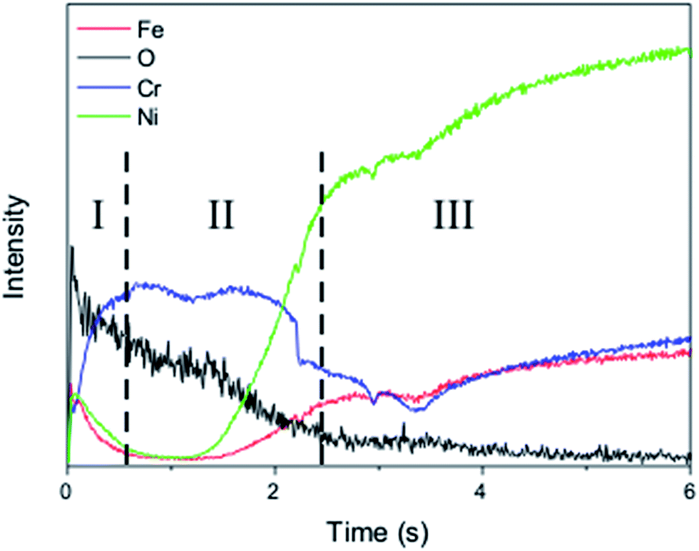 | ||
| Fig. 2 GDOES elemental depth profile for oxidized Inconel. | ||
The combination of XRD data, EDS elemental mapping and GDOES (Fig. S4, ESI†) depth profile analysis allows to conclude that during the oxidation pretreatment Fe is preferentially segregated to the outer layer (region I) forming Fe2O3 while Cr remains in the adjacent subsurface region II. Ni associates to Fe diffusion to the surface. Even though Inconel is an alloy where a chromium oxide (Cr2O3) passivation barrier is formed upon air exposure at elevated temperatures (e.g. 850 °C),5 the XRD pattern does not show the presence of this oxide on the outer layer. In fact, a continuous Cr2O3 layer is formed underneath of the other oxides, uplifting them to the outer region. These observations are in agreement with recent oxidation studies on Inconel® 600 that showed that inward oxygen diffusion promoted the formation of a Cr2O3 inner type layer, whereas Ni ions move outward.11 Earlier studies highlighted the importance of the relative rates of diffusion of elements from the bulk alloy to explain the formation of different oxide layers, in opposition to free-energy considerations (that would favor oxidation in the order Cr > Fe > Ni) and availability of metal (that would promote the oxidation order Ni > Cr > Fe).12
3.2. Growth of VACNTs on Inconel substrate
It is well-known that the VACNTs growth depends on the formation of nano-sized metal catalyst particles on the substrate surface.7,13 Hence, the granular morphology produced after heat treatment (Fig. 1a) together with its iron oxide chemical nature (Fig. S1,†1c and 2), appears as an ideal combination for the in situ direct growth on Inconel provided a reduction treatment is undertaken. This was the reason for the shorter annealing step (1 min) in a reductive mixture flow of H2 and Ar that resulted in the surface morphology presented in Fig. 3. Longer annealing times lead to the agglomeration of the small nano-sized particles into larger ones, decreasing their catalyst activity and eventually suppress the CNTs growth. As a result, an even distribution of nano-sized particles with pseudo-spherical morphology is obtained, demonstrating that the grains were restructured to a smaller size constituting ideal catalytic active sites for the CNTs growth. In fact, they promote the adsorption and dissociation of the carbon source (i.e., C2H2) on their surfaces, and the dissolution and further precipitation of the carbon atoms, leading to the growth of a CNT.13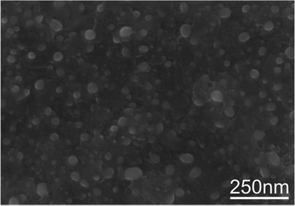 | ||
| Fig. 3 SEM image of the Inconel surface before the CNT growth step. | ||
The high number of nucleation sites leads to a high density of CNTs grown over the substrate, as shown in Fig. 4a and b. The vertical alignment with respect to the substrate is depicted from images in Fig. 4c and d. This alignment results from the sufficient density of growing CNTs that causes surface crowding constraining a preferentially unidirectional growth. This means that, as CNTs begin to grow form the densely distributed nano-sized catalyst particles, it is generally accepted that van der Waals forces among CNT neighbors cause them to all grow vertically to the substrate.14 The final height of the VACNTs after 15 min of growth was observed to be around 18 μm by 3D optical profilometry measurement, denoting a higher growth rate than that attained by hot filament CVD, where 10 μm in height forests were grown for 1 hour.9
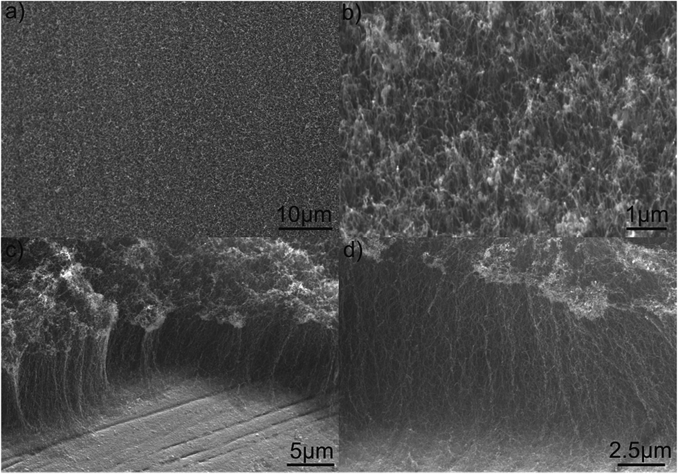 | ||
| Fig. 4 SEM images of the CNTs distribution over the substrate at different magnifications: (a) top view; (b) 45° tilted; (c and d) side views of the VACNTs. | ||
The TEM image reported in Fig. 5a depicts an overview of the CNTs taken at low magnification. The image reveals that the nanotubes are multiwalled CNTs with 14–18 nm in outer diameter. The crystallinity of the CNTs was examined by HRTEM together with SAED shown in Fig. 5b and c, respectively. The characteristic 0.34 nm inter-wall spacing of the CNTs is given in Fig. 5b and the ring-like pattern in SAED in Fig. 5c shows the (002) and (004) rings planes of the graphitic walls.
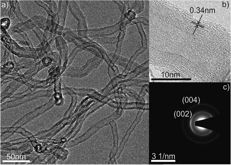 | ||
| Fig. 5 Overview TEM and HRTEM image (a and b) and SAED ring-like pattern (c) of the CNTs. | ||
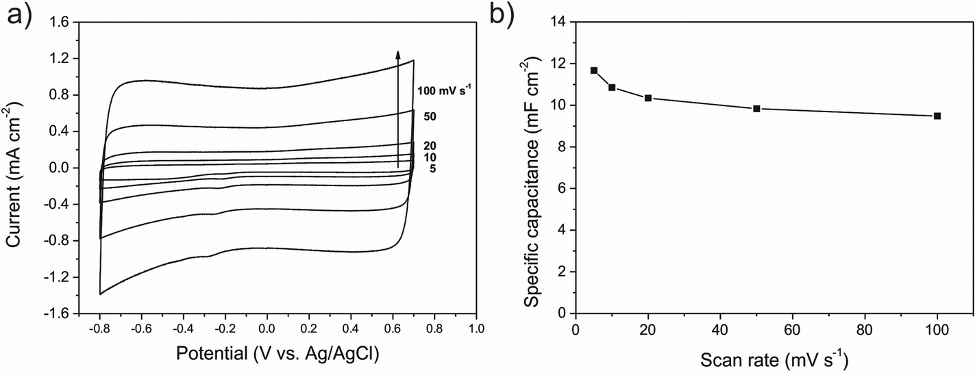 | ||
| Fig. 6 Cyclic voltammograms (a) of CNTs/Inconel electrode measured at different scan rates ranging from 5 to 100 mV s−1 and dependence of the specific capacitance derived from the CV measurements (b). | ||
Raman spectroscopy was employed to investigate the purity and the degree of graphitization of the grown VACNTs. As shown in Fig. S5 (ESI†), the Raman spectra exhibit two main bands around 1340 cm−1 (D band) and around 1575 cm−1 (G band) characteristics of multi-walled CNTs.15–18 For comparison, the CNTs were also grown on Si buffered substrate, i.e., iron thin film was deposited onto Al2O3/SiO2/Si substrate by physical vapour deposition. The strong G band corresponds to the stretching mode of the C–C bond in the graphitic plane and demonstrates the presence of crystalline graphitic carbon. On the other hand, the D band is indicative of defects in CNTs, i.e., carbonaceous impurities with sp3 bonding and broken sp2 side walls. The intensity ratio ID/IG is indicative of the degree of purity of the CNT samples.17 The lower value of this ratio indicates less defects and amorphous carbon and thus higher level of purity. The ID/IG ratio estimated from the Raman studies are ID/IG = 1.00 and 0.91 for the VACNTs grown onto Inconel substrate and Si buffered substrate, respectively. These results reveal a similar defects level of both of the VACNTs samples.
It is generally accepted that the CNT growth mechanism is dependent on the surface chemistry interactions between the carbon precursor and the existent metallic phases, and also on the presence of an underneath diffusion barrier.6,9 As above reported, Fe preferably diffuses into the surface leading to the formation of Fe2O3 that is subsequently reduced to Fe in the annealing step. As matter of fact, Fe2O3 nanoparticles have been intentionally used as pre-catalyst for VACNTs growth.19,20 For example, we already showed that a microwave-assisted synthesis of a solution of Fe(acac)3 in benzyl alcohol permitted the deposition of Fe2O3 nanoparticles onto a variety of substrates, which were shown to be the active catalysts, after the in situ reduction to metallic Fe, for the VACNTs growth.21
The Inconel surface was characterized by grazing angle XRD after the CNT growth (Fig. S6, ESI†) and the removal of the VACNTs. The pattern, on top of the reflections of Ni, shows low intensity Fe reflections and no Fe2O3. This demonstrates that, on the one hand Fe2O3 has been reduced to metallic Fe, which was the active catalyst in the CNTs growth. On the other hand, the low intensity of the Fe reflections suggests that most of the surface iron catalysts particles are lifted up during the growth, as also in agreement with the TEM image reported in Fig. S7.† The presence of these particles inside of the tubes can be due to the growth process that employs the whole Inconel surface as catalyst. Chen et al.22 suggested that stretching force causes the nano-sized catalytic particles, that are in a liquid state at the growth temperature, to elongate and finally to break into two parts, one staying at the base, while another being lifted up. It can be concluded that the CNTs grown on the Inconel follow the base growth mechanism.
No less important is the Cr2O3 layer formation underneath the outer Fe2O3 layer (Fig. 1 and 2) that acts as a diffusion barrier and supporting layer for the formation of evenly distributed nano-sized catalyst particles.9 Indeed, a Cr2O3 oxide layer has been used by others for the stabilization of Fe on Inconel and subsequent CNT growth by vapor-phase catalyst delivery CVD method.1,4–6
3.3. Electrochemical characterization
In order to prove that the VACNTs directly grown on the metallic current collector (Inconel substrate) display good electrical properties and can be used as electrode in a variety of applications electrochemical measurements have been carried out. Fig. 6a shows cyclic voltammograms (CV) of the CNTs/Inconel at different scan rates ranging from 5 to 100 mV s−1 in 1 M Na2SO4, where the potential limits are restricted from −0.8 to 0.7 V in a standard three electrode cell.It can be seen that all CV curves at the different scan rates are all of a rectangular-like shape. It is well known that a large-current, rectangular-type CV and symmetry in anodic and cathodic directions are the indications of ideal capacitor behavior of the electrode materials. This suggests that the VACNTs have very rapid current response on voltage reversal, small equivalent serial resistance (ESR) and low contact resistance with the substrate. The straight rectangular sides of I–E responses also support this feature. As a matter of fact, a large resistance will distort the response, into a narrower loop with an oblique shape, especially at a high sweep rate.20 The capacitance was derived from the cyclic voltammogram curves using the eqn (1):
 | (1) |
Galvanostatic charge–discharge measurements were also applied to characterize the properties of the CNTs/Inconel electrode, where the carbon based electrode was charge-discharged under a current density of 0.5 A g−1. Fig. 7a shows a typical current charge–discharge (E–t) curve of the CNTs/Inconel electrode. On both curves, the E–t responses of the charge process reveal a mirror-like image of their corresponding discharge counter parts and no significant IR drop was observed. It can be concluded that the resistance is low and highly charge–discharge efficiency. The Csp can be estimated according to the following eqn (2):
 | (2) |
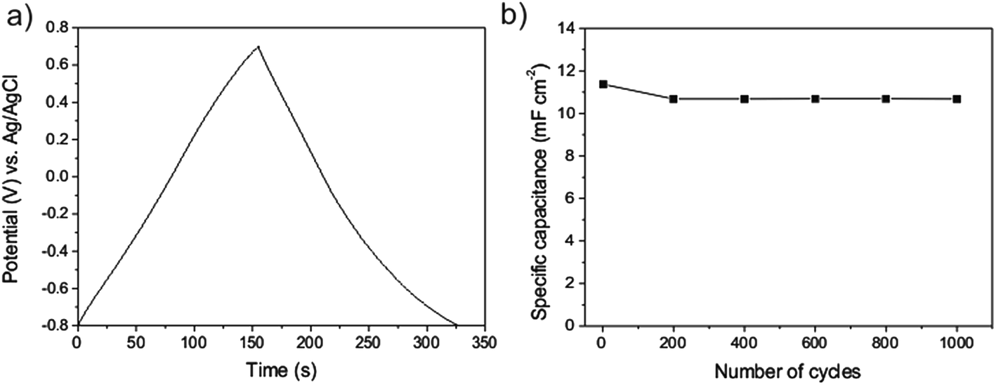 | ||
| Fig. 7 Galvanostatic charge–discharge curve (a) of the CNTs/Inconel electrode under a current density of 0.5 A g−1 and dependence of the specific capacitance on the cycle number (b). | ||
Electrochemical impedance spectroscopy results represented by Nyquist plot (Fig. S8, ESI†) consist of three frequency-dependent regions. At very high frequencies (A), the CNTs electrode behaves like a pure resistance. The equivalent series resistance (ESR) obtained from the real axis intercept of the Nyquist plot is 9.1 Ω corresponding to the sum of electrolyte resistance and contact resistance between the CNTs and the current collector (Inconel).23 At low frequency (region B), the imaginary part of the impedance sharply increases and the plot tends to a vertical line characteristic of a purely capacitive behavior. This vertical line along the imaginary axle indicates good capacitance behavior and lower ion diffusion resistance of the CNTs/electrolyte. The influence of the matt-like structure and thickness of the CNTs electrode on the access of the electrolyte to the entire available surface, can be observed in the medium frequency (C). It can be concluded that the as-prepared CNTs provide a large accessible area for the electrolyte diffusion and therefore the formation of the double layer capacitance. Moreover, these findings imply that the VACNTs exhibit low internal resistance and good dynamic charge–discharge response characteristics.
4. Conclusions
Here we have reported for the first time a simple procedure to directly grow VACNTs on an Inconel substrate by TCVD, without the addition of an external catalyst. The Inconel substrate surface acts both as catalyst and as support for the CNTs growth. The results demonstrate that the growth of VACNTs is directly related to the uniformly dispersed and densely packed nano-sized catalytic particles formed by a simple annealing of the Inconel alloy in air. This work paves the way for the growth of CNTs directly on metallic substrates which resolves the problem of adhesion of nanotubes on metallic substrates and fulfills the requirement for electrochemical applications. Further evidence in support of this statement was obtained from the cyclic voltammetry and electrochemical impedance spectroscopy. Finally, our growth process may lead to new opportunities in electrode preparation for various applications in sensors and energy storage and conversion.Acknowledgements
R. M. Silva is very grateful to FCT for the grant SFRH/BD/90844/2012. The RNME – Pole University of Aveiro, FCT Project REDE/1509/RME/2005 is acknowledged. The authors would like to acknowledge A. J. S. Fernandes and M. C. Ferro from University of Aveiro for the Raman spectra and TEM studies, respectively. This work was developed in the scope of the project CICECO-Aveiro Institute of Materials (Ref. FCT UID/CTM/50011/2013), financed by national funds through the FCT/MEC and co-financed by FEDER under the PT2020 Partnership Agreement.References
- S. Talapatra, S. Kar, S. K. Pal, R. Vajtai, L. Ci, P. Victor, M. M. Shaijumon, S. Kaur, O. Nalamasu and P. M. Ajayan, Nat. Nanotechnol., 2006, 1, 112–116 CrossRef CAS PubMed.
- L. Gao, A. Peng, Z. Y. Wang, H. Zhang, Z. Shi, Z. Gu, G. Cao and B. Ding, Solid State Commun., 2008, 146, 380–383 CrossRef CAS PubMed.
- H. Zhang, G. Cao and Y. Yang, Energy Environ. Sci., 2009, 2, 932–943 CAS.
- S. K. Pal, S. Talapatra, S. Kar, L. Ci, R. Vajtai, T. Borca-Tascicu, L. S. Schadler and P. M. Ajayan, Nanotechnology, 2008, 19, 045610–045615 CrossRef CAS PubMed.
- J. B. Bult, W. G. Sawyer, P. M. Ajayan and L. S. Schadler, Nanotechnology, 2009, 20, 085302–085309 CrossRef CAS PubMed.
- S. K. Pal, S. Kar, S. Lastella, A. Kumar, R. Vajtai, S. Talapatra, T. Borca-Tascicu and P. M. Ajayan, Carbon, 2010, 48, 844–853 CrossRef CAS PubMed.
- D. Mata, R. M. Silva, A. J. S. Fernandes, F. J. Oliveira, P. M. F. J. Costa and R. F. Silva, Carbon, 2012, 50, 3585–3606 CrossRef CAS PubMed.
- S. Sridhar, L. Ge, C. S. Tiwary, A. C. Hart, S. Ozden, K. Kalaga, S. Lei, S. V. Sridhar, R. K. Sinha, H. Harsh, K. Kordas, P. M. Ajayan and R. Vajtai, ACS Appl. Mater. Interfaces, 2014, 6, 1986–1991 CAS.
- W. Yi and Q. Yang, Diamond Relat. Mater., 2010, 19, 870–874 CrossRef CAS PubMed.
- W. Yi and Q. Yang, Appl. Phys. A, 2010, 98, 659–669 CrossRef CAS.
- J. Xiao, N. Prud’homme, N. Li and V. Ji, Appl. Surf. Sci., 2013, 284, 446–452 CrossRef CAS PubMed.
- J. M. Francis, J. A. Jutson and J. H. Buddery, J. Mater. Sci., 1967, 2, 78–87 CrossRef CAS.
- H. Ma, L. Pan and Y. Nakayama, Carbon, 2011, 49, 854–861 CrossRef CAS PubMed.
- Y. Lan, Y. Wang and Z. F. Ren, Adv. Phys., 2011, 60, 553–678 CrossRef CAS PubMed.
- F. Tuinstra and J. L. Koenig, J. Chem. Phys., 1970, 53, 1126–1130 CrossRef CAS PubMed.
- A. M. Rao, A. Jorio, M. A. Pimenta, M. S. S. Dantas, R. Satio, G. Dresselhaus and M. S. Dresselhaus, Phys. Rev. Lett., 2000, 84, 1820–1823 CrossRef CAS.
- M. S. Dresselhaus, G. Dresselhaus, R. Satio and A. Jorio, Phys. Rep., 2005, 409, 47–99 CrossRef PubMed.
- R. A. DiLeo, B. J. Landi and R. P. Raffaelle, J. Appl. Phys., 2007, 101, 064307–064312 CrossRef PubMed.
- M. Felisberto, L. Sacco, I. Mondragon, G. H. Rubiolo, R. J. Candal and S. Goynes, Mater. Lett., 2010, 64, 2188–2190 CrossRef CAS PubMed.
- K. Yamada, A. Kaneko, H. Kato and Y. Homma, Mater. Express, 2012, 2, 257–260 CrossRef CAS PubMed.
- R. M. Silva, A. Pucci, C. Marichy, D. Mata, M. C. Ferro, R. F. Silva and N. Pinna, CrystEngComm, 2012, 14, 48–52 RSC.
- X. Chen, R. Wang, J. Xu and D. Yu, Micron, 2004, 35, 455–460 CrossRef CAS PubMed.
- B. E. Conway, Electrochemical Supercapacitors: Scientific Fundamentals and Technological Applications, Plenum, New York, 1999 Search PubMed.
Footnote |
| † Electronic supplementary information (ESI) available. See DOI: 10.1039/c5ta03734d |
| This journal is © The Royal Society of Chemistry 2015 |