
 Open Access Article
 This Open Access Article is licensed under a
 Creative Commons Attribution 3.0 Unported Licence
Smooth perovskite thin films and efficient perovskite solar cells prepared by the hybrid deposition method†
Shenghao
Wang
,
Luis K.
Ono
,
Matthew R.
Leyden
,
Yuichi
Kato
,
Sonia R.
Raga
,
Michael V.
Lee
and
Yabing
Qi
*
Energy Materials and Surface Sciences Unit (EMSS), Okinawa Institute of Science and Technology Graduate University (OIST), 1919-1 Tancha, Kunigami-gun, Onna-son, Okinawa 904-0495, Japan. E-mail: Yabing.Qi@OIST.jp
First published on 28th May 2015
Abstract
We provide details on the development of instrumentation and methodology to overcome the common difficulties that the vacuum-related techniques face for fabrication of perovskite thin films and perovskite solar cells (PSCs). Our methodology relies on precisely controlling the flow of methylammonium iodide (CH3NH3I, MAI), which has a high-vapor pressure nature, and the deposition rate of metal halides (PbCl2 or PbI2). This hybrid deposition method allows the growth of perovskite films with smooth surface, good crystallinity, high surface coverage, uniform chemical composition and semi-transparency. We also systematically investigated the effects of the evaporation source materials (PbCl2![[thin space (1/6-em)]](https://www.rsc.org/images/entities/char_2009.gif) :MAI versus PbI2:MAI), substrate temperatures, and post-annealing on the properties of perovskite films, as well as device performances based on this method. By employing a thin perovskite film (<200 nm), the power conversion efficiency of PSC can be as high as 11.5%.
:MAI versus PbI2:MAI), substrate temperatures, and post-annealing on the properties of perovskite films, as well as device performances based on this method. By employing a thin perovskite film (<200 nm), the power conversion efficiency of PSC can be as high as 11.5%.
Introduction
Perovskite materials CH3NH3PbX3 [X = Cl, I or Br] have recently attracted increasing attention due to their desirable opto-electronic properties, such as strong light absorption for almost the whole visible range, long exciton diffusion lengths, long charge-carrier lifetime, and high carrier mobility.1–9 Since the first report by Miyasaka et al.,3 tremendous progress in achieving high performance perovskite solar cells (PSCs) with power conversion efficiencies (PCEs) of 12–20.1% has been made over the past 5 years,10–17 showing that PSCs have the potential to compete with the well-established silicon photovoltaic industry in the near future.Perovskite thin films can be prepared by a range of deposition techniques, such as spin-coating,11,18–20 co-evaporation,14,15,21,22 vapor assisted solution process (VASP),23 hybrid chemical vapor deposition (HCVD),24 vacuum sequential deposition,25,26 and spray-deposition.27 Generally, mesoporous metal oxides (e.g., TiO2 and Al2O3) are used to obtain high PCEs for solution-based methods, in which perovskite is scaffolded by the mesoporous matrices.18,28–32 However, it requires a high-temperature sintering process, limiting the application on flexible substrates.15 Although the planar-type device architecture is particularly attractive due to its simple cell configuration and possible fabrication using a solution process, depositing a homogeneous perovskite film with a thickness comparable to the charge diffusion length has been proven to be difficult.14,33
On the other hand, vacuum evaporation methods offer some unique advantages. (1) Vacuum evaporation methods are desirable to achieve high-purity films, because the films are formed in a vacuum chamber by sublimation of powder materials after extensive outgassing. (2) The initial nominal stoichiometry of methylammonium iodide (CH3NH3I, MAI) and lead halides can be well controlled in both solution and vacuum evaporation methods. However, in solution methods the solubility of reactants in solvents is an additional parameter that needs be considered. For example, it is difficult to dissolve PbCl2 in N,N-dimethylformamide when the MAI:PbCl2 molar ratio is lower than 3:1.32 In this sense vacuum evaporation methods are advantageous because the ratio of the two reactants (i.e. lead halide and MAI) can be tuned and therefore it is not limited by solubility. (3) It is suitable to prepare multi-layered structures of thin films to fine tune the charge collection/injection properties at interfaces among multilayers34,35 or precisely control the electrical properties by doping, a well-established technique in organic solar cells and organic light-emitting diodes.36,37 (4) Perovskite films can be deposited by a vacuum evaporation method on a variety of substrates without concerning solvent compatibilities allowing different device architectures with various contact buffer layers: TiO2,14 NiO/CuSCN,22 poly(3,4-ethyene dioxythiophene):(polystyrene sulfonic acid) (PEDOT:PSS),21 and poly(N,N′-bis(4-butylphenyl)-N,N′-bis(phenyl)benzidine) (poly-TPD).15,21 (5) In addition, vacuum evaporation methods are compatible with conventional processing methods that have been well established for silicon, cadmium telluride (CdTe) and copper indium gallium (di)selenide (CIGS) solar cells. Hybrid tandem junction solar cells obtained by combining PSCs with these first- or second-generation solar cells are very promising to obtain solar cells with even higher efficiencies.
Despite the aforementioned advantages, to date only a handful of studies have utilized vacuum-based deposition to fabricate perovskite layers and solar cells, in sharp contrast to a myriad of solution-based methods and their variants.38–41 Liu et al.14 and Subbiah et al.22 reported uniform deposition of perovskite layers by co-evaporating PbCl2:MAI. Similarly, Malinkiewicz et al. fabricated PSCs with a PCE as high as 14.8% by using PbI2 and MAI as evaporation materials.15,21 However, difficulties in calibrating the quartz crystal thickness monitor parameters for MAI were mentioned in all these studies as a key challenge to achieve reproducible and controlled film preparation. The evaporation rate of MAI is difficult to be calibrated and controlled because of its relatively high vapor pressure. To solve such a challenge, our group recently developed a new methodology (the hybrid deposition method) to monitor the deposition rate of MAI by orientating the thickness monitor opposite to the evaporation direction of MAI to avoid the cross-talk from the metal halide source.42 Also, a two-step sequential deposition method was recently reported for the fabrication of PSCs.25,26 In this method, a metal halide layer was first deposited on the substrate, and then the MAI layer was subsequently deposited. However, the MAI diffusion depth is limited leaving the bottom metal halide layer unreacted.25 Additionally, similar difficulties faced in the co-evaporation method are also encountered in the sequential deposition method.
In this work, we first present the key challenges of the vacuum-based deposition methods and show how our hybrid deposition method can be used to alleviate these issues. Then we systematically study the effects of evaporation source materials (PbCl2:MAI versus PbI2:MAI), substrate temperatures, and post-annealing on the perovskite film quality (i.e. coverage, uniformity, and crystallinity), as well as device performance. Using optimized conditions, we were able to reliably deposit perovskite films with very smooth surface, good crystallinity, high surface coverage, uniform chemical composition and semi-transparency. PSCs with high performance can be achieved at room temperature. Such a comprehensive study is expected to not only provide a full guide of convenient and reliable fabrication of PSCs by the hybrid deposition method, but also provide insight into the development of a low cost building integrated photovoltaic (BIPV) window.
Experimental section
Instrumentation and methodology: hybrid deposition
In a typical co-evaporation system, the precise control of the deposition rates is important for obtaining a uniform chemical composition across the film thickness. Generally, a quartz crystal thickness monitor (so-called “sensor” hereafter) is used to measure the deposition rate of the material. It is generally necessary to perform the thickness calibration, i.e. to use another technique (e.g., atomic force microscopy (AFM) or profilometry) to determine the film thickness and find out its relationship with the nominal thickness measured by the sensor. However, in the case of MAI, the calibration procedure is difficult due to the formation of a non-uniform layer dominated by the Volmer-Weber or Stranski-Krastanov growth mode. The morphology of the MAI layer deposited on a Si substrate is shown in Fig. S1(a) (ESI).† In addition, MAI has a relatively high vapor pressure and is found to be able to deposit everywhere in the chamber. For instance, the MAI layer was observed (confirmed by XRD and AFM, not shown here) on the top surface of a substrate that is facing the opposite direction of the MAI source. In comparison, metal halides deposit mainly along the line-of-sight direction from the source. The high vapor pressure of MAI also leads to cross-talking to the reading of the sensor used to monitor the evaporation rate of metal halides.Considering the challenges to control the individual deposition rates as mentioned above, we developed the hybrid deposition method to precisely control the deposition rates of both materials and the film thickness to obtain a high quality perovskite film. Fig. 1 shows the schematic illustration of the deposition setup. Metal halides (PbCl2 or PbI2) and MAI were used as evaporation source materials. Substrates are placed on a sample holder at a distance of ∼25 cm above the metal halide source. To achieve a high level of film thickness and composition uniformity, two widely open dish-like crucibles are used for evaporating the two source materials. A shield is fixed between the two sources, in order to minimize the thermal “cross-talking” between them, and in particular, to reduce the influence of the metal halide source heating on the MAI source. Such a consideration is often necessary when evaporating two materials with distinctively different evaporation temperatures, e.g., PbI2 typically evaporates at ∼250 °C while MAI evaporates at only ∼70 °C. A shutter with a diameter larger than that of the source crucible is used. It should be emphasised that this shutter is always closed during the evaporation of MAI. The shutter blocks the direct deposition of MAI and avoids the high flux of MAI hitting directly the substrate area, which may cause the non-uniform composition in the film.
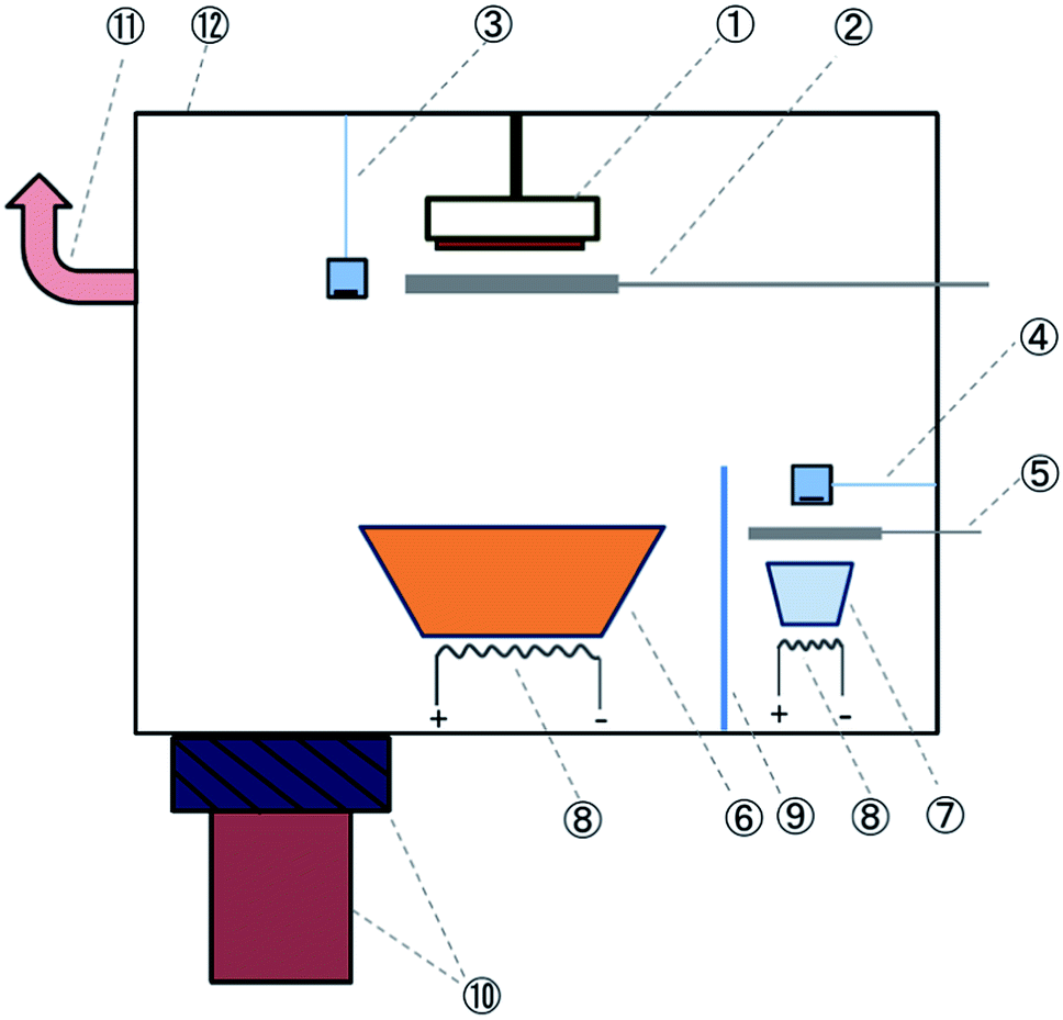 | ||
| Fig. 1 Schematic illustration of the hybrid deposition method using metal halides and MAI as source materials. Part numbers are defined as follows: (1) substrate holder stage that allows cooling and heating; (2) substrate shutter; (3) thickness monitor (sensor 1) for monitoring the deposition rate of metal halides; (4) thickness monitor (sensor 2) for monitoring the nominal deposition rate of MAI; (5) MAI source shutter, which is always closed during perovskite film growth; (6) widely open dish-shaped crucible for the evaporation of metal halides; (7) crucible for MAI vapor deposition; (8) filaments for heating the source materials; (9) shield for separating the two sources to avoid the thermal cross-talking; (10) pumping system comprising a gate-valve and a turbo molecular pump; (11) additional pump line to guide the MAI flow with respect to the substrate position; (12) main vacuum chamber. | ||
There are two sensors in the chamber. The density, z-factor and tooling factor parameters of sensor 1 are set to be 5.85 g cm−3, 0.8 and 7, respectively. For sensor 2, they are nominally set to be 0.2 g cm−3, 0.2, and 3. These optimized parameters enhance the sensitivity of sensor 2 for the rate detection of MAI. The effect of MAI evaporation on sensor 1 is expected to be minimal because MAI has a much smaller density than metal halides. Therefore sensor 1 mainly monitors the rate of metal halides. Sensor 2 is located at the MAI source side and its height is below the height of the shield that separates the two sources. Therefore, it only detects the nominal deposition rate of MAI without the influence of the metal halide source. Further details on the optimization procedure for sensor 2 can be found in the ESI.†
In the hybrid deposition method, after the substrates (multiple substrates can be mounted depending on the substrate size) are transferred into the chamber (base pressure < 4.0 × 10⁻⁶ Torr), the metal halide source is heated and the rate is monitored by sensor 1. After reaching a certain rate on sensor 1, we start to heat MAI. As MAI vapor is produced, the pressure inside the chamber increases substantially to ∼10−3 Torr. The evaporation of MAI relies primarily on controlling the vapor and flow of MAI inside the chamber. By optimizing the MAI vapor pressure and flow, a precise control of the deposition rate for MAI can be achieved. The control of pressure is crucial, because if the pressure is too high, it will eventually affect the vapor flow condition and influence the rate of metal halides. To avoid this detrimental effect, a gate valve is used to maintain the pressure constant at a value of ∼3 × 10⁻³ Torr. The gate valve also allows the control of the MAI vapor pressure inside the chamber (i.e., setting the gate valve to a pre-determined opening position) without being pumped out, resulting in a more efficient use of MAI. An additional pumping line (HiCube80, Pfeiffer) is connected at the top part of the chamber (at the same height as the samples), which provides better vapor flow uniformity across the substrate surface. The uniform vapor flow makes the sensor 2 reading stable and is key to achieve reproducible film deposition. Typical readings of PbI2 and MAI from sensors 1 and 2 are shown in Fig. S2 ESI.† When metal halides and MAI meet on the substrate, the reaction occurs to form perovskite. When the desired thickness is achieved, the heating of the two sources is stopped and the gate valve is immediately opened to quickly pump out the remaining vapor of excess MAI to avoid the formation of a MAI rich layer on the sample surface. Then the samples are transferred to a home-designed nitrogen suit-case immediately after the completion of evaporation that avoids air exposure induced contamination or degradation of perovskite films.
MAI synthesis
MAI was synthesized according to a literature procedure.32 Briefly, hydroiodic acid solution was gradually added to methyl amine ethanol solution that was kept stirring in an ice-bath. Ethanol and water from the mixed solution were evaporated using a rotary evaporator (BUCHI, Rotavapor R-3). The precipitated yellow-colored crystals were dissolved in hot ethanol, and cooled in a refrigerator at 5 °C for recrystallization. Subsequently, the crystals were filtered and washed with tetrahydrofuran and diethyl ether resulting in a white crystal powder. We dried and kept the MAI in a N2 glove box (H2O < 0.1 ppm and O2 < 0.1 ppm).Perovskite film preparation and characterization
Perovskite films were prepared by the hybrid deposition method by using either PbCl2:MAI or PbI2:MAI. In the case of PbCl2:MAI, the evaporation rate ratios for PbCl2:MAI were varied from 0.76, 0.61, 0.52, 0.39, 0.30, and 0.21, corresponding to films 1, 2, 3, 4, 5 and 6, respectively. In the case of PbI2:MAI, the evaporation rate ratios for PbI2:MAI were varied from 2.27, 1.82, 1.55, 1.18, and 0.82, corresponding to films 7, 8, 9, 10 and 11, respectively. The film thicknesses were measured by using a profilometer (Dektak XT, Bruker). The crystal structure of films was characterized by X-ray diffraction (XRD, D8 Discover, Bruker). High-resolution X-ray photoelectron spectroscopy (HRXPS, Axis Ultra, KRATOS) measurements were performed to obtain the surface chemical composition of the films. The chemical composition of the bulk film was studied by X-ray fluorescence (XRF, XGT-7200, Horiba). The elemental sensitivity of the instrument was calibrated by using a PbI2 film as the reference. The morphological properties were investigated by atomic force microscopy (AFM, MFP-3D series, Asylum Research). The transmittance was measured using a UV/Vis spectrometer (JUSCO Inc., V-670).
Substrate temperature dependence and post-annealing process
For the substrate temperature dependence experiment, the substrate temperatures were varied from −50 to 110 °C. The low temperature was achieved by cooling down the sample holder using liquid nitrogen. High temperatures (>20 °C) were attained by four thermal resistive elements that are installed inside the sample holder. The fluctuation in temperature is ±2 °C. The post-annealing process of the as-deposited films was carried out on a hot plate at different temperatures (100–140 °C) and different annealing times in a N2-filled glove box. During the sample transfer from the deposition chamber to the N2-filled glove box, an additional home-designed N2-filled suit-case was used to avoid air exposure.Device fabrication and performance characterization
Patterned fluorine-doped tin oxide (FTO) glasses (Pilkington, 7 Ω □−1) were used as substrates. The device structure is FTO/TiO2/perovskite/spiro-MeOTAD/Au. A compact layer of TiO2 (thickness ∼ 70 nm) is used as an electron transport layer (ETL), which was prepared via spray pyrolysis using a precursor solution of acetylacetone, Ti(IV) isopropoxide and anhydrous ethanol (3:3:2) on a pre-heated hot plate at 480 °C. The absorber layer of CH3NH3PbI3 perovskite was deposited by the hybrid deposition method. After the deposition of the perovskite layer, the samples were in situ transferred to the home-designed N2-filled suit-case and then to the N2 glove box. Subsequently, a hole transport layer (HTL) was spin-coated at 4000 rpm for 60 s by mixing three compounds: spiro-MeOTAD (2,2′,7,7′-tetrakis(N,N-di-p-methoxy-phenylamine)-9,9′-spirobifluorene (Merck) (72.5 mg), 17.5 μL of Li-bis(trifluoromethanesulfonyl)-imide (LiTFSI, Sigma) dissolved in acetonitrile (52 mg/100 μL), and 28.8 μL of tert-butylpyridine (t-BP, Sigma) dissolved in 1 mL chlorobenzene. Finally, the Au top electrode (100 nm) was deposited by thermal evaporation. The cell active area was 6 mm2, as determined by the overlapping area of the FTO cathode and Au anode with a shadow mask. The current density versus voltage (J–V) characteristics of the devices were measured with a J–V source meter (Keithley 2420) under AM 1.5 G 100 mW cm−2 simulated solar light. The photovoltaic parameters were obtained at 0.17 V s−1 scan rate and setting the voltage sweep starting from positive to the negative voltage during J–V measurements.
Results and discussion
Perovskite formation from PbCl2![[thin space (1/6-em)]](https://www.rsc.org/images/entities/h3_char_2009.gif) :MAI
:MAI
It has been demonstrated that high PCEs (15.4% (ref. 14) and 14.8% (ref. 25)) can be obtained by either co-evaporating PbCl2:MAI or co-evaporating PbI2:MAI. In the case of PbCl2, the chemical formula “CH3NH3PbI3−xClx” is generally used to represent the mixed methylammonium lead halide perovskite.14,22 However, the incorporation of Cl and its role are still under debate.43,44 In the case of PbI2, the chemical formula is “CH3NH3PbI3” for perovskite.14,21 To understand how metal halides react with MAI and how the perovskite film formation takes place, it is essential to systematically study these two cases by using different metal halides, namely, PbCl2 or PbI2.
For the co-evaporation method, it is important to precisely control the composition of films by choosing suitable evaporation rates for the two source materials. In the co-evaporation system described by Liu et al., the optimized molar ratio of PbCl2:MAI = 1:4 was used.14 On the other hand, Subbiah et al. reported the optimized molar ratio of PbCl2:MAI to be 1:5.4,22 substantially different from Liu et al.'s report. This suggests that the optimal rates and ratio between the two source materials are highly dependent on the deposition system, which is another indication of unusual evaporation properties of MAI. To understand the perovskite film formation and to further control the film growth, it is necessary to investigate the properties of the films prepared at different evaporation rate ratios of PbCl2:MAI.
First of all, it is necessary to characterize the properties of the pure PbCl2 layer and MAI film, such as XRD features and morphologies. In addition, PbI2 sometimes exists in the perovskite film even though the precursors are PbCl2 and MAI.16 The morphology properties and XRD spectra of PbCl2, PbI2 and MAI films deposited by the hybrid deposition method are shown in Fig. S1 and S3 ESI.†Fig. 2(a) shows the XRD spectra of the films prepared by the hybrid deposition method using different evaporation rate ratios between PbCl2 and MAI. Films 1 to 6 correspond to the samples using the decreasing evaporation rate ratio of PbCl2:MAI from 0.76 to 0.21. XRD features differ as the evaporation rate ratio varies. When the ratio is 0.76 (film 1), three main diffraction peaks at 15.6°, 31.5° and 48.0° are found, corresponding to the CH3NH3PbCl3 phase.14,16 Phase purity is inferred from the XRD spectrum, because no peaks associated with remaining PbCl2 and other phases of perovskite such as CH3NH3PbI3 are observed. The decrease in the PbCl2:MAI ratios (0.61 for film 2 and 0.52 for film 3) induces a mixture of CH3NH3PbCl3 and CH3NH3PbI3 phases, as well as PbI2 indicated by the diffraction peak at 12.6°. When the PbCl2:MAI ratio is further decreased to 0.39 (film 4), the XRD spectrum only shows 14.0°, 28.3°, and 43.0° diffraction peaks, corresponding to the (110), (220) and (330) planes of the halide perovskite CH3NH3PbI3 film with an orthorhombic crystal structure.14 If the ratio of PbCl2:MAI decreases to 0.30 (film 5), except for the main diffraction peaks of CH3NH3PbI3, a new diffraction peak at 11.4° appears in the XRD patterns. This peak is likely associated with a H2O-incorporated perovskite complex formed during the ex situ XRD measurements due to the excess MAI in the perovskite film.45–47 In addition, the intensity of the perovskite peaks of film 5 becomes lower than that of film 4. With further decrease of the ratio of PbCl2:MAI to 0.21 (film 6), the perovskite peaks completely disappear and three distinct peaks at 9.7°, 19.6° and 29.6° dominate the XRD pattern, which corresponds to the formation of a MAI rich film. The diversity of the presented XRD spectra suggests not only the importance of precise control of the ratio between PbCl2 and MAI, but also provides vital information regarding the reaction, which will be discussed in the next section.
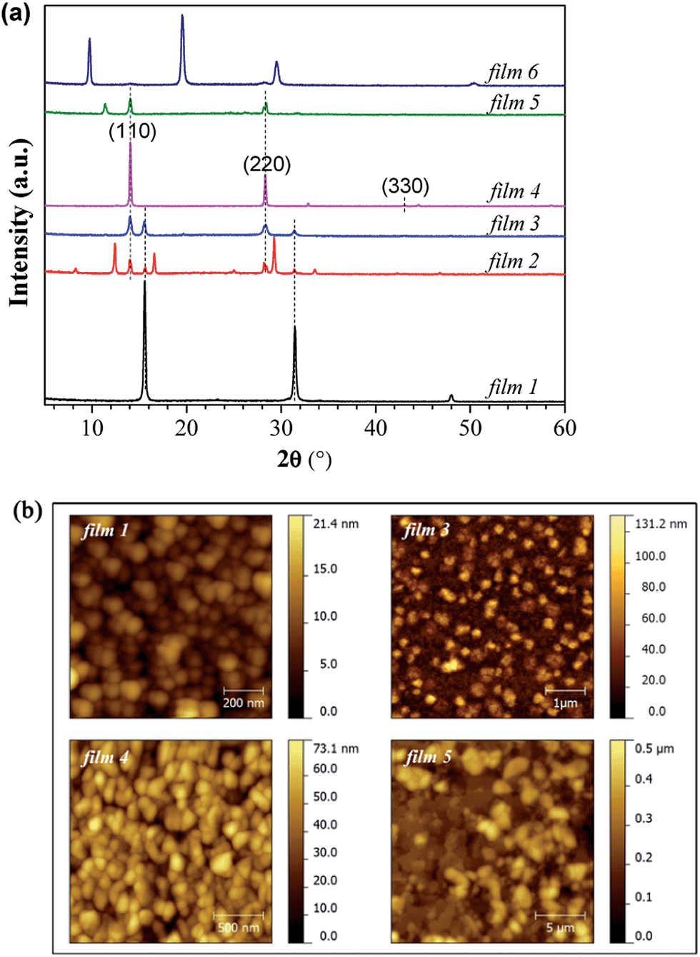 | ||
| Fig. 2 (a) XRD spectra and (b) AFM topography images of the films prepared by the hybrid deposition method using different evaporation rate ratios between PbCl2 and MAI. Vertical dashed lines are intended as guides to the eye. Si (100) with native oxide was used as a substrate. Films 1 to 6 correspond to the samples in the order of decreasing evaporation rate ratios of PbCl2:MAI from 0.76 to 0.21. The RMS roughness values are 2.9, 17.6, 11.3 and 76.7 nm for films 1, 3, 4 and 5, respectively. | ||
The morphological properties of the films with different phases, namely films 1, 3, 4 and 5, were characterized by AFM measurements, as shown in Fig. 2(b). Root mean square (RMS) is used to quantify surface roughness. The films 1, 3 and 4 show uniform and full coverage on the substrates, while film 5 is not uniform. The pure CH3NH3PbCl3 film (film 1) has a very smooth surface (RMS = 2.9 nm) with a grain size of ∼50 nm. When the film consists of a mixture of CH3NH3PbCl3 and CH3NH3PbI3 (film 3), two distinct features with both small and big grains are observed from the AFM image, which may represent the chloride and iodide perovskites, respectively. The pure CH3NH3PbI3 film (film 4, RMS = 11.3 nm) has a much bigger grain size of ∼100 nm. When the excess MAI is contained in the film (film 5), the film shows a substantially rougher surface (RMS = 76.7 nm).
High resolution X-ray photoelectron spectroscopy (XPS) and X-ray fluorescence (XRF) measurements were carried out to determine the chemical composition of the perovskite films. Fig. 3 shows the XPS spectra of the top surface of films 3, 4 and 6. The Cl 2p peak is observed only in film 3 (Fig. 3(a)), which is assigned to the CH3NH3PbCl3 phase. In the case of the absence of CH3NH3PbCl3 for film 4, there is no Cl peak. The XRF results show that the atomic ratio of I/Pb in the bulk of film 4 is around 3.01 (see Fig. S4 of ESI†), suggesting that this perovskite film has well matched stoichiometry. This is also consistent with the pure CH3NH3PbI3 phase as revealed from the XRD result as discussed above. Although XPS is a surface-sensitive technique providing chemical elemental information with a probing depth of a few nanometers, we suppose that a negligible amount of Cl is incorporated into the bulk film. This result is consistent with the report by Yu et al., in which XPS depth profile measurement by sputtering the perovskite films (prepared by the solution method, around 310 nm thick) with an Ar ion gun was performed to investigate the chemical composition from the surface to bulk.43 No signal related to the Cl 2p photoelectrons was found in the bulk perovskite film and only 1% Cl could be detected at the bottom 20 nm of the film.43 Therefore, the chemical formula of “CH3NH3PbI3” is more precise than “CH3NH3PbIxCl3−x” to represent the perovskite in this work. The peak positions of I 3d, Pb 4f, C 1s and N 1s core levels (Fig. 3(b)–(e)) for films 3 and 4 are nearly the same, because the chemical environments for these elements are similar for CH3NH3PbCl3 and CH3NH3PbI3. The C 1s core levels show two distinct peaks, which are assigned to C–N and C–C bonds, respectively.48 For film 6, both C 1s and I 3d core levels shift to higher binding energies, which is attributed to the charging effect by the rich MAI film. Thus, the XPS results presented here corroborate the XRD results. In addition, a minimal oxygen level (Fig. 3(f)) is present in the XPS measurements, confirming the cleanness of the sample.
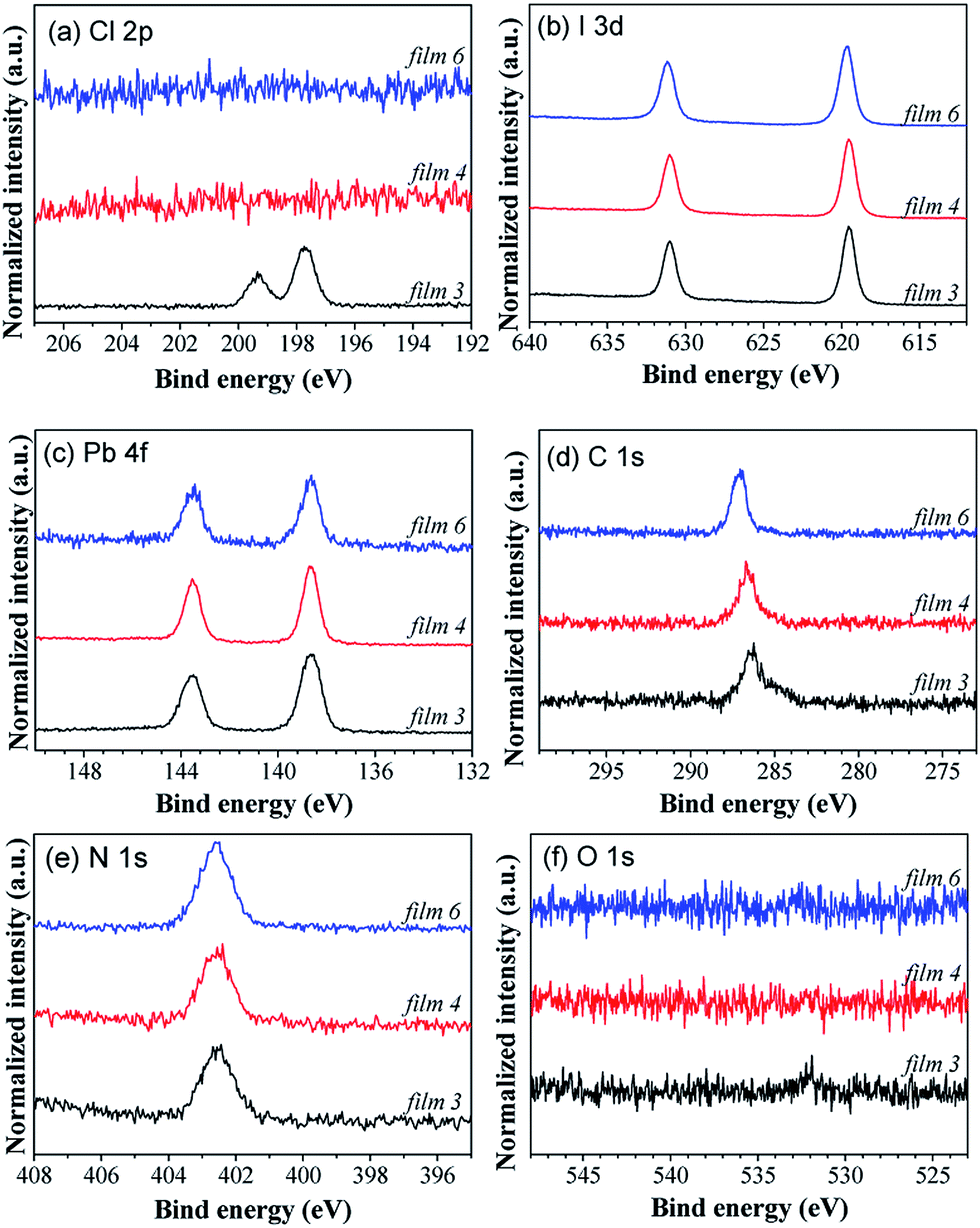 | ||
| Fig. 3 XPS core level spectra of (a) Cl 2p, (b) I 3d, (c) Pb 4f, (d) C 1s, (e) N 1s and (f) O 1s of the top surface of perovskite films deposited by the hybrid deposition method. Films 3, 4 and 6 correspond to perovskite films with the mixture of CH3NH3PbCl3 and CH3NH3PbI3, the CH3NH3PbI3, and the rich MAI, respectively. | ||
To investigate the influences of the compositions of the perovskite films on the device performances, PSCs were fabricated employing films 1 and 4. The device structure is FTO/TiO2 (70 nm)/perovskite (50 nm)/spiro-MeOTAD (100 nm)/Au (100 nm), as illustrated in Fig. 4(a). Fig. 4(b) shows the J–V curves of the devices with different compositions in perovskite films. The device with film 1 exhibits very poor photovoltaic properties because of the large bandgap (3.1 eV) of CH3NH3PbCl3,49 which is almost colorless and a poor light absorber. The device employing film 4 shows a reasonable PCE with an open-circuit voltage (Voc) of 1.029 V, a short-circuit current (Jsc) of 13.14 mA cm−2, a fill factor (FF) of 42.67%, and an overall PCE of 5.77% under 1 sun illumination. This is because the absorber layer of film 4 is pure CH3NH3PbI3 perovskite, which has strong light absorption and good charge-transport properties for photo-generated free carriers. We observed that the devices show hysteresis (see Fig. S5 of ESI†), which is commonly observed in planar structured perovskite solar cells.
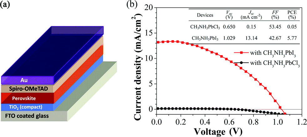 | ||
| Fig. 4 (a) Schematic illustration of the PSC device structure consisting of FTO/TiO2/perovskite/spiro-MeOTAD/Au. (b) J–V curves of the devices with CH3NH3PbCl3 and CH3NH3PbI3 perovskite films under 1 sun illumination. The table as the inset in (b) shows the photovoltaic parameters of the devices. | ||
Perovskite formation from PbI2:MAI
In this section, the influence of metal halides by changing PbCl2 to PbI2 is investigated on the perovskite film formation. Fig. 5(a) shows the XRD spectra of the films prepared by the hybrid deposition method using different evaporation rate ratios between PbI2 and MAI. Films 7 to 11 correspond to the samples by systematically decreasing the evaporation rate ratios of PbI2:MAI from 2.27 to 0.82. When the PbI2:MAI ratio is as large as 2.27 (film 7), the film shows a characteristic diffraction peak at 12.6°, which corresponds to the (001) plane of PbI2. This suggests that excess PbI2 is present in the film. The diffraction peaks at 14.1°, 20.0°, 23.4°, 24.0°, 28.4°, 31.8°, 40.5°, and 43.1°, correspond to the (110), (200), (211), (202), (220), (310), (224) and (330) planes of CH3NH3PbI3 perovskite, respectively. When the ratio of PbI2:MAI decreases to 1.82 (film 8), the intensity of the PbI2 diffraction peak decreases, suggesting that the un-reacted PbI2 becomes less than that in film 7. As the ratio of PbI2:MAI equals to 1.55 (film 9), no PbI2 peak is observed and only pure CH3NH3PbI3 perovskite film forms. As the ratio of PbI2:MAI further decreases (1.18 for film 10 and 0.82 for film 11), the intensity of perovskite peaks decreases and the diffraction peak at 11.4° is observed, which indicates the presence of excess MAI.
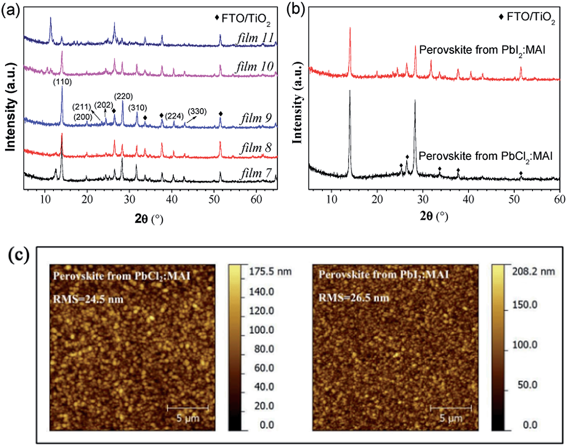 | ||
| Fig. 5 (a) XRD spectra of perovskite films prepared by the hybrid deposition method using different evaporation rate ratios between PbI2 and MAI. Films 7 to 11 correspond to the samples in the order of decreasing the evaporation rate ratios of PbI2:MAI from 2.27 to 0.82. (b) XRD spectra and (c) AFM topography images of perovskite films prepared from PbCl2:MAI and PbI2:MAI under optimized conditions. The RMS roughness values in (c) are 24.5 and 26.5 nm for PbCl2:MAI case and PbI2:MAI case, respectively. The substrates for all samples are TiO2/FTO coated glass. | ||
Interestingly, the XRD features of the perovskite films are different in the cases of PbCl2 and PbI2. The number of diffraction peaks of perovskite films formed from PbI2:MAI is much larger than that from PbCl2:MAI. Fig. 5(b) shows the XRD spectra of perovskite films prepared from PbCl2:MAI and PbI2:MAI under optimized conditions. The perovskite film prepared from PbCl2:MAI is more oriented than that from PbI2:MAI. Based on the discussion of the XRD patterns, the following reaction steps are proposed to take place for the perovskite film formation.18
| PbCl2 + 2CH3NH3I → 2CH3NH3Cl + PbI2 | (1) |
| PbCl2 + CH3NH3Cl → CH3NH3PbCl3 | (2) |
| PbCl2 + 3CH3NH3I → CH3NH3PbI3 + 2CH3NH3Cl | (3) |
| PbI2 + CH3NH3I → CH3NH3PbI3 | (4) |
In the PbCl2 case, when excess PbCl2 is present, reactions (1) and (2) occur, forming a pure CH3NH3PbCl3 film. As the ratio of PbCl2:MAI reduces, the formed film consists of CH3NH3PbCl3 and CH3NH3PbI3 and/or PbI2via reactions (1), (2) and (4). This suggests that MACl is generated when MAI is insufficient, because the reaction (1) must occur to form a pure CH3NH3PbCl3 phase. When the PbCl2:MAI ratio is further decreased to reach the matched stoichiometry, the pure CH3NH3PbI3 phase forms by reaction (3). This suggests that excess of MAI drives the favorable reaction direction to form pure CH3NH3PbI3 perovskite. On the other hand, only reaction (4) occurs in the case of PbI2. Thus, the remaining PbI2 exists in the film when MAI is not enough, and the H2O-incorporated diffraction peak at 11.4° is observed when excess MAI is present in the film. The stronger preferred orientation along the (110) plane in the case of PbCl2 may be associated with the presence of MACl through the reaction (3), because the introduction of a CH3NH3+ rich environment is critical to slow down the film formation process.43 This finding is also consistent with Zhao et al.'s report,50 in which the incorporation of MACl helps the crystallization of the perovskite film in the one-step solution method. Therefore, the perovskite film shows random orientation in the case of PbI2:MAI where no MACl is incorporated in the reactions.
The morphological properties for both cases are similar, as revealed in Fig. 5(c). The RMS roughness values are 24.5 and 26.5 nm for the PbCl2 and PbI2 cases, respectively. From the AFM images, we can see that dense and uniform films completely cover the TiO2/FTO substrates. Taking into account the large substrate roughness of TiO2/FTO (∼20 nm), our AFM analysis showed our perovskite films to be extremely uniform on the length scale of micro-meter (Fig. 5(c)) without clear crystallite domain structures, which is drastically different from the solution processed perovskite films.51 This is in agreement with the observations by Liu et al.14 For the two cases of PbCl2:MAI and PbI2:MAI, we did not find clear difference in device performances.
Substrate temperature dependence
It is known that the substrate temperature can affect the properties of thin films, such as crystallinity, orientation, lattice parameter and morphological properties.52–54 In the literature, for vacuum-based CH3NH3PbI3 perovskite fabrication, the reported optimum substrate temperatures vary (e.g., 20 °C in ref. 14 and 50 °C in ref. 22). To clarify the influence of the substrate temperature on the formation of perovskite films, we studied the structural and morphological properties of perovskite films as well as device performances as a function of the substrate temperature in a wide temperature range of −50 to 110 °C during the hybrid deposition method. Fig. 6(a) displays the AFM images of the perovskite films formed from PbI2:MAI at different substrate temperatures on Si substrates. At a low temperature (−50 °C), the film morphology shows interconnected islands with a large roughness of 209.9 nm. This leads to non-uniformity and partial coverage of the film on the substrate. When the substrate temperature is 20 °C, the films show a full coverage with extremely uniform and flat features (RMS = 9.9 nm). When the substrate temperature increases further from 20 to 80 °C, the grain size increases, but the uniformity becomes worse. At a relatively high temperature of 110 °C, the film consists of large grains with poor uniformity. Fig. 6(b) shows the XRD spectra of the perovskite films deposited on TiO2/FTO substrates at different substrate temperatures. The perovskite film with the best phase purity is only found for the film prepared at 20 °C. As the substrate temperatures increase, the perovskite peak intensity decreases gradually, accompanied by the appearance of the PbI2 diffraction peak at 12.6°. There is an additional peak at 6.8°, which is possibly associated with an intermediate phase of the perovskite complex at the higher temperatures.
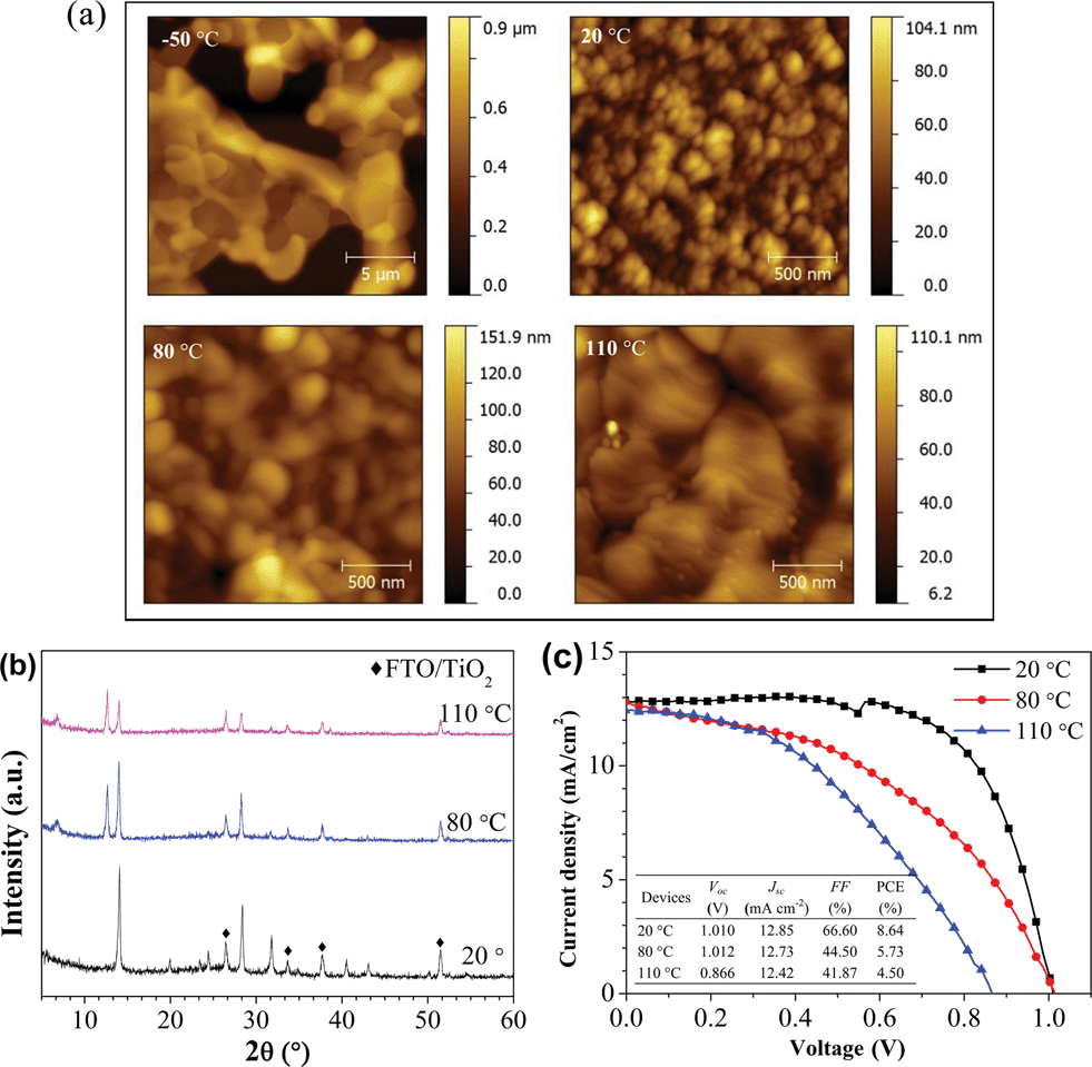 | ||
| Fig. 6 (a) AFM topography images of perovskite films grown on Si substrates at different substrate temperatures during the hybrid deposition from PbI2:MAI. The RMS roughness values are 209.9, 9.9, 20.1 and 13.1 nm for −50, 20, 80 and 110 °C of substrate temperatures, respectively. (b) XRD spectra of perovskite films grown on TiO2/FTO substrates at different substrate temperatures. (c) J–V curves of the devices under 1 sun illumination employing perovskite films prepared at different substrate temperatures. The device structure is FTO/TiO2 (70 nm)/perovskite (110 nm)/spiro-MeOTAD (100 nm)/Au (100 nm). The table as the inset shows the photovoltaic parameters of the devices. | ||
The results described above suggest that the growth of the perovskite film is highly dependent on the substrate temperature. The drastic changes in the crystal structure and surface morphology as a function of substrate temperature are ascribed to the different sticking coefficients of MAI on the substrate. The sticking coefficient is defined as the fraction of the incident molecules from the source that actually adheres to the substrate, which is dependent on the evaporation source material, substrate temperature, surface properties, and evaporation rate.55,56 The low temperature leads to a high sticking coefficient of MAI to the substrate followed by the poor quality of the perovskite film with partial coverage. The substrate temperature of 20 °C helps the growth of the perovskite film with high crystallinity and complete coverage. At higher temperatures (>80 °C), it is difficult to form pure perovskite films with suitable stoichiometry because of a small sticking coefficient of MAI on the substrate, generating films with excess PbI2 and intermediate phase.
It is hard to make a working device from the perovskite film grown with the substrate temperature held at −50 °C because of the poor morphological properties. The performance of the devices employing the perovskite films prepared at different substrate temperatures is shown in Fig. 6(c). The device with the perovskite film grown at 20 °C exhibits the best performance, with a Voc of 1.010 V, a Jsc of 12.85 mA cm−2, a FF of 66.60%, and an overall PCE of 8.64% under 1 sun illumination. In the case of 80 °C, the decreased PCE is probably ascribed to the presence of PbI2, because PbI2 has a larger bandgap energy (Eg = 2.3 eV),57 resulting in the increase of series resistance and consequently the decrease in FF. In addition, the appearance of the intermediate phase of the perovskite complex at higher substrate temperature may also be responsible for the poor PCE. When further increasing the substrate temperature to 110 °C, Voc and FF become lower, which are ascribed to the poor phase purity and poor morphology of the perovskite film. Therefore, the optimized substrate temperature is 20 °C. Note that the thickness of the perovskite layer for the devices is ∼110 nm, i.e. only one third of the perovskite layer thickness in efficient solution-processed PSCs.4,11,51 When we increase the thickness of the perovskite layer (∼170 nm), the device shows a Voc of 1.098 V, a Jsc of 19.92 mA cm−2, a FF of 52.44%, and an overall PCE of 11.48%. The corresponding J–V curve can be seen in Fig. S6 ESI.†
Post-annealing effect
For the solution-based methods, the post-annealing process is needed for fabricating PSCs with high PCEs, because the conversion of the perovskite film from precursors of metal halides and MAI requires sufficient temperatures (e.g., 80–120 °C) to ensure the vaporization of solvent and crystallization of the perovskite material, as well as to obtain uniform coverage.18,33 However, for the vacuum-based method, high performing PSCs were fabricated by either performing the post-annealing14,22 or skipping the post-annealing procedure in the reports.21,42 The necessity and the role of the post-annealing in the properties of perovskite films prepared by the vacuum-based method, as well as device performance are still lacking. A more systematic study is beneficial for fabricating PSCs with higher PCE. Therefore, we studied the post-annealing effects as a function of annealing temperature and annealing time on perovskite films prepared by the hybrid deposition method.First, the post-annealing studies were performed on non-stoichiometric perovskite films (see Fig. S7 of ESI†). The results suggest that post-annealing is beneficial on the perovskite films with excess MAI. When the annealing temperature is lower than 110 °C, the influence is negligible. Gentle annealing at 110–120 °C helps to desorb the undesirable H2O-incorporated complex from the perovskite film. High temperature (>130 °C) will decompose CH3NH3PbI3 to PbI2.
The effect of post-annealing on the stoichiometric perovskite films was studied next. Fig. 7 shows the XRD spectra and AFM images of perovskite films with balanced stoichiometry prepared from PbI2:MAI before and after post-annealing at 120 °C for 1 h. The XRD features before and after annealing are nearly the same, suggesting that the annealing has a negligible effect on the crystallinity of the film. Also the morphology of the perovskite film does not change drastically after the post-annealing, as revealed in Fig. 7(b). The RMS roughnesses before and after annealing is 33.8 and 29.2 nm, respectively. The post-annealing treatment only results in a slight reduction in surface roughness.
 | ||
| Fig. 7 (a) XRD spectra and (b) AFM topography images of the stoichiometric perovskite films prepared from PbI2:MAI before and after the post-annealing treatments at 120 °C for 1 h. The RMS roughness values before and after annealing are 33.8 and 29.2 nm, respectively. | ||
The results above suggest that the effect of post-annealing on the crystal structure and morphology of perovskite films with balanced stoichiometry is negligible. Also the device performance was approximately the same with or without post-annealing. This is drastically different from that of solution-processed samples,33,51 where the perovskite film properties and the device performances are strongly dependent on the post-annealing conditions. The results indicate that the hybrid deposition method allows the fabrication of PSCs at lower-temperatures (e.g. room temperature).
Semi-transparent PSCs
The BIPV system is very attractive for modern buildings. Integration of semi-transparent solar cells into BIPV windows is of particular interest, because it not only provides an aesthetic outlook, but also harvests solar energy to generate electricity power without extra installation space.58–61 Most of the perovskite cells made by solution-methods show a dark brownish hue – unappealing to architects who design skyscrapers. On the other hand, perovskite films prepared by the hybrid deposition method are semi-transparent. Comparison of perovskite films prepared by the solution and the hybrid deposition methods is shown in Fig. S8 ESI.†In addition, the presence of several hundred nanometer thickness of the spiro-MeOTAD HTL layer (250–600 nm)29,32,33,62 in a solution-based method leads to parasitic absorption loss, reducing further the overall transparency and ultimately limiting its BIPV application.63 However, the thickness of the spiro-MeOTAD HTL layer can be reduced to as thin as 100 nm in our device fabrication, since the perovskite layer prepared by the hybrid deposition method shows a very flat surface and the 100 nm-thick spiro-MeOTAD HTL layer can completely cover the perovskite layer to avoid the direct contact between the top Au layer and the perovskite layer. The transmittance of the 100 nm-thick spiro-MeOTAD HTL layer is shown in Fig. S9 ESI,† which exhibits extremely high transparency in the visible range. Therefore, the spiro-MeOTAD HTL layer does not induce the loss of transparency in the device. Fig. 8 shows a photograph of the PSC with 8.6% PCE prepared under optimized conditions, and the transmittance spectrum of the device without a top Au electrode. Visibly, the PSC also exhibits semi-transparency. Including the glass substrate, the average transmittance of this semi-transparent PSC is 40% in the range of 400–900 nm.
 | ||
| Fig. 8 Transmittance spectrum through the device acquired on an Au electrode-free region. The transmittance values include the glass substrate. The average transmittance in the range of 400–900 nm is 40%. The picture as the inset is a photograph of the semi-transparent PSC with 8.6% PCE prepared by the hybrid deposition method at room temperature. | ||
Our PSC can generate significant power while still having good transparency, allowing for the integration of semi-transparent solar cells into windows of buildings. For example, “if 6% efficient window photovoltaics (PVs) were used to cover a building the size of the Willis Tower in Chicago, the glass alone would generate nearly 5.3 gigawatt-hours of energy per year”, as stated by Service.46 The implementation of semi-transparent electrodes, such as Ag grids, Ag nanowires, ITO, graphene and carbon nanotubes64−69 is expected to achieve fully semi-transparent PSCs. Additionally, the perovskite layer thickness dependence results (as summarized in Table S1 of ESI†) indicate the good reproducibility of our hybrid deposition method for fabricating semi-transparent PSCs with high performance.
Conclusions
In summary, instrumentation and methodology for hybrid deposition were developed to overcome the difficulties generally faced by the vacuum-based methods by precisely controlling the MAI flow and the deposition rate of metal halides. Perovskite films prepared by this hybrid deposition method show very smooth surface, good crystallinity, full coverage with a small density of defects such as pin-holes, uniform chemical composition across the film thickness and semi-transparency. The study of the effects of different metal halides (PbCl2 or PbI2) shows that the chemical reactions between metal halides and MAI are very sensitive to the relative rate ratio of the evaporation materials. The crystallinity of lead-halide perovskite films shown by XRD is different when using different metal halides. In the PbCl2:MAI case, the perovskite films are much more oriented than the case of PbI2:MAI. This probably stems from the slow reaction speed by the presence of MACl in the PbCl2:MAI growth case. The substrate temperature during perovskite growth mainly affects the sticking coefficient of MAI. By increasing the substrate temperature, the sticking coefficient of MAI decreases. Perovskite films formed with non-stoichiometric ratios between metal halides and MAI showed always detrimental effects on the device performance. The optimized substrate temperature is 20 °C. In addition, it was found that the post-annealing treatment has negligible influence on the properties of the stoichiometric perovskite films and device performances, suggesting that the post-annealing is not a necessary step for fabricating PSCs by our hybrid deposition method. In this regard, the hybrid deposition method is very compatible with a low-temperature process for a flexible substrate to fabricate PSCs. Under optimized conditions, the PCE of PSC can be as high as 11.5%. This work indicates that the hybrid deposition method is very effective to prepare thin perovskite films with ultra-flat surface and fabricate PSCs with high performance.
Acknowledgements
This work was supported by the funding from the Okinawa Institute of Science and Technology Graduate University. We also thank Professor David Cahen and Dr. Saar Kirmayer from the Weizmann Institute of Science in Israel for providing MAI for some initial tests.Notes and references
- M. Grätzel, Nat. Mater., 2014, 13, 838–842 CrossRef PubMed.
- J. H. Im, C. R. Lee, J. W. Lee, S. W. Park and N. G. Park, Nanoscale, 2011, 3, 4088–4093 RSC.
- A. Kojima, K. Teshima, Y. Shirai and T. Miyasaka, J. Am. Chem. Soc., 2009, 131, 6050–6051 CrossRef CAS PubMed.
- S. D. Stranks, G. E. Eperon, G. Grancini, C. Menelaou, M. J. Alcocer, T. Leijtens, L. M. Herz, A. Petrozza and H. J. Snaith, Science, 2013, 342, 341–344 CrossRef CAS PubMed.
- S. Bai, Z. Wu, X. Wu, Y. Jin, N. Zhao, Z. Chen, Q. Mei, X. Wang, Z. Ye, T. Song, R. Liu, S. T. Lee and B. Sun, Nano Res., 2014, 7, 1749–1758 CrossRef CAS.
- G. Xing, N. Mathews, S. Sun, S. S. Lim, Y. M. Lam, M. Grätzel, S. Mhaisalkar and T. C. Sum, Science, 2013, 342, 344–347 CrossRef CAS PubMed.
- J. Feng and B. Xiao, J. Phys. Chem. Lett., 2014, 5, 1278–1282 CrossRef CAS.
- C. C. Stoumpos, C. D. Malliakas and M. G. Kanatzidis, Inorg. Chem., 2013, 52, 9019–9038 CrossRef CAS PubMed.
- C. Wehrenfennig, G. E. Eperon, M. B. Johnston, H. J. Snaith and L. M. Herz, Adv. Mater., 2014, 26, 1584–1589 CrossRef CAS PubMed.
- F. Matteocci, L. Cinà, F. D. Giacomo, S. Razza, A. L. Palma, A. Guidobaldi, A. D'Epifanio, S. Licoccia, T. M. Brown, A. Reale and A. D. Carlo, Pro. Photovoltaics, 2014 DOI:10.1002/pip.2557.
- J. Burschka, N. Pellet, S. J. Moon, R. Humphry-Baker, P. Gao, M. K. Nazeeruddin and M. Grätzel, Nature, 2013, 499, 316–319 CrossRef CAS PubMed.
- J. H. Im, I. H. Jang, N. Pellet, M. Grätzel and N. G. Park, Nat. Nanotechnol., 2014, 9, 927–932 CrossRef CAS PubMed.
- N. G. Park, Mater. Today, 2015, 18, 65–72 CrossRef CAS PubMed.
- M. Liu, M. B. Johnston and H. J. Snaith, Nature, 2013, 501, 395–398 CrossRef CAS PubMed.
- O. Malinkiewicz, A. Yella, Y. H. Lee, G. M. Espallargas, M. Grätzel, M. K. Nazeeruddin and H. J. Bolink, Nat. Photonics, 2014, 8, 128–132 CrossRef CAS PubMed.
- H. Zhou, Q. Chen, G. Li, S. Luo, T. B. Song, H. S. Duan, Z. Hong, J. You, Y. Liu and Y. Yang, Science, 2014, 345, 542–546 CrossRef CAS PubMed.
- M. A. Green, K. Emery, Y. Hishikawa, W. Warta and E. D. Dunlop, Prog. Photovoltaics, 2015, 23, 1–9 Search PubMed.
- A. Dualeh, N. Tetreault, T. Moehl, P. Gao, M. K. Nazeeruddin and M. Grätzel, Adv. Funct. Mater., 2014, 24, 3250–3258 CrossRef CAS PubMed.
- F. D. Giacomo, S. Razza, F. Matteocci, A. D'Epifanio, S. Licoccia, T. M. Brown and A. D. Carlo, J. Power Sources, 2014, 251, 152–156 CrossRef PubMed.
- L. Etgar, P. Gao, Z. Xue, Q. Peng, A. K. Chandiran, B. Liu, M. K. Nazeeruddin and M. Grätzel, J. Am. Chem. Soc., 2012, 134, 17396–17399 CrossRef CAS PubMed.
- O. Malinkiewicz, C. Roldán-Carmona, A. Soriano, E. Bandiello, L. Camacho, M. K. Nazeeruddin and H. J. Bolink, Adv. Energy Mater., 2014, 4, 1400345 Search PubMed.
- A. S. Subbiah, A. Halder, S. Ghosh, N. Mahuli, G. Hodes and S. K. Sarkar, J. Phys. Chem. Lett., 2014, 5, 1748–1753 CrossRef CAS.
- Q. Chen, H. Zhou, Z. Hong, S. Luo, H. S. Duan, H. H. Wang, Y. Liu, G. Li and Y. Yang, J. Am. Chem. Soc., 2014, 136, 622–625 CrossRef CAS PubMed.
- M. R. Leyden, L. K. Ono, S. R. Raga, Y. Kato, S. Wang and Y. Qi, J. Mater. Chem. A, 2014, 2, 18742–18745 CAS.
- C. W. Chen, H. W. Kang, S. Y. Hsiao, P. F. Yang, K. M. Chiang and H. W. Lin, Adv. Mater., 2014, 26, 6647–6652 CrossRef CAS PubMed.
- H. Hu, D. Wang, Y. Y. Zhou, J. L. Zhang, S. L. Lv, S. P. Pang, X. Chen, Z. H. Liu, N. P. Padture and G. L. Cui, RSC Adv., 2014, 4, 28964–28967 RSC.
- A. T. Barrows, A. J. Pearson, C. K. Kwak, A. D. F. Dunbar, A. R. Buckley and D. G. Lidzey, Energy Environ. Sci., 2014, 7, 2944–2950 CAS.
- Y. H. Hu, Adv. Mater., 2014, 26, 2102–2104 CrossRef CAS PubMed.
- J. M. Ball, M. M. Lee, A. Hey and H. J. Snaith, Energy Environ. Sci., 2013, 6, 1739–1743 CAS.
- T. Leijtens, B. Lauber, G. E. Eperon, S. D. Stranks and H. J. Snaith, J. Phys. Chem. Lett., 2014, 5, 1096–1102 CrossRef CAS.
- J. H. Heo, S. H. Im, J. H. Noh, T. N. Mandal, C. S. Lim, J. A. Chang, Y. H. Lee, H. Kim, A. Sarkar, K. NazeeruddinMd, M. Grätzel and S. I. Seok, Nat. Photonics, 2013, 7, 486–491 CrossRef CAS PubMed.
- M. M. Lee, J. Teuscher, T. Miyasaka, T. N. Murakami and H. J. Snaith, Science, 2012, 338, 643–647 CrossRef CAS PubMed.
- G. E. Eperon, V. M. Burlakov, P. Docampo, A. Goriely and H. J. Snaith, Adv. Funct. Mater., 2014, 24, 151–157 CrossRef CAS PubMed.
- Y. Nakayama, T. L. Nguyen, Y. Ozawa, S. Machida, T. Sato, H. Tokairin, Y. Noguchi and H. Ishii, Adv. Energy Mater., 2014, 4, 1301354 Search PubMed.
- Z. B. Wang, M. G. Helander, M. T. Greiner, J. Qiu and Z. H. Lu, Appl. Phys. Lett., 2009, 95, 043302 CrossRef PubMed.
- W. B. Chen, H. F. Xiang, Z. X. Xu, B. P. Yan, V. A. L. Roy, C. M. Che and P. T. Lai, Appl. Phys. Lett., 2007, 91, 191109 CrossRef PubMed.
- B. Lussem, M. Riede and K. Leo, Phys. Status Solidi A, 2013, 210, 9–43 CrossRef PubMed.
- Z. Xiao, Q. Dong, C. Bi, Y. Shao, Y. Yuan and J. Huang, Adv. Mater., 2014, 26, 6503–6509 CrossRef CAS PubMed.
- T. Salim, S. Sun, Y. Abe, A. Krishna, A. C. Grimsdale and Y. M. Lam, J. Mater. Chem. A, 2015, 3, 8943–8969 CAS.
- J. H. Kim, S. T. Williams, N. Cho, C. C. Chueh and A. K. Y. Jen, Adv. Energy Mater., 2015, 5, 1401229 Search PubMed.
- Q. Wang, Y. Shao, Q. Dong, Z. Xiao, Y. Yuan and J. Huang, Energy Environ. Sci., 2014, 7, 2359–2365 CAS.
- L. K. Ono, S. Wang, Y. Kato, S. R. Raga and Y. Qi, Energy Environ. Sci., 2014, 7, 3989 CAS.
- H. Yu, F. Wang, F. Xie, W. Li, J. Chen and N. Zhao, Adv. Funct. Mater., 2014, 24, 7102–7108 CAS.
- S. T. Williams, F. Zuo, C. C. Chueh, C. Y. Liao, P. W. Liang and A. K. Y. Jen, ACS Nano, 2014, 8, 10640–10654 CrossRef CAS PubMed.
- A. Poglitsch and D. Weber, J. Phys. Chem. Lett., 1987, 87, 6373–6378 CAS.
- J. H. Noh, S. H. Im, J. H. Heo, T. N. Mandal and S. I. Seok, Nano Lett., 2013, 13, 1764–1769 CAS.
- A. Wakamiya, M. Endo, T. Sasamori, N. Tokitoh, Y. Ogomi, S. Hayase and Y. Murata, Chem. Lett., 2014, 43, 711–713 CrossRef CAS.
- T. W. Ng, C. Y. Chan, M. F. Lo, Z. Q. Guan and C. S. Lee, J. Mater. Chem. A, 2015, 3, 9081–9085 CAS.
- N. Kitazawa, Y. Watanabe and Y. Nakamura, J. Mater. Sci., 2002, 37, 3585–3587 CrossRef CAS.
- Y. Zhao and K. Zhu, J. Phys. Chem. C, 2014, 118, 9412–9418 CAS.
- S. R. Raga, M.-C. Jung, M. V. Lee, M. R. Leyden, Y. Kato and Y. Qi, Chem. Mater., 2015, 27, 1597–1603 CrossRef CAS.
- R. J. Kennedy, R. Madden and P. A. Stampe, J. Phys. D: Appl. Phys., 2001, 34, 1853–1861 CrossRef CAS.
- A. R. Patel and D. Lakshminarayana, Thin Solid Films, 1982, 98, 59–63 CrossRef CAS.
- B. Borer, A. Sonnenfeld and P. R. V. Rohr, Surf. Coat. Technol., 2006, 201, 1757–1762 CrossRef CAS PubMed.
- K. Tu, J. W. Mayer and L. C. Feldman. Electronic Thin Film Science for Electrical Engineering and Materials Scientists, Macmillan: New York, 1992 Search PubMed.
- M. Rose, J. W. Bartha and I. Endler, Appl. Surf. Sci., 2010, 256, 3778–3782 CrossRef CAS PubMed.
- A. F. da Silva, N. Veissid, C. Y. An, I. Pepe, N. B. de Oliveira and A. V. B. da Silva, Appl. Phys. Lett., 1996, 69, 1930–1932 CrossRef PubMed.
- C. Zomer, A. Nobre, P. Cassatella, T. Reindl and R. Rüther, Prog. Photovoltaics, 2014, 22, 744–756 Search PubMed.
- Y. T. Chae, J. Kim, H. Park and B. Shin, Appl. Energy, 2014, 129, 217–227 CrossRef CAS PubMed.
- G. E. Eperon, V. M. Burlakov, A. Goriely and H. J. Snaith, ACS Nano, 2014, 8, 591–598 CrossRef CAS PubMed.
- R. F. Service, Science, 2014, 344, 458 CrossRef PubMed.
- H. S. Kim, C. R. Lee, J. H. Im, K. B. Lee, T. Moehl, A. Marchioro, S. J. Moon, R. Humphry-Baker, J. H. Yum, J. E. Moser, M. Grätzel and N. G. Park, Sci. Rep., 2012, 2, 591 Search PubMed.
- C. Roldan-Carmona, O. Malinkiewicz, R. Betancur, G. Longo, C. Momblona, F. Jaramillo, L. Camacho and H. J. Bolink, Energy Environ. Sci., 2014, 7, 2968–2973 CAS.
- T. Ameri, G. Dennler, C. Waldauf, H. Azimi, A. Seemann, K. Forberich, J. Hauch, M. Scharber, K. Hingerl and C. J. Brabec, Adv. Funct. Mater., 2010, 20, 1592–1598 CrossRef CAS PubMed.
- J. H. Yim, S.-Y. Joe, C. Pang, K. M. Lee, H. Jeong, J.-Y. Park, Y. H. Ahn, J. C. de Mello and S. Lee, ACS Nano, 2014, 8, 2857 CrossRef CAS PubMed.
- J. Huang, G. Li and Y. Yang, Adv. Mater., 2008, 20, 415–419 CrossRef CAS PubMed.
- Y. Y. Lee, K. H. Tu, C. C. Yu, S. S. Li, J. Y. Hwang, C. C. Lin, K. H. Chen, L. C. Chen, H. L. Chen and C. W. Chen, ACS Nano, 2011, 5, 6564–6570 CrossRef CAS PubMed.
- W. Gaynor, G. F. Burkhard, M. D. McGehee and P. Peumans, Adv. Mater., 2011, 23, 2905–2910 CrossRef CAS PubMed.
- J. V. D. Lagemaat, T. M. Barnes, G. Rumbles, S. E. Shaheen, T. J. Coutts, C. Weeks, I. Levitsky, J. Peltola and P. Glatkowski, Appl. Phys. Lett., 2006, 88, 233503 CrossRef PubMed.
Footnote |
| † Electronic supplementary information (ESI) available. See DOI: 10.1039/c5ta03593g |
| This journal is © The Royal Society of Chemistry 2015 |