
 Open Access Article
 This Open Access Article is licensed under a
 Creative Commons Attribution 3.0 Unported Licence
Large formamidinium lead trihalide perovskite solar cells using chemical vapor deposition with high reproducibility and tunable chlorine concentrations†
Matthew R.
Leyden
,
Michael V.
Lee
,
Sonia R.
Raga
and
Yabing
Qi
*
Energy Materials and Surface Sciences Unit (EMSS), Okinawa Institute of Science and Technology Graduate University (OIST), 1919-1 Tancha, Onna-son, Okinawa 904-0495, Japan. E-mail: Yabing.Qi@OIST.jp
First published on 29th June 2015
Abstract
Chemical vapor deposition is an inexpensive way to batch-process solar cells with good uniformity and facilitates low-cost production. Formamidinium lead iodide perovskite has a smaller energy band gap and greater potential efficiency than the widely studied methylammonium lead iodide perovskite and better temperature stability. This work is the first demonstration of vapor deposition of formamidinium-based perovskite. A self-limiting perovskite formation process is recommended, with efficiencies as high as 14.2% and stability up to 155 days after fabrication. Using this process, a batch of semi-transparent solar cells with a large area of 1 cm2 was fabricated. We monitored the growth of perovskite in real time and provide insight that may not be accessible for a solution based process. We directly measured chlorine in perovskite films and correlated the concentration of chlorine with efficiency and stability.
Introduction
The world uses ∼12.5 terawatt of energy and approximately 80% of it comes from fossil fuels such as oil, coal, and gas.1 Due to the rapidly declining costs of silicon solar cell production, the cost of photovoltaic electricity has reached parity with grid energy in many parts of the world.2 Solar energy production should now be viewed as cost-competitive, in addition to having a carbon footprint an order of magnitude lower than fossil fuel technologies.1 The field of organometal halide perovskite solar cells (PSCs) is rapidly growing,3 and low-temperature processing and low-cost materials promise to further reduce the cost per watt. PSCs have demonstrated up to 20.2% efficiency,4 which is competitive with commercial silicon solar cells, and have demonstrated solar areas up to 100 cm2 with 4.3% efficiency.5 PSCs have been fabricated by a variety of methods such as spin coating,6,7 vapor assisted solution process,8 blade coating,9 slot die,10 dual-source vapor deposition,11 hybrid deposition,12 chemical vapor deposition (CVD),13 spray coating,14etc. Some of these, like spin-coating, may be difficult to scale up, while CVD is used for a wide variety of industrial processes.15,16 Perovskite materials have the general formula of ABX3 and a wide variety of PSCs have been reported. Typically, the A component is methyl ammonium or formamidinium. B is a metal, such as lead or tin, and X is a halide, typically chlorine, iodine, or bromine. This work shows that formamidinium iodide (FAI)-based perovskite is a promising alternative to the widely studied methylammonium-based perovskite for solar cell applications. Solar cells typically need to operate under high temperature conditions, and FAI perovskite's improved temperature stability will facilitate a longer lifetime.17 Furthermore, the smaller energy band gap of ∼1.5 eV of FAI solar cells has a broader absorption band and potentially better performance. The current record PSC uses FAI containing perovskite.4 To date, almost all solar cells made with FAI have been prepared using a solution process.17–28 CVD offers an inexpensive way to scale-up PSCs because it is amenable to batch-processing. In addition to a higher throughput, batch processing can improve sample-to-sample uniformity. The self-limiting nature of perovskite formation by CVD improves batch-to-batch reproducibility. Furthermore, because perovskite growth is performed at temperatures commonly used for annealing, no additional annealing step is required, which improves reproducibility and reduces equipment requirements. This work is the first demonstration of fabrication of FAI-based PSCs using CVD that are stable even after 155 days, with efficiencies as high as 14.2%. Solar cells with areas as large as 1 cm2 provide efficiencies reaching 7.7%.Results and discussion
Perovskite solar cells fabricated by CVD
Perovskite was formed in a 2-step process, in which a thin film of lead halide was first deposited onto substrates pre-deposited with a TiO2 blocking layer. These substrates were loaded into one zone of a CVD tube furnace and FAI was loaded into a separate zone (Fig. 1a). The tube was then evacuated and purged with dry nitrogen. Substrates were first ramped up to 160 °C. Thereafter, the FAI source material was heated to 180 °C, causing it to sublimate. Typically, PbCl2 is thermally evaporated to a thickness of 100 nm. Upon full saturation with FAI, the film thickness increased from 103 ± 2 nm (PbCl2) to 324 ± 6 nm (perovskite). A completed solar cell would be coated with a hole transport layer made of spiro-MeOTAD, and would have gold top contacts (Fig. 1b).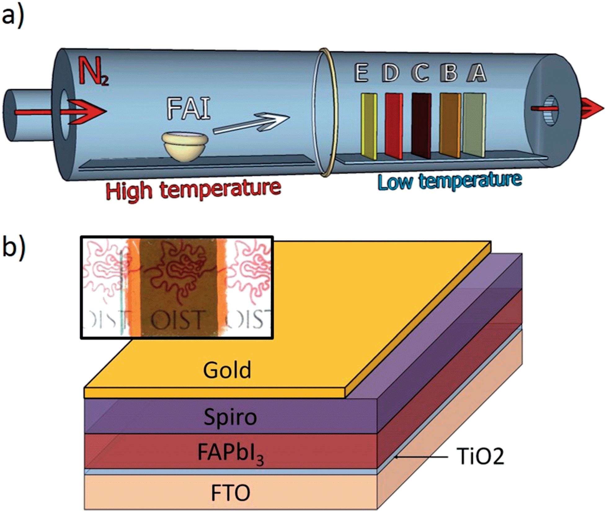 | ||
| Fig. 1 Schematic of perovskite growth and device structure. (a) Schematic of a chemical vapor deposition system for the growth of perovskite on substrates pre-deposited with PbCl2. (b) Diagram of the layered structure of a completed perovskite solar cell. The inset is a photograph of a 1 cm2 completed cell with a thin transparent gold top contact. | ||
FAI deposition
Under these growth conditions, FAI deposition appears to be largely mass transport-limited, meaning that the rate of conversion from PbCl2 to perovskite is limited by the amount of FAI transported to the substrate in the vapor phase. The amount of FAI deposited onto a substrate is dependent on a number of factors, such as the temperature of the FAI crucible, deposition time, surface area of the FAI, position, orientation, and packing density of substrates within the CVD. All of these factors were observed to affect growth and can be well controlled in a CVD process. Position dependence is more noticeable at lower temperatures (i.e. 120 °C), where substrates along the length of the CVD tube furnace develop a variety of colors despite having experienced the same nominal process (Fig. 2a and ESI video†). All positions transited all of the phases shown, (E–A), as long as the CVD process was allowed to progress. Improved uniformity is observed at temperatures above ∼145 °C, due to the inability of FAI to condense onto the sidewalls of the tube. This prevents formation of steep concentration gradients of FAI vapor below its sublimation temperature (∼145 °C). Therefore, it is possible to perform depositions on plastic substrates as long as the plastics maintain their integrity at the temperature used. Lower temperatures may require a temperature gradient, creating a reaction rate gradient that accommodates the concentration gradient. All devices were grown at 160 °C to ensure that substrates were well above the FAI sublimation temperature and to maximize rates of reaction and crystal growth. Growth was observed in situ and was recorded. Videos showing this growth are included in the ESI.†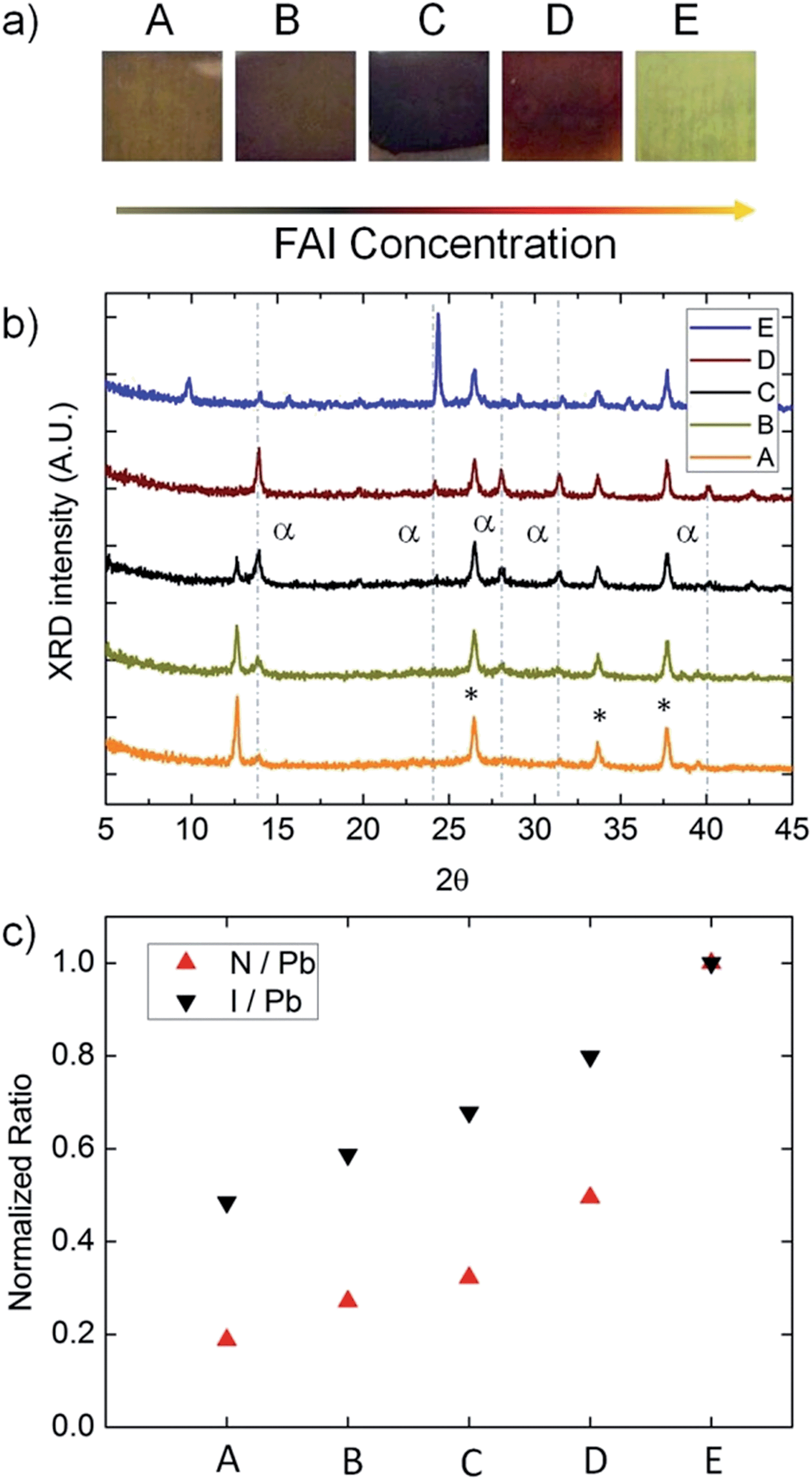 | ||
| Fig. 2 Phases of FAI-based perovskite growth. (a) Photographs of films on FTO glass at different stages of perovskite growth caused by an FAI concentration gradient. The thickness of the films from A to E was measured to be 117, 133, 161, 278, and 489 nm. (b) X-ray diffraction spectra of samples A–E. Crystal peaks originating from trigonal P3m1 perovskite are identified with an α and a dashed line. Peaks from the substrate are marked with a star (*). (c) X-ray photoelectron spectra (XPS) of samples A–E. This graph shows XPS intensity of iodine and nitrogen peaks relative to lead peaks, normalized to sample E. These spectra show that the concentrations of iodine and nitrogen increase from A to E. This confirms that the different samples correspond to different concentrations of FAI and the concentration of FAI is responsible for the different phases. | ||
Phases of perovskite film growth
During CVD growth, there are three possible phases of the thin film, depending on the amount of FAI deposited. First, PbCl2 is mostly converted to lead iodide, this is consistent with the yellow color, the appearance of an X-ray diffraction (XRD) peak at 12.6° (Fig. 2b), and the X-ray photon spectroscopy (XPS) measurement of the lead to iodide ratio of approximately 2![[thin space (1/6-em)]](https://www.rsc.org/images/entities/char_2009.gif) :1 (Fig. S1†).
:1 (Fig. S1†).
At higher concentrations of FAI, the film begins to form perovskite and turns from yellow to black. XRD peaks form at 13.9°, 28.0°, and 31.5°. With enough FAI for complete conversion, the film appears red in color and XRD peaks at 24.4° and 40.2° appear. These 5 peaks are consistent with trigonal perovskite in the P3m1 space group.29 At this stage, there is a defined absorption edge at ∼830 ± 10 nm (1.50 eV) in the UV-vis spectrum (Fig. S2†).
With increasing FAI, the film becomes oversaturated. It transitions from red to yellow, and a new yellow crystal structure forms with peaks at 9.9°, 15.7°, and 29.1°. Adding even more FAI causes the film to become comparatively opaque and creates new peaks at 18.0°, 25.7°, 27.0°, and 30.7° (Fig. S3†). FAI powder measured by XRD was found to have prominent peaks at 18.5°, 25.8°, 36.5° and 44.4° (Fig. S3†). Based on XRD and UV-vis results, at least 2 lead–FAI-based crystal structures other than perovskite, δ-phase perovskite,27 or bulk FAI can form during the CVD process. It would be interesting to characterize the structure of these yellow phases in more detail, but that is beyond the scope of this study.
Again, under low temperature conditions there is a gradient in the FAI vapor concentration along the length of the CVD tube. Samples have progressively less FAI deposited with increasing distance from the FAI source (from E to A) (Fig. 1). XPS was performed to confirm that sample E has more FAI than sample A. From the XPS spectrum, it is possible to measure the relative ratios of iodine and nitrogen relative to lead. Because all nitrogen in the samples comes from FAI, the gradient in the FAI concentration in samples E–A is confirmed by XPS results (Fig. 2d) and the FAI concentration determines the phase.
FAI saturation and device performance
Five representative batches of solar cells were fabricated, each with variable FAI deposition and heating times. These batches represent differing levels of FAI absorbed into the perovskite film, or levels of “saturation”. The degree of saturation is determined by visually monitoring the growth in situ. Details of each run are provided in the ESI.† In the first batch, source FAI was kept at 180 °C for a short time, and consequently this batch is believed to have been slightly undersaturated with FAI and devices fabricated had an average efficiency of 10.5% ± 0.7% (Tables 1 and S1, Fig. 3, and ESI video†). To test the roles of packing density and orientation, FTO glass substrates were loaded vertically, otherwise the CVD process was kept the same. This batch had a lower average efficiency of 7.8% ± 1.3%, which is likely due to being highly undersaturated with FAI. This suggests that FAI deposition depends on how substrates are loaded; tightly packed substrates take a longer time to convert to perovskite than loosely packed samples.| V oc | J sc (mA cm−2) | FF | PCE (%) | |
|---|---|---|---|---|
| Highly undersaturated | 0.90 | 17.2 | 51 | 7.8 |
| Undersaturated | 0.97 | 19.5 | 56 | 10.5 |
| Saturated | 0.97 | 21.6 | 62 | 13.0 |
| Oversaturated | 0.99 | 20.4 | 57 | 11.5 |
| Highly oversaturated | 0.93 | 18.5 | 46 | 8.0 |
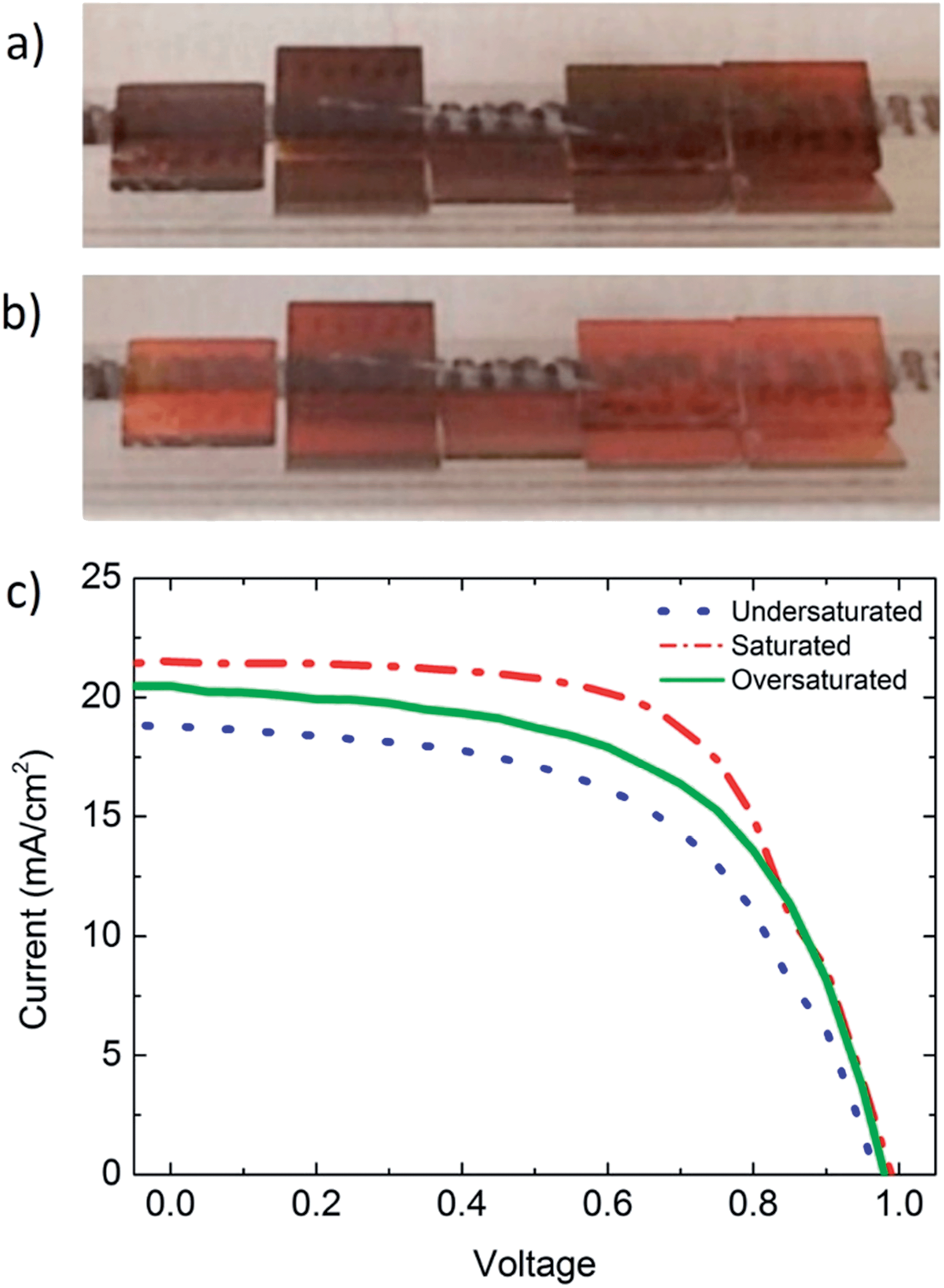 | ||
| Fig. 3 Impact of FAI saturation levels on the fill factor and Jsc. (a) Image from in situ monitoring of growth where substrates are saturated with FAI. (b) Image from the same growth, where substrates are oversaturated with FAI. (c) The graph shows representative I–V curves from three relevant batches. Changes in the saturation level primarily impact the fill factor and Jsc. The curves shown best represent the characteristics of the batch average, not the highest performing device. The active area of the representative curves is saturated 0.12 cm2, undersaturated 0.135 cm2, and oversaturated 0.04 cm2. | ||
A third batch was controlled by watching the batch and reducing the applied heat when substrates appeared to be saturated. This batch was completely saturated, but did not turn yellow like Fig. 2e, and showed the highest batch average efficiency of 13.0% ± 0.2%.
The perovskite formation process is reversible, in that films in the saturated yellow phase transitioned back to the perovskite phase when the FAI heat source was turned off and the substrate was kept at 160 °C (Fig. S3 and video†). This reversibility makes the CVD process more robust and easier to scale up, because it may be difficult to precisely control the amount of deposited FAI over the entire length of the CVD tube. A self-limiting desorption process ensures that substrates complete perovskite formation despite variations in saturation. A fourth batch was oversaturated with FAI, this growth was held at 160 °C for 1 h, which de-saturated the perovskite after the FAI heat source was turned off. This batch had an average efficiency of 11.5 ± 1.0%. A steady state measurement operating at 0.75 V was taken from the champion cell of this batch and gave a current density of 15 mA cm−2, corresponding to a PCE of 11.3% (Fig. S8†).
Large-area solar cells
A batch with high oversaturation was fabricated with an area of 1 cm2 and showed efficiencies as high as 7.7% (Fig. S5†). This efficiency was measured after 4 days of air exposure without encapsulation, which shows promise for long-term stability (∼23 °C and 40–50% relative humidity). The completed device (i.e. with Au top electrodes) was uniform in color and semi-transparent, demonstrating that PSCs made with CVD are compatible for applications such as solar windows.Grain size, phase history, and efficiency
One reason for the decreased efficiency of oversaturated perovskite is apparent from atomic force microscopy images of the surface morphology (Fig. 4). The apparent grain size of oversaturated batches is smaller (730 nm ± 360 nm) than that of saturated batches (970 nm ± 420 nm). Oversaturated samples likely have smaller grains because they must first convert from perovskite to the “yellow phase,” and then upon desorption of FAI, they must convert back to perovskite. This means that oversaturated films make comparatively larger changes in the crystal structure in roughly the same time as films that never converted to “yellow phase.” This decrease in size is more pronounced when films are highly oversaturated (500 nm ± 230 nm).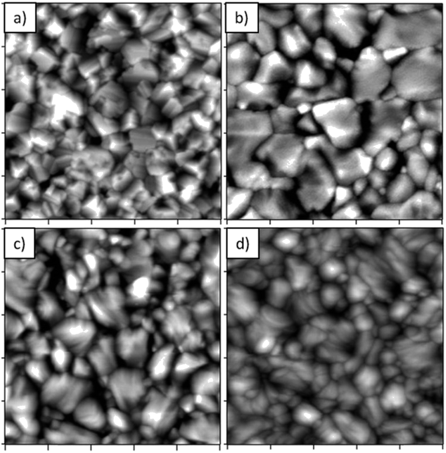 | ||
| Fig. 4 Oversaturation negatively impacts the grain size. Tapping-mode atomic force microscopy topography images of FAI perovskite films. All images are 5 μm × 5 μm with a Z range of 140 nm. (a) Undersaturated perovskite, deficient in FAI. Root-mean-square (RMS) roughness was 32 nm. (b) Saturated perovskite with 970 nm ± 420 nm grain size and RMS roughness of 36 nm. (c) Oversaturated and then de-saturated perovskite with a grain size of 730 nm ± 360 nm and a 32 nm RMS roughness. (d) Highly oversaturated and de-saturated perovskite with 500 nm ± 230 nm grains and 22 nm surface roughness. | ||
Chlorine concentration and efficiency
Despite the apparent conversion of PbCl2 to PbI2, samples grown with an initial PbI2 layer consistently had lower Voc and fill factors than samples made with PbCl2, even when samples were grown in the same CVD batch, or had similar grain sizes (Table S1 and Fig. S6†). This suggests that another mechanism related to chloride ions improves performance. In this study, chlorine was not directly detected by either XPS or XRD, but was detectable in time-of-flight secondary ion mass spectroscopy (ToF-SIMS). Perovskite samples similar to those formed in Fig. 2a were grown on glass, (labeled A2–E2 to differentiate this batch from previous samples on FTO). Samples A2, C2 and E2 were measured by ToF-SIMS (Fig. 5). All three samples showed insignificant numbers of chloride ions on the top surface, but significant numbers near the bottom for samples A2 and C2. Furthermore, chlorine measured near the bottom surface decreased with increasing FAI saturation. This is consistent with expectations because FAI is deposited on the top surface. Iodine first displaces chloride ions on the top and gradually proceeds down to the bottom. Also, with increasing amounts of iodine deposited, fewer chlorine atoms remain in the perovskite. Therefore, oversaturation depletes the concentration of chloride ions and provides an additional mechanism beyond the grain size that likely affects efficiency. It is possible that the chlorine ions in the less saturated films have improved carrier lifetime.30 By adjusting the degree of oversaturation, the chlorine concentration within the film can be tuned to optimize solar cell performance.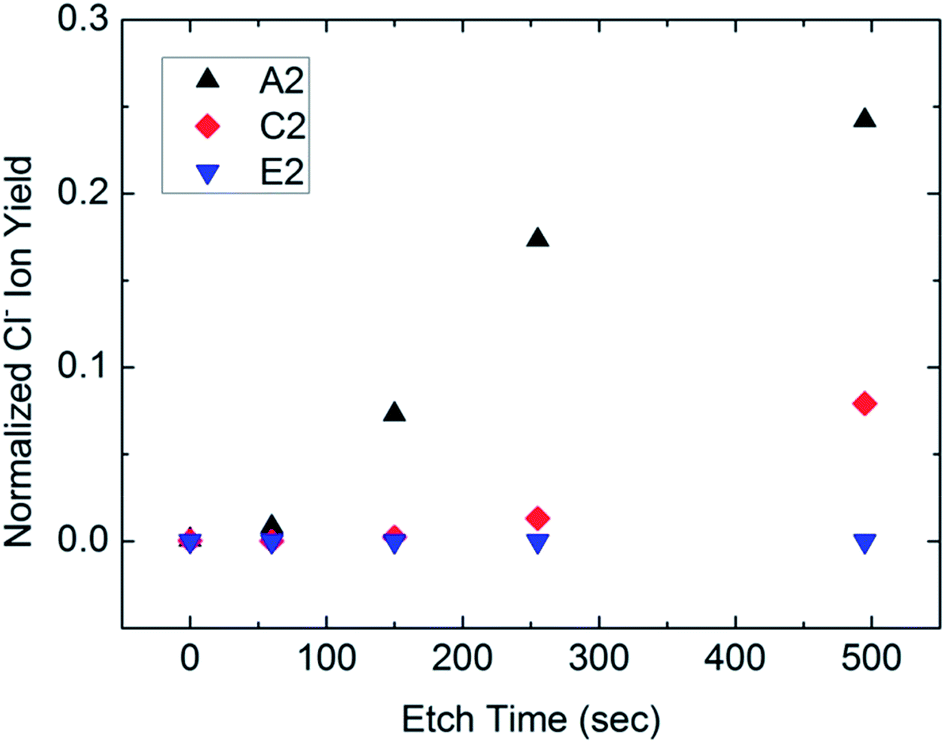 | ||
| Fig. 5 Chlorine concentration decreases with increasing saturation. The figure shows normalized chlorine counts from time of flight secondary ion mass spectroscopy as a function of etch times for three samples (A2, C2, and E2) with different levels of saturation. Etch time correlates with depth within the film, where 0 s represents the top surface and 500 s has reached the glass substrate. Chloride ions were not present in significant quantities on the top surface for all 3 samples. Samples A2 and C2 had chlorine concentrations that increase with increasing depth. Increasing levels of FAI saturation correlates with lower counts of chloride ions. For example, sample E2 which had the highest level of saturation had a negligible concentration of chlorine throughout the film. | ||
Stability
Temperature stability is important for all solar cells because they are required to operate under the heat of the sun. It is especially important for the CVD process because perovskite is grown at high temperatures. FAI is reported to have greater thermal stability than MAI.17 A simple test of MAI and FAI based perovskite films grown by CVD shows that the decay rate at 120 °C in air appears to be slower for FAI (Fig. 6).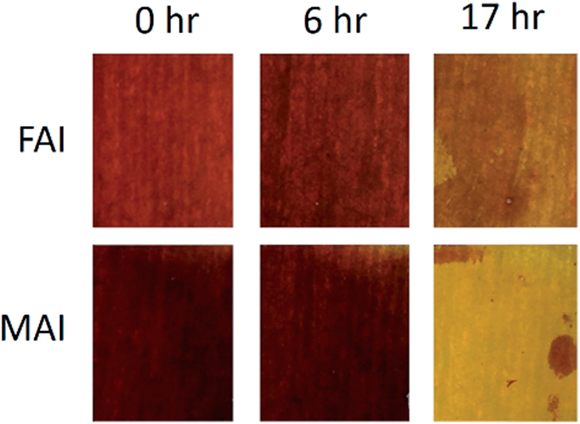 | ||
| Fig. 6 Perovskite films made with FAI are more thermally stable than MAI. Samples are left on a hot plate at 120 °C in air with ∼50% relative humidity. The MAI sample begins to decay at the edges after 6 h, while the FAI showed no sign of decay. After 17 h, the MAI film nearly completely decayed, while the FAI showed signs of decay but maintained a darker color. Perovskite films prepared on glass are approximately 300 nm thick. Photographs are taken with illumination from the bottom. | ||
A substrate with 4 samples from the “oversaturated” growth was chosen to monitor stability. Samples were stored in a nitrogen glovebox between measurements. The devices were found to be stable up to 155 days. The highest efficiency measurement of 14.2% was taken 42 days after fabrication. After 155 days, the average efficiency increased from 11.3% to 11.8%. Similarly, small improvements were observed previously with MAI-based perovskite cells made using CVD.13 This improvement in efficiency may be due to the improved charge transport properties of spiro-MeOTAD induced by air exposure,31 but the mechanism aside, the important issue is that the cells do not decay with time in an inert environment, which provides hope for stable cells with proper encapsulation (Table 2).
| Time | Sample | V oc | J sc (mA cm−2) | FF | PCE (%) |
|---|---|---|---|---|---|
| Fresh | Champion | 0.98 | 21.5 | 59 | 12.5 |
| Fresh | Average | 0.98 | 20.2 | 57 | 11.3 |
| 42 days | Champion | 1.03 | 20.9 | 66 | 14.2 |
| 104 days | Champion | 1.03 | 20.2 | 60 | 12.5 |
| 155 days | Champion | 1.02 | 21.8 | 60 | 13.4 |
| 155 days | Average | 1.02 | 19.9 | 58 | 11.8 |
Methods
Substrate preparation
FTO glass (Pilkington, 7 Ω/γ) was patterned by etching with Zn powder and 2 M HCl followed by brushing the surface with detergent, rinsing with deionized water, and sonication in 2-propanol. A compact layer of TiO2 was then deposited via spray pyrolysis using a precursor solution of acetylacetone, Ti(IV) isopropoxide, and anhydrous ethanol (3:3:2) on a pre-heated hot plate at 480 °C. This layer was approximately 65 nm thick (profilometer, Bruker).
Perovskite film growth by CVD
Perovskite films were grown in a two-step process where lead halide was first deposited onto substrates, followed by CVD deposition of FAI (Dyesol) which converted the film to perovskite. Unless stated otherwise, all perovskite films were prepared by depositing a 100 nm layer of lead chloride onto substrates by thermal evaporation (at 2.0 × 10⁻² Pa, approximately 0.1 to 0.4 Å s−1, using PbCl2 powder, Sigma-Aldrich). The thickness was monitored with a quartz-crystal microbalance and additionally measured using a profilometer. Substrates pre-deposited with PbCl2 were loaded into a 2-zone CVD furnace, where the first zone was loaded with ∼1 g of solid FAI powder and the second zone with substrates. For all devices reported in Fig. 3, substrates were ramped up to 160 °C, and then FAI was ramped to 180 °C. Essentially, all FAI absorption occurs when the substrate is at 160 °C. This temperature was measured with a thermocouple placed inside of the CVD tube to guarantee a temperature measurement similar to the substrate. All devices were grown in a 6 cm region between labels B and D marked on the CVD tube to maximize batch uniformity (Fig. 1). Total FAI sublimation time was approximately 30 min, where FAI was held at 180 °C for ∼6–16 min, and ∼20 min was required for ramp up and cool down. The amount of FAI consumed was typically ∼50 mg or less. FAI temperature was allowed to cool below 160 °C and substrate heating was turned off.Device fabrication
Solar cell device fabrication was completed by spin-coating a hole transport layer that consists of a mixture of three materials: spiro-MeOTAD (2,2′,7,7′-tetrakis(N,N-di-p-methoxy-phenylamine)-9,9′-spirobifluorene (Suna Tech Inc.) dissolved in chlorobenzene (70 mg mL−1), 20 μL of Li-bis(trifluoromethanesulfonyl)-imide (LiTFSI, Sigma) dissolved in acetronitrile (50 mg/100 μL), and 30 μL of tert-butylpyridine (t-BP, Sigma). Top electrodes were gold, deposited by thermal evaporation (<1.0 × 10⁻⁶ Torr, at 0.1–0.2 Å s−1) through a shadow mask. The nominal solar cell active area ranged from 0.04–0.169 cm2, in addition to one batch of solar cells of 1 cm2.ToF-SIMS measurements
Time of flight secondary ion mass spectrometry (ToF-SIMS) measurements were performed to study the role of chlorine. The Cl− ion signal was normalized based on its ratio to the total ion yield in negative ion extraction mode. Chlorine counts were binned from 34.92 to 35.02 amu. We thank ULVAC-PHI, Inc. for helping with ToF-SIMS measurements.Solar cell measurements
Current–voltage (I–V) characteristics of solar cells were measured under 1-sun illumination (AM 1.5 G, 100 mW cm−2) using a solar simulator (Newport Oriel Sol 1A) and a Keithley 2400 source meter. All measurements were performed without a mask, in ambient air at ∼23–25 °C and a relative humidity of ∼40–50%. All measurements were made with a sweep rate of ∼0.4 V s−1 with a range of −0.1 to 1.1 V, and 60 s of light pre-illumination.Film characterization
X-ray diffraction spectra were measured using a D8 Discover (Bruker). Atomic Force Microscopy images were taken using an Asylum MFP-3D in AC mode. UV-vis absorbance spectra were measured on a Jasco V-670 spectrometer. X-ray photoelectron spectroscopy was performed with an AXIS Ultra DLD (Kratos Analytical Ltd.) using monochromated Al Kα X-rays.Conclusions
Tight process control may be at odds with a cost-effective process. A more robust process demonstrating stability and reasonably high efficiency is more desirable. In the reversible process (i.e. oversaturation), desorption of FAI appears self-limiting, making the FAI oversaturation process both robust and convenient to control. This process produced uniform films along the length of the CVD tube and was easier to reproduce from batch to batch. By adjusting the degree of FAI oversaturation in the perovskite film, the chlorine content can be adjusted, subsequently changing performance and stability. This process demonstrated efficiencies as high as 14.2%, with a batch average of 11.5% ± 1.0%. Cells with sizes as high as 1 cm2 were fabricated by reversible formation, with future modules likely being limited only by the size of the CVD tube. Chlorine concentrations in perovskite films were studied by time-of-flight secondary ion mass spectroscopy and may play an important role in cell efficiency and stability.Acknowledgements
This work was supported by funding from the Energy Materials and Surface Sciences Unit of the Okinawa Institute of Science and Technology Graduate University. We thank ULVAC-PHI, Inc. for helping with ToF-SIMS measurements. We thank Steven D. Aird, the Technical Editor at Okinawa Institute of Science and Technology Graduate University for valuable suggestions in revising the manuscript.Notes and references
- M. M. Aman, K. H. Solangi, M. S. Hossain, A. Badarudin, G. B. Jasmon, H. Mokhlis, A. H. A. Bakar and S. N. Kazi, Renewable Sustainable Energy Rev., 2015, 41, 1190–1204 CrossRef CAS PubMed.
- M. Bazilian, I. Onyeji, M. Liebreich, I. MacGill, J. Chase, J. Shah, D. Gielen, D. Arent, D. Landfear and S. Zhengrong, Renewable Energy, 2013, 53, 329–338 CrossRef PubMed.
- N.-G. Park, Mater. Today, 2015, 18(2), 65–72 CrossRef CAS PubMed.
- W. S. Yang, J. H. Noh, N. J. Jeon, Y. C. Kim, S. Ryu, J. Seo and S. I. Seok, Science, 2015, aaa9272 Search PubMed.
- S. Razza, F. Di Giacomo, F. Matteocci, L. Cinà, A. L. Palma, S. Casaluci, P. Cameron, A. D'Epifanio, S. Licoccia, A. Reale, T. M. Brown and A. Di Carlo, J. Power Sources, 2015, 277, 286–291 CrossRef CAS PubMed.
- J. Burschka, N. Pellet, S.-J. Moon, R. Humphry-Baker, P. Gao, M. K. Nazeeruddin and M. Grätzel, Nature, 2013, 499, 316–319 CrossRef CAS PubMed.
- M. M. Lee, J. Teuscher, T. Miyasaka, T. N. Murakami and H. J. Snaith, Science, 2012, 338, 643–647 CrossRef CAS PubMed.
- Q. Chen, H. Zhou, Z. Hong, S. Luo, H.-S. Duan, H.-H. Wang, Y. Liu, G. Li and Y. Yang, J. Am. Chem. Soc., 2013, 136, 622–625 CrossRef PubMed.
- J. H. Kim, S. T. Williams, N. Cho, C.-C. Chueh and A. K.-Y. Jen, Adv. Energy Mater., 2015, 5, 1401229 Search PubMed.
- K. Hwang, Y.-S. Jung, Y.-J. Heo, F. H. Scholes, S. E. Watkins, J. Subbiah, D. J. Jones, D.-Y. Kim and D. Vak, Adv. Mater., 2015 DOI:10.1002/adma.201404598.
- M. Liu, M. B. Johnston and H. J. Snaith, Nature, 2013, 501, 395–398 CrossRef CAS PubMed.
- L. K. Ono, S. Wang, Y. Kato, S. R. Raga and Y. Qi, Energy Environ. Sci., 2014, 7, 3989–3993 CAS.
- M. R. Leyden, L. K. Ono, S. R. Raga, Y. Kato, S. Wang and Y. B. Qi, J. Mater. Chem. A, 2014, 2, 18742–18745 CAS.
- A. T. Barrows, A. J. Pearson, C. K. Kwak, A. D. F. Dunbar, A. R. Buckley and D. G. Lidzey, Energy Environ. Sci., 2014, 7, 2944–2950 CAS.
- J.-H. Park and T. S. Sudarshan, Chemical Vapor Deposition, ASM International, 2001 Search PubMed.
- X.-T. Yan and Y. Xu, Chemical Vapour Deposition: An Integrated Engineering Design for Advanced Materials, Springer Science & Business Media, 2010 Search PubMed.
- G. E. Eperon, S. D. Stranks, C. Menelaou, M. B. Johnston, L. M. Herz and H. J. Snaith, Energy Environ. Sci., 2014, 7, 982 CAS.
- N. Pellet, P. Gao, G. Gregori, T.-Y. Yang, M. K. Nazeeruddin, J. Maier and M. Grätzel, Angew. Chem., Int. Ed., 2014, 53, 3151–3157 CrossRef CAS PubMed.
- S. Pang, H. Hu, J. Zhang, S. Lv, Y. Yu, F. Wei, T. Qin, H. Xu, Z. Liu and G. Cui, Chem. Mater., 2014, 26, 1485–1491 CrossRef CAS.
- S. Lv, S. Pang, Y. Zhou, N. P. Padture, H. Hu, L. Wang, X. Zhou, H. Zhu, L. Zhang, C. Huang and G. Cui, Phys. Chem. Chem. Phys., 2014, 16, 19206 RSC.
- T. M. Koh, K. Fu, Y. Fang, S. Chen, T. C. Sum, N. Mathews, S. G. Mhaisalkar, P. P. Boix and T. Baikie, J. Phys. Chem. C, 2013, 118, 16458–16462 Search PubMed.
- M. Hu, L. Liu, A. Mei, Y. Yang, T. Liu and H. Han, J. Mater. Chem. A, 2014, 2, 17115–17121 CAS.
- F. C. Hanusch, E. Wiesenmayer, E. Mankel, A. Binek, P. Angloher, C. Fraunhofer, N. Giesbrecht, J. M. Feckl, W. Jaegermann, D. Johrendt, T. Bein and P. Docampo, J. Phys. Chem. Lett., 2014, 5, 2791–2795 CrossRef CAS.
- R. S. Sanchez, V. Gonzalez-Pedro, J.-W. Lee, N.-G. Park, Y. S. Kang, I. Mora-Sero and J. Bisquert, J. Phys. Chem. Lett., 2014, 5, 2357–2363 CrossRef CAS.
- S. Aharon, A. Dymshits, A. Rotem and L. Etgar, J. Mater. Chem. A, 2015, 3, 9171–9178 CAS.
- G. E. Eperon, V. M. Burlakov, A. Goriely and H. J. Snaith, ACS Nano, 2014, 8, 591–598 CrossRef CAS PubMed.
- N. J. Jeon, J. H. Noh, W. S. Yang, Y. C. Kim, S. Ryu, J. Seo and S. I. Seok, Nature, 2015, 517, 476–480 CrossRef CAS PubMed.
- J.-W. Lee, D.-J. Seol, A.-N. Cho and N.-G. Park, Adv. Mater., 2014, 26, 4991–4998 CrossRef CAS PubMed.
- C. C. Stoumpos, C. D. Malliakas and M. G. Kanatzidis, Inorg. Chem., 2013, 52, 9019–9038 CrossRef CAS PubMed.
- D. W. deQuilettes, S. M. Vorpahl, S. D. Stranks, H. Nagaoka, G. E. Eperon, M. E. Ziffer, H. J. Snaith and D. S. Ginger, Science, 2015, 348, 683–686 CrossRef CAS PubMed.
- Z. Hawash, L. K. Ono, S. R. Raga, M. V. Lee and Y. B. Qi, Chem. Mater., 2015, 27, 562–569 CrossRef CAS.
Footnote |
| † Electronic supplementary information (ESI) available. See DOI: 10.1039/c5ta03577e |
| This journal is © The Royal Society of Chemistry 2015 |