
 Open Access Article
 This Open Access Article is licensed under a Creative Commons Attribution-Non Commercial 3.0 Unported Licence
The rise of hematite: origin and strategies to reduce the high onset potential for the oxygen evolution reaction
Beniamino
Iandolo†
*,
Björn
Wickman
,
Igor
Zorić
and
Anders
Hellman
*
Department of Applied Physics, Chalmers University of Technology, SE-41296 Göteborg, Sweden. E-mail: anders.hellman@chalmers.se
First published on 18th June 2015
Abstract
Hematite (α-Fe2O3) has emerged as a promising material for photoelectrochemical (PEC) water splitting thanks to its abundance, stability in an aqueous environment, favorable optical bandgap and position of the electronic valence band. Nevertheless, its performance as a photoanode is considerably lower than what is theoretically achievable. In particular, the high electrochemical potential usually needed to initiate water oxidation is detrimental to the prospect of using hematite for practical devices. In this review we elucidate the appealing, as well as the challenging, aspects of using hematite for PEC water splitting and focus on the recent efforts towards lowering the onset potential of water oxidation. We examine and rationalize several strategies pursued to achieve this goal involving manipulation of the hematite/electrolyte interface, as well as improving relevant properties of hematite itself.
 Beniamino Iandolo | Dr Beniamino Iandolo obtained his Ph.D. in Physics from the Chalmers University of Technology, Sweden, in 2014. Research for his doctoral thesis centered on light-driven water splitting on hematite. He is currently a postdoctoral fellow at the Technical University of Denmark, where he scrutinizes novel materials for solar energy conversion and storage using environmental transmission electron microscopy. |
 Björn Wickman | Dr Björn Wickman is a postdoctoral fellow at Chalmers University of Technology, Sweden. He received his Ph.D. in Physics from Chalmers University of Technology in 2010. Dr Wickman has done postdoctoral studies at the Technical University of Denmark. His research interests center around electro- and photoelectrochemical solutions for energy and environmental applications. He has developed and evaluated well controlled, nanofabricated model systems to study reaction mechanisms in the fields of fuel cells, CO2 reduction, and water splitting. |
 Igor Zorić | Igor Zorić is a Professor Emeritus at the Department of Applied Physics, Chalmers University of Technology, Sweden. His work focuses on dynamics and kinetics of surface reactions, nanoplasmonics and photoelectrochemistry. |
 Anders Hellman | Anders Hellman is an Associate Professor at the Department of Applied Physics, Chalmers University of Technology, Sweden. He received his Ph.D. in Physics in 2003 from the University of Gothenburg, Sweden. Dr Hellman has done postdoctoral studies at Haldor Topsøe A/S, Technical University of Denmark, and at the Competence Centre for Catalysis, Sweden. He has worked on various topics related to surface science, heterogeneous catalysis and materials for energy harvesting, such as charge transfer and non-adiabaticity in surface reactions, ammonia synthesis, CO and methane oxidation, thin oxides supported on metals, and (photo)electrochemical studies of water splitting. |
Introduction
Fossil fuels account for about 87% of the global mean power consumption, which is currently about 16 terawatt (TW)1,2 and is expected to increase up to 30 TW by 2050.3,4 It follows that any technology for harvesting, converting and/or storing energy in a sustainable way must be scaled to the TW level in order to make an appreciable impact at a global scale. Solar energy is the most appealing candidate to solve this appropriately called “TW challenge”.5 More energy, in the form of sunlight, strikes the Earth in one hour than what society currently consumes in a year.6 However, sunlight is intermittent, i.e., it varies irregularly over the day, year, and place on earth, which implies that schemes and devices to store and release the harvested energy on demand are needed. An elegant approach to this problem consists in directly converting sunlight into chemical energy in the form of molecular bonds, i.e. producing fuels. Nature has already implemented such a scheme in biological photosynthesis, where sunlight converts CO2 and H2O into hydrocarbons and O2. However, since the overall efficiency of this process is low (about 1% at best),7,8 different routes towards artificial photosynthesis have received considerable attention.9 In particular, H2 production from H2O splitting has the potential to become the backbone of a hydrogen-based sustainable energy economy,10,11 given the abundance of H2O on Earth and that the only byproduct of H2 when consumed in a fuel cell is, once again, H2O.One can identify three types of devices to perform solar water splitting: (i) photovoltaic (PV) devices wired to H2O electrolyzers, (ii) photocatalytic cells, and (iii) photoelectrochemical (PEC) cells. The latter ones use solid-state electrodes in a similar way to conventional electrolyzers, where H2O oxidation (or O2 evolution reaction, OER) and reduction (H2 evolution reaction, HER) take place at two different solid/liquid junctions. In PEC cells, at least one of the electrodes consists of a semiconductor capable of absorbing the incoming light, and in which a depletion (or space-charge, SC) region is formed at equilibrium. The photogenerated charges are separated by the electric field in the SC region and travel to a solid/liquid junction where they take part in either the HER or the OER.
The key requirements of materials for high-efficiency PEC water splitting can be summarized as follows:
• Bandgap size that allows for broad light absorption.
• Quasi-Fermi energy levels for electrons and holes that straddle the HER and OER potential respectively.
• High yield of conversion of photogenerated charges into H2 and O2.
Moreover, the electrodes must be durable in the often harsh electrolytic environment and consist of earth abundant elements in view of process scalability. Despite the enormous effort since the seminal work on water splitting on TiO2,12,13 no single material that meets all these requirements has emerged so far.14,15 While much work is devoted to identify the ideal semiconductor for this purpose (also using combinatorial and/or ab initio calculations16–18), focus is increasingly shifting towards using two or more photoactive materials. A commonly investigated scheme involves coupling a semiconductor capable of carrying out one of the half-reactions to a PV device that supplies the bias needed to perform complete water splitting.14 III–V photocathodes in connection to a PV cell reach solar-to-hydrogen (STH) conversion efficiency over 12%,19 although cost and stability considerations have prevented these devices from attaining economic significance. Alternatively, a stable, inexpensive metal oxide can be used to perform the OER. Metal oxides commonly used within this scheme are TiO2,20–24 WO3,25–29 ZnO,30–33 BiVO4![[thin space (1/6-em)]](https://www.rsc.org/images/entities/char_2009.gif) 34–38 and Fe2O3.39–43
34–38 and Fe2O3.39–43
Fe2O3 (or iron(III) oxide, hematite) is of great interest thanks to its bandgap of ∼2.0 eV, which results in a theoretical maximum STH conversion efficiency of about 15%.44 However, the highest STH efficiency achieved so far is 3.1% using state-of-the-art hematite photoanodes,45 whereas more typically STH is of the order of about 1% or less.11 Clearly, much remains to be done in order to exploit the full potential of hematite. In this review, we briefly describe the properties of hematite of interest for PEC water splitting. Then, we focus on one of the factors limiting the performance of hematite, namely the highly anodic potential required to initiate the OER. We critically examine the advancements in alleviating the former issue, as well as review recent efforts in deepening the understanding of the OER on hematite.
Hematite for PEC water splitting
In the search for the ultimate semiconductor for PEC water splitting, hematite attracted interest almost four decades ago.46 This fact is not surprising given (i) that hematite can theoretically absorb up to 40% of solar radiation,47 (ii) that it shows excellent (photo)electrochemical stability in a pH range from 3 to 14,48 and (iii) that iron is the fourth most abundant element in the Earth's crust.2 Hematite is thermodynamically the most stable form of iron oxide, and all iron oxides can be transformed into hematite upon appropriate thermal treatment.49,50 In the following section, we briefly review the PEC properties of hematite. Then, we outline the challenges in exploiting the full potential of hematite as a photoanode.PEC properties
The optical and electronic properties of hematite have been thoroughly investigated and are summarized in recent reviews.51–53 The optical bandgap energy is reported between 1.9 and 2.2 eV (corresponding to wavelengths of 650 and 560 nm respectively) depending on the sample preparation technique.51 Tauc's analysis54 of the absorption coefficient indicates that the bandgap is indirect, i.e. phonon participation is necessary in the photoexcitation process. As a consequence, the absorption length α−1 in hematite is relatively long, for instance, α−1 = 118 nm at a photon wavelength of 550 nm.55In terms of electronic properties, hematite is described as a Mott insulator56 where charge transport takes place via polaron hopping,57,58 using models that include the effect of the size difference between Fe2+ and Fe3+ ions and the associated lattice distortion.59,60 Notably, the electron conduction within the (0001) basal plane is four orders of magnitude higher than in the perpendicular planes.61–63 Femtosecond laser spectroscopy studies of the excited states in hematite nanoparticles, thin films and single crystals reveal an ultra-fast dynamics, where hot electrons thermalize within 300 fs and recombine within 3 ps.64,65 Based on the short lifetime and low charge carrier mobility value,66 the diffusion length for holes LD is usually estimated to be between 1.5 and 5 nm.67,68
The OER involves four holes for each O2 molecule produced, with a characteristic time for a complete cycle as long as some seconds on hematite,69 and hence it is usually characterized as “slow” or “sluggish”. The microscopic mechanism of the OER on hematite is currently the subject of intense investigation.70–73 A few schemes involving different reaction intermediates have been proposed,39,69,74 and the recent review by Young et al.52 summarizes the advancement on the topic. The formation of some reaction intermediates such as Fe–O and Fe–OOH is consistent with the hypothesis that the OER proceeds via the trapping of holes at Fe species, and subsequent transfer of these holes to the electrolyte.74,75 These states are often referred to as surface states, and have been probed using several spectroscopic techniques such as electrochemical impedance spectroscopy (EIS),74,75 intensity modulated photocurrent spectroscopy (IMPS),76,77 light/potential modulated absorbance spectroscopy (LMAS/PMAS)78,79 and transient absorption spectroscopy (TAS).69,80 The surface states were initially regarded to act solely as recombination centers, with the OER proceeding via direct transfer of holes from the valence band. On the other hand, there is increasing evidence that the OER actually takes place from the same surface states, which therefore display an ambivalent nature. For instance, thanks to a combination of first-principle calculations and PEC measurements on polycrystalline hematite thin films, it was demonstrated that the surface states act as recombination centers for potentials more cathodic than the onset potential, Vonset, while as states through which the OER takes place for potentials more anodic than Vonset.81
Challenges
Fig. 1a shows a schematic energy diagram of a PEC water splitting device based on a hematite photoanode and a metallic cathode. Photons with energy equal to or larger than the bandgap energy EG are absorbed with efficiency ηe−/h+. The quasi-Fermi energy levels for electrons and holes are indicated as EF,n and EF,p, respectively. The difference between the two equals the photovoltage sustained by hematite, Vph. The built-in electric field extends throughout the depletion region (characterized by a length WSC) and drives holes towards the hematite/electrolyte junction and electrons to the cathode via an electron collector and an external circuit. The flat band potential Vfb of hematite (not shown here) is the potential at which there is no built-in field and therefore no band bending in the semiconductor. ηtr is the fraction of photogenerated charges reaching the respective solid/liquid interface. Then, holes are transferred to the electrolyte with efficiency ηct, and take part in the OER. The overall STH efficiency of the device is determined by the following: (i) charge generation efficiency ηe−/h+; (ii) charge transport efficiency ηtr; (iii) charge transfer efficiency ηct; (iv) oxidative power of holes; (v) reducing power of electrons.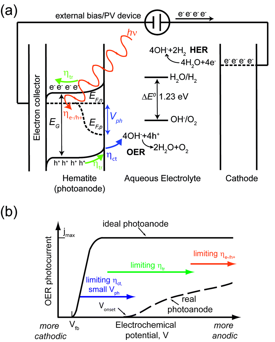 | ||
| Fig. 1 (a) Schematic energy diagram of a PEC device based on a hematite photoanode. Photons with energy equal to or larger than the bandgap in hematite EG are absorbed with efficiency ηe−/h+. The built-in electric field in hematite drives holes towards the hematite/electrolyte junction and electrons to the cathode (usually via a charge collector and an external circuit). ηtr is the fraction of photogenerated charges reaching the respective solid/liquid interface. Holes are transferred to the electrolyte with efficiency ηct, and take part in the OER. An external bias/PV device supplies electrons with sufficient energy so that they take part in the HER. (b) PEC performance gap between a state-of-the-art photoanode and the ideal hematite-based photoanode. The former (dashed line) shows an OER Vonset between 1.0 and 1.1 V vs. RHE and slowly reaches a maximum photocurrent jmax of 4 mA cm−2 at 1.5 V vs. RHE. In the latter (solid line), Vonset = Vfb (typically 0.5 V vs. RHE) and a jmax of 12 mA cm−2 is reached within 0.1 V. The arrows indicate the main performance limiting factor for increasingly anodic potential: first charge transfer at the hematite/electrolyte interface and the small photovoltage, then charge transport within hematite, finally photon absorption in the semiconductor. | ||
Achieving high ηe−/h+ and ηtr simultaneously is challenging given the mismatch between α−1 and WSC + LD.82–84 While the electron conductivity can be increased by introducing dopant atoms (at levels of around a few percent) with higher valence than 3+ (ref. 85–98) or oxygen vacancies,99 even in a heavy doping regime α−1 ≫ WSC + LD, since WSC shortens for increasing dopant concentration.100 Fabrication of nanostructured electrodes has shown to be effective in alleviating this mismatch, and a plethora of morphologies has been demonstrated in the last decade.41,95,101–114 Another promising strategy consists in employing ultrathin (i.e. thickness smaller than 50 nm) hematite films and enhancing ηe−/h+ through improving photon management by depositing hematite on top of a reflecting surface,115 or by sensitizing it with nanostructures supporting plasmonic resonances.116–123
η ct is normally close to unity only when a high anodic potential is applied to hematite, due to the slow OER kinetics mentioned above. Moreover, Vph is usually much lower than the theoretical maximum. For heavily doped hematite, ideally, EF,n lies just below the bottom of the conduction band and Vph almost equals the optical bandgap, leaving EF,p just above the top of the valence band. Unfortunately, this is far from being the case for hematite, where Vph is typically smaller than 0.4 eV.124 We emphasize that the small Vph is largely overlooked when considering the performance-limiting factors of hematite, since it is often assumed that the latter is an excellent candidate for the OER based on the consideration that the top of the valence band lies about 0.7 eV below the OER potential.53
Finally, UV photoelectron spectroscopy indicates that the bottom of the conduction band lies 0.1–0.2 eV lower than the HER potential.125 Therefore, even for heavily n-doped hematite where the quasi-Fermi for electrons in EF,n lies just below the bottom of the conduction band, complete water splitting using hematite as a single photoabsorber cannot take place without an external bias.14,126–128
Focusing on the OER half-cell reaction (and therefore neglecting here overpotentials and other issues associated with the HER), the non-idealities mentioned above result in a considerable discrepancy between the theoretical maximum performance of a hematite photoanode and the one normally observed. This discrepancy can be summarized in a plot of photocurrent vs. electrochemical potential (or j(V) plot), as illustrated in Fig. 1b. Here, the plateau photocurrent jmax is the maximum photocurrent in the optical limit where all the photons with energy higher than EG are absorbed and all the generated holes are consumed in the OER. Under these assumptions, jmax would equal 12 mA cm−2.93 In the ideal photoanode, the onset potential Vonset equals the flat band potential Vfb, and the photocurrent reaches jmax within 0.1 V from Vonset, whereas it typically takes 0.4–0.5 V to reach jmax.51 As illustrated in Fig. 1b, it is possible to identify three regions where some of the aforementioned processes are the main performance limiting factors:
1. For Vfb < V < Vonset, ηct and the small Vph are the bottlenecks.
2. For V moderately more anodic than Vonset, ηtr limits the reaction.
3. For V highly more anodic than Vonset, the performance is only limited by ηe−/h+.
State-of-the-art nanostructured hematite photoanodes show a Vonset of around 1.1 V vs. the reversible hydrogen electrode (RHE), reaching a jmax of about 4 mA cm−2 at 1.5 V vs. RHE.114 The potential at which jmax is reached is unacceptably high, given that Vfb is normally between 0.4 and 0.6 V vs. RHE. An extra price of around 1 V for each hole is simply too large, as it requires the addition of more PV devices to provide additional photovoltage. The lowering of Vonset is therefore a key issue to tackle in order to increase the chances of hematite based PEC water splitting to attain practical significance. In the remainder of this manuscript, we will present and critically review the strategies to lower the OER Vonset on hematite.
Lowering Vonset of the OER
From the discussion of the PEC properties of hematite carried out in the previous section, it is clear that the OER Vonset can be modified by altering several properties of the photoanode. The latter ones are schematically illustrated in Fig. 2a: bulk charge recombination (at the rate krec,bulk), charge recombination at the hematite/electrolyte interface (at the rate krec,surf), hole transfer from the semiconductor to electrolyte (at the rate kct), photovoltage Vph and flat band potential Vfb. The OER is assumed here to take place via surface states. Nevertheless, the same rationale is applicable to photoanodes where the reaction proceeds via direct transfer of holes from the valence band. The different thickness of the arrows indicates the poor overall performance of hematite (especially for more cathodic potentials). Panels (b) to (f) in Fig. 2 illustrate conceptually how the situation can be improved by addressing these issues individually: (b) kct is increased, i.e. the OER kinetics is accelerated; (c) krec,surf is suppressed; (d) krec,bulk is reduced (this may also be achieved by reducing charge recombination at the interface between hematite and the electron collector, which is often a transparent conducting oxide); (e) Vph is increased, thus enhancing the oxidative power of holes; (e) Vfb is lowered.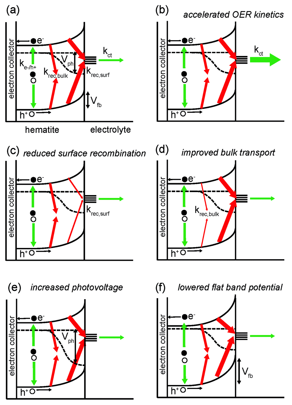 | ||
| Fig. 2 (a) Schematics of PEC processes in the bulk of hematite and at the hematite/electrolyte interface for potentials more anodic than the flat band potential Vfb. Green arrows indicate desirable processes: photon absorption and consequent electron–hole pair generation (at a rate ke−/h+) and charge transfer to the electrolyte (assumed to take place here from surface states) at a rate kct. Red arrows, instead, denote unwanted processes: charge recombination in the bulk (at a rate krec,bulk) and at the solid/liquid junction (at a rate krec,surf). The thickness of the arrows indicates the relative importance of the above mentioned processes in a typical hematite photoanode, resulting in highly anodic values of OER Vonset. Panels (b–f) illustrate how Vonset can be shifted towards more cathodic values by: (b) increasing kct, (c) reducing krec,surf, (d) reducing krec,bulk, (e) increasing Vph, and (f) lowering Vfb. | ||
In order to improve one (or more) of the aforementioned properties and thus to lower Vonset, several approaches have been tested experimentally, as summarized in Table 1. It is clear that there are recurring strategies in the field, such as: doping hematite, introducing overlayers on top of hematite, or other (oxide) layers between hematite and the electron collector/substrate. As one can expect, and as we will discuss in what follows, modifying hematite by one technique in order to modify one particular property often affects other characteristics of the electrode, not necessarily in a beneficial way and sometimes leading to a decrease in overall performance.
| Altered physical property | Experimental approach(es) | References |
|---|---|---|
| Increase kct | Overlayers | 129, 143, 146, 149–152 and 154 |
| Reduce krec,surf | Overlayers | 39, 41, 68 and 155–164 |
| Post-fabrication treatments | 165 | |
| Reduce krec,bulk | Doping | 41, 96 and 166–170 |
| Nanostructured substrates | 113 and 114 | |
| Extra layers between Fe2O3 and electron collector | 42 and 171–175 | |
| Increase Vph | Overlayers | 124 and 186 |
| Lower Vfb | Post-fabrication treatments | 87 |
| Modified fabrication | 189 |
Before we proceed to a more detailed description of the strategies outlined earlier, we mention that different methods are used in the literature to extract the value of Vonset from a PEC experiment. In particular, Vonset is often extracted from a j(V) plot as: (i) the potential at which the photocurrent density exceeds a certain defined value;129 or (ii) the potential at which the first derivative of the photocurrent density with respect to the potential, dj/dV, exceeds a certain defined value;130 or (iii) the potential at which the tangent to the j(V) curve in the region of maximum slope intersects the j(V) curve measured in the dark.131 All these definitions are somewhat arbitrary and may be more or less appropriate depending on the shape of the j(V) curves to be analyzed. For instance, using method (iii) can result in a situation where a curve with a steep slope will have a more anodic Vonset than the one with a flatter slope, although they may have the same Vonset according to other methods. Thus, the choice of method to define Vonset may affect the exact values extracted from the j(V) curves. Finally, the absolute Vonset value may also depend on some properties of the experimental setup, for instance the illumination intensity (on which Vph depends logarithmically before saturation) and spectral distribution. Therefore, when reviewing the recent progress in the topic, we will focus here on the variation of Vonset rather than on their absolute values.
Accelerating the OER kinetics
The most immediate attempts to improve the performance of hematite often consist in coupling it with an electrocatalyst characterized by a higher turnover frequency. The understanding of the OER has increased significantly over the last decade thanks to the combination of detailed electrochemical characterization132–134 with first-principles calculations135–137 (mostly based on the density functional theory, DFT). Together with the well-known high activity for OER (and HER) of Pt,138,139 ruthenium oxide (RuO2), iridium oxide (IrO2), Co and Ni based compounds have emerged as efficient catalysts.RuO2 and IrO2 are both very close to the top of the volcano plot with regard to the OER activity.137,140 While RuO2 has already been tested as an OER co-catalyst for overall water splitting on Ga1−xZxN1−xOx141 and for the HER on CuO2,142 its performance as a co-catalyst for the OER on hematite is still to be investigated. However, organometallic Ru-containing complexes have recently been tested on hematite. Chen et al.143 reported for instance a Vonset shift of about 300 mV for a hematite photoanode coated with a Ru(tpy)(pba)Cl Ru(II) complex.
IrO2 nanoparticles on a glassy carbon support achieve an OER current of 0.5 mA cm−2 at an overpotential of 0.25 V.144,145 Tilley et al.146 first attempted to couple IrO2 to a nanocauliflower structured hematite photoanode by electrophoretic deposition. While they observed a cathodic Vonset shift of 200 mV, cyclic voltammetry and chronoamperometry measurements indicated a decrease in photocurrent, caused by the detachment of IrO2 nanoparticles from the surface. The original performance could be restored by re-decorating the photoanode with additional nanoparticles. More recently, IrO2 films were deposited on top of hematite photoanodes by means of electrodeposition, using [Cp*Ir-(H2O)3](SO4) as the organometallic source of Ir.129 A stable, maximum Vonset shift of 300 mV was obtained for the optimized precursor concentration (Fig. 3a). EIS revealed that the capacitance associated with surface states peaks for potentials corresponding to the OER Vonset, indicating that the surface states are charged with holes and then discharged when the OER is initiated. Such behavior indicates that the OER takes place via surface states, for this system. Mott–Schottky analysis indicated that Vfb, and therefore the edge of the conduction band, remains unaffected by the addition of the IrO2 layer.
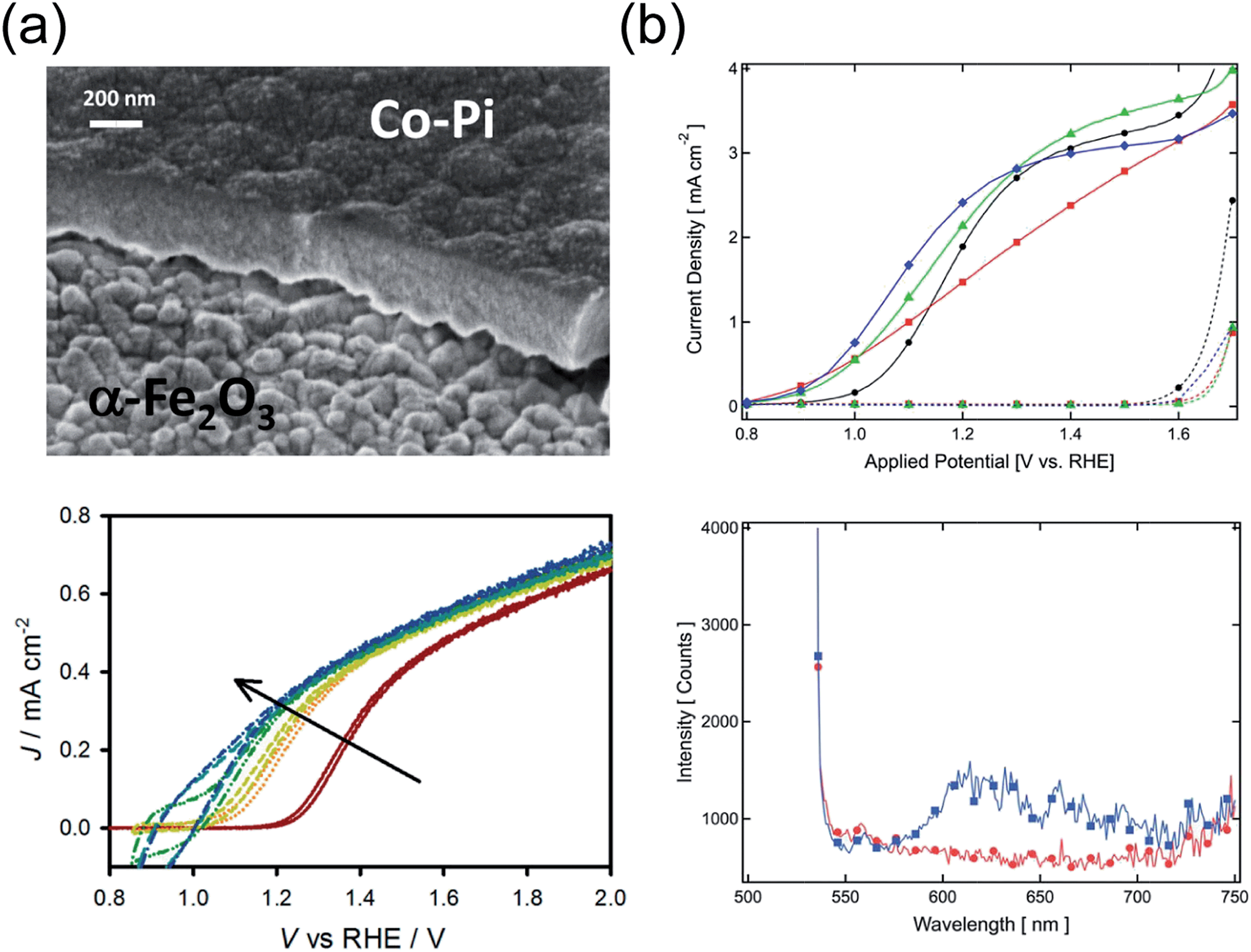
The (extreme) scarcity of both Ir and Ru poses questions on the scalability of PEC systems based on these compounds.2 Fortunately, other OER catalysts have emerged, mainly based on first row transition metals such as Co and Ni. For example, the so-called “Co–Pi” cluster, first developed in 2008, is capable of initiating the OER at 1.7 V vs. RHE in a neutral environment.147 Electrodeposition of Co–Pi films on top of hematite has been attempted, both in the dark and under illumination. After optimizing each of these two processes independently on the same dendritic photoanodes, Zhong et al.148 demonstrated a Vonset cathodic shift of 120 and 100 mV upon photoassisted and dark electrodeposition of Co–Pi, respectively. The slightly better performance of the former method was ascribed to the more uniform deposition of the catalyst on the hematite surface, instead of the preferential deposition on pinholes for the latter one.
However, the thickness of the catalyst after optimization may be such that light absorption in the catalyst itself might compete with absorption in hematite, leading to the need for illumination from the back-side of the photoanode and thus to device design constraints. This issue was tackled for instance by Riha et al.,149 who demonstrated a Vonset shift of 100 and 200 mV after coating planar and nanostructured hematite electrodes, respectively, with a Co-based sub-monolayer catalyst deposited by one cycle of atomic layer deposition (ALD) (Fig. 3b). The difference in Vonset was elucidated in terms of faster charge transfer from the surface states in modified photoanodes than from the surface states in bare electrodes, as indicated by the decreased surface state capacitance and the faster photocurrent transients observed for the coated electrodes. Moreover, XPS and XANES showed that the ALD coating consisted of 90% Co(OH)2 and 10% CO3O4 before PEC characterization, whereas a much higher CO3O4 content was found after the measurements in an alkaline environment.
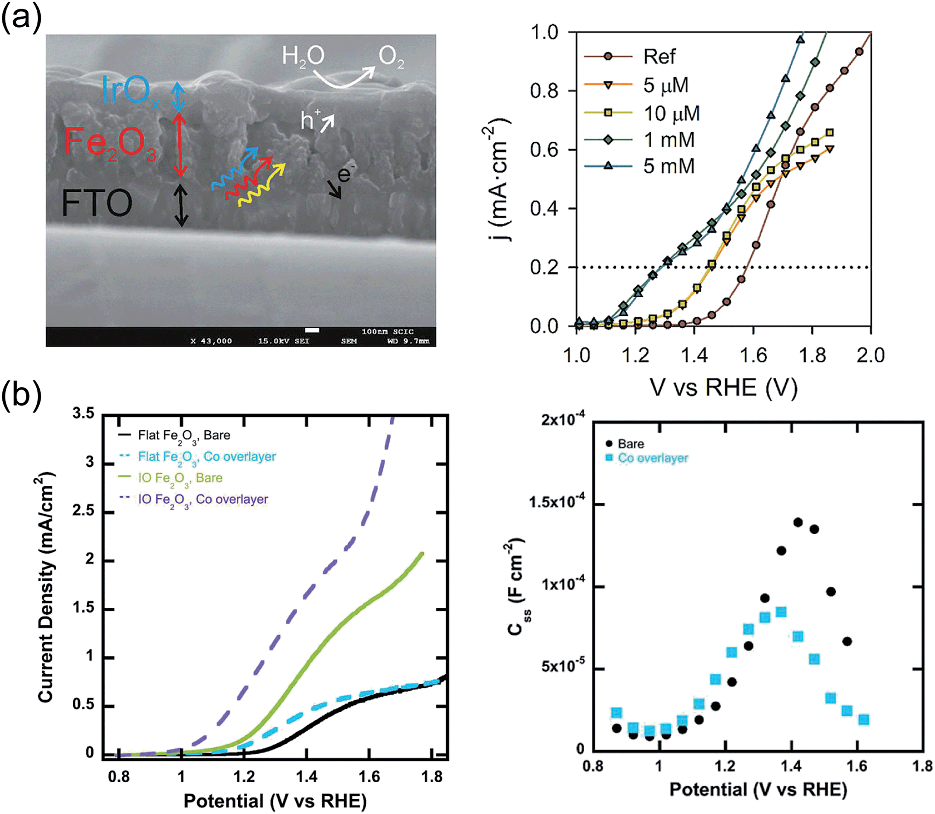 | ||
| Fig. 3 (a) Left: Cross-section SEM micrograph of the FTO/hematite/IrO2 catalyst layer. Right: j(V) characteristics of hematite films covered with layers of IrO2 with increasing thickness (right). Reproduced with permission from ref. 129. Copyright 2013 American Chemical Society. (b) Left: j(V) curves for hematite films deposited on inverted opal scaffolds and covered with a Co oxide layer (left). Right: Surface states charge extracted from EIS under illumination on bare hematite and hematite after adsorption of Co oxide layer. Reproduced with permission from ref. 149. Copyright 2013 American Chemical Society. | ||
Ni hydroxides and oxides have also shown interesting catalytic activity towards OER. Nonetheless, a mechanistic study by Li et al.150 indicated that, while photoanodes based on hematite nanowires decorated with Ni(OH)2 by successive dipping into Ni(NO3)2 and NaOH solutions showed larger photocurrent during cyclic voltammetry, the steady-state photocurrent measured by chronoamperometry was smaller than in reference electrodes. The larger photocurrent response in the cyclic voltammetry experiment was understood to generate from the slow Ni2+–Ni3+ oxidation, which eventually depletes the Ni(OH)2. While cyclic voltammetry is certainly a simple, fast and often information-rich technique for preliminary evaluation of the OER photoactivity, this study shows that it is crucial to measure the steady-state photocurrent of the photoanodes (and preferably to quantify the reaction products by means of gas chromatography or mass spectrometry) in order to confirm the true photoactivity of the system.151 More recently, Young and Hamann152 showed a cathodic shift of Vonset of about 300 mV from steady state photocurrent measurements of hematite films covered by NiO by ALD. Such a result was obtained upon following a procedure developed by Trotochaud et al.,153 in which the NiO-coated photoanodes were held at a constant potential of 1.42 vs. RHE under illumination for 3 hours. This conditioning process was determined to induce a structural change from the cubic NiO to an ion-permeable hydroxide/oxyhydroxide structure based on Ni(OH)2, which was identified then as the active OER catalyst phase.
Finally, it is worth mentioning that a high activity of electrocatalysts in the dark does not always translate into improved performance when such catalysts are coupled to photoactive semiconductors. This concept was elegantly illustrated by Yang et al.154 in the case of MnOx/hematite. While MnOx showed indeed higher OER current in the dark than hematite (both deposited in the form of thin films by ALD), addition of MnOx onto hematite suppressed the photocurrent almost entirely. It was then hypothesized that introducing MnOx results in Fermi level pinning, and thus in a smaller Vph. Indeed, open circuit results confirmed that Vph decreased from about 200 mV to 5 mV or less for the composite electrodes, indicating a clearly reduced oxidative power for holes. This result exemplifies the possibility of affecting more than one property of the photoanode by, for instance, the introduction of an additional layer.
Reducing surface recombination
Recombination of holes with electrons at the surface suppresses the photocurrent in most hematite photoanodes for moderately anodic potentials. Several attempts to alleviate this issue relied on depositing some coating (overlayer) on hematite, in a similar fashion to coupling hematite to electrocatalysts. A simple yet beneficial treatment consists in surface adsorption of Co2+ ions, as first attempted on hematite by Kay et al.41 Treating the surface of a nanocauliflower electrode with a 10 mM Co(NO3)2 solution results in a Vonset shift of 80 mV, at an estimated coating thickness of just a monolayer. A very similar effect was obtained by performing the same procedure on a hematite photoanode fabricated by dip coating.155 Although these results were first believed to originate from accelerated charge transfer kinetics, later studies have elucidated that the role of the Co2+ ion layer (sometimes indicated as CoOx) is rather to reduce electron–hole recombination at the surface. Transient photocurrent and transient photovoltage measurements performed on the same previously mentioned type of nanocauliflower photoelectrode, before and after Co2+ absorption, revealed reduced accumulated charge at the surface of the treated electrodes, as well as increased transient photovoltage.156 These observations point at a reduced surface recombination rate krec,surf, and not at an increased kct. Miao et al.157 drew similar conclusions on the 100 mV Vonset shift observed on their hydrothermally grown, Ti-doped microstructured hematite nanoparticle films, based on results from EIS measurements.While the addition of Co–Pi layers is of proven benefit to the PEC performance of hematite, the exact mechanism of such improvement has not yet been unambiguously determined.158 Klahr et al.39 investigated the effect of Co–Pi on the photoelectrochemistry of flat hematite films grown by ALD. Transient photocurrents (Fig. 4a) indicate an increasing charging current with increasing Co–Pi thickness, which are attributed to the oxidation of Co3+ to Co4+ within the Co–Pi layer by hematite valence band holes. The EIS spectra were modeled by introducing a capacitance and charge transfer resistance associated with the Co–Pi, from which it was concluded that the latter was a fast hole-scavenger. Furthermore, MS analysis suggests that the band bending in the photoelectrode is essentially independent of the Co–Pi. In view of these results, the Co–Pi was inferred to extract photogenerated holes from hematite, thus reducing krec,surf. The same conclusion was drawn by Shi et al.,159 who also observed a Vonset shift of about 220 mV upon light assisted electrodeposition of Co–Pi on hematite deposited on top of an inverse opal structured substrate.
On the other hand, Barroso and co-workers160 have suggested a different scenario, based on their measurements on mesostructured hematite photoanodes (fabricated by APCVD or by ultrasonic spray pyrolysis) modified with Co–Pi overlayers. Transient optical absorption experiments indicated that the presence of Co–Pi induces a strong elongation of a feature centered at 700 nm, which has been assigned previously to holes generated within bulk hematite. Such transient hole decay is strongly dependent on the applied bias, and correlates well with the cathodic Vonset observed during cyclic voltammetry and chronoamperometry. Based on these data, the authors proposed that the Co–Pi traps electrons from hematite, and not holes, thus increasing the band bending within hematite itself. In this picture, therefore, the resulting beneficial effect would be an increased charge transport in hematite thanks to reduced bulk recombination. Accordingly, there would be no transfer of holes from hematite to the Co–Pi, and the OER would still take place at the surface of hematite. These different mechanistic interpretations of the role played by Co–Pi have eventually been reconciled by Gamelin and coworkers,161 who performed microscopic, electrochemical, and spectroscopic measurements on mesostructured Co–Pi/hematite composite photoanodes that revealed different beneficial effects of the Co–Pi layer when its thickness is changed.
Co-based coatings are not the only overlayers that have proven effective in reducing krec,surf. le Formal et al.68 reported a Vonset shift of 80 mV upon a one-cycle ALD coating of nanostructured hematite photoanodes with Al2O3. Thicknesses of up to 13 cycles of Al2O3 were tested, showing a similar beneficial effect in terms of Vonset shift. However, the coatings dissolved after 1 h chronoamperometry under 1 sun illumination at 1.05 V vs. RHE. Transient photocurrent measurements and EIS indicated a lower surface recombination rate while the position of the band edges in hematite was unaffected. Finally, photoluminescence at wavelengths between 600 and 700 nm was observed in Al2O3-coated photoelectrodes, pointing at a passivating effect of the overlayer on the surface states (the OER was found here to take place via direct transfer of holes from the valence band) (Fig. 4b).
 | ||
| Fig. 4 (a) Cross-section SEM micrograph of hematite/Co–Pi overlayer (top), j(V) curves of hematite covered with Co–Pi layers with increasing thickness (bottom). Reproduced with permission from ref. 39. Copyright 2012 American Chemical Society. (b) Top: j(V) characteristics of hematite photoanodes fabricated via APCVD before ALD of 1 cycle of Al2O3 overlayer (black circles), after ALD (red squares), after annealing for 20 min at 300 °C (green triangles) and after annealing for 20 min at 400 °C (blue diamonds). Bottom: Photoluminescence emission spectra from APCVD hematite before (red circles) and after 3 ALD cycles of Al2O3, on its surface (blue squares). Reproduced with permission from ref. 68. Copyright 2011 The Royal Society of Chemistry. | ||
Spurred by these observations, Hisatomi and coworkers162 undertook a systematic screening of the effect of 13-group oxide overlayers on the photoelectrochemistry of hematite ultra-thin films fabricated by USP. The coatings, consisting of Al2O3, Ga2O3, or In2O3, were prepared by chemical bath deposition based on urea hydrolysis. The highest Vonset shift of 200 mV was obtained with a Ga2O3 coating after calcination at 500 °C. The after-deposition thermal treatment also helped preventing dissolution of the overlayer for about one day. The superior performance of Ga2O3 as compared to the other coatings was rationalized in terms of the ability of Ga2O3 (which has the smallest lattice mismatch with hematite) to release lattice strain of the thin hematite layers.
Besides 13-group oxide overlayers, Xi and coworkers163 demonstrated a 170 mV cathodic Vonset shift on hematite films fabricated by spray pyrolysis upon coating with a ZnO layer deposited by spin-coating a zinc acetate solution in ethanol and subsequent calcination at 400 °C. An optimal number of 3 cycles was found, resulting in a ZnO thickness of a few nm as estimated by XPS. The beneficial effect of the surface treatment in terms of suppressing surface recombination was assessed by extracting the ideality factor from current–potential measurements performed in the dark under forward bias. A shift of Vfb towards lower values of about 35 mV was determined from MS plots, which may also have partly contributed to the observed Vonset shift. The same group modified a route to incorporate a thin coating of FexSn1−xO4 on the surface of hydrothermally grown FeOOH nanowires.164 The thickness of the amorphous FexSn1−xO4 was determined to be 1–2 nm by high resolution TEM imaging. Chopped chronoamperometry and ideality factor measurements in the dark both supported the claim that FexSn1−xO4 improves the delivery of holes to the electrolyte by decreasing krec,surf.
Finally, further post-fabrication treatments have proven to decrease krec,surf. For instance, Zhang et al.165 demonstrated a Vonset shift of about 200 mV for hematite films fabricated by USP, after prolonged chronoamperometry in a saturated NaCl electrolyte under illumination of intensity of ca. 400 mW cm−2. Dissolution of the outermost layers of the hematite films during this treatment was inferred from inductively coupled plasma mass spectrometry analysis. Photocurrent transients were found to be less pronounced for treated electrodes, which, coupled with an increase in the photoluminescence signal centered around 610 nm, indicated a beneficial effect of the treatment on the hole transfer efficiency across the hematite/electrolyte interface.
Improving carrier transport in bulk
The most common strategy to alleviate the issue of bulk recombination consists in doping hematite. Perhaps the most emphasized result of incorporating foreign atoms is the enhanced maximum photocurrent jmax. Nevertheless, a Vonset shift is also often observed, due to the fact that for moderately anodic potentials not only ηct, but also ηtr is far from unity. A beneficial effect of doping on Vonset is mentioned in some reports, and can originate from the enhanced conductivity thanks to the increase in charge donors, from the improved morphology of hematite, or from both.For instance, Cao et al.166 showed a Vonset shift of about 100 mV on hematite films grown via hydrothermal reaction upon Ti doping during fabrication. While the doped samples did not show any appreciable difference from reference electrodes in terms of surface structure, morphology and radiative recombination by photoluminescence, a clear increase in the donor concentration was determined from doping with Ti4+, which accounted for the improved PEC performance. Cong and co-workers167 reported a beneficial synergistic effect of Al and Ta co-doping of hematite films grown by drop casting and subsequent annealing. While Al3+ incorporation in hematite does not increase the charge carrier density, its smaller ionic radius as compared to Fe3+ was shown to facilitate charge hopping through the semiconductor. Ta5+ ions, instead, enhance the conductivity in a similar fashion to Ti4+ and Si4+ dopants. Optimized 0.25% Ta/10% Al co-doped hematite films showed a Vonset more than 200 mV more cathodic than 10% Al only doped electrodes, even though Vfb was determined to be higher by 50 mV in the former case. EIS under illumination revealed a drastically reduced resistance for the co-doped electrodes, corroborating the hypothesis of reduced bulk recombination.
Coupling of hematite photoanodes with carbon nanotubes has also been explored recently. Kim et al.168 found an anodic Vonset shift of about 50 mV on a multi-walled carbon nanotubes/hematite composite electrode, where the hematite films were fabricated by calcination of Fe nanoparticle films. On the other hand, they observed a beneficial effect of the nanotubes on jmax, which increased by a factor of about 3 thanks to the enhanced bulk conductivity as confirmed by EIS characterization. Liu and coworkers,96 instead, found a cathodic Vonset shift of 140 mV upon functionalization of Ti-doped electrodeposited hematite films with carbon nanotubes, which were dispersed in the electrodeposition solution prior to fabrication. A combination of transient photocurrent and EIS measurements was employed to support the hypothesis that the carbon nanotubes work as an efficient electron sink, thus reducing electron–hole recombination in the bulk.
Doping of hematite can also be accomplished as post-fabrication treatment, as demonstrated by Franking and coworkers,169 who developed a method to dope hematite nanowire films by depositing a doping precursor solution (Ti or Zr) with subsequent annealing at 650–700 °C. A 50 mV Vonset shift was found after 30 minutes annealing of the films after modification with the Ti-containing precursor. The enhanced PEC performance was attributed to the one order of magnitude increase in charge carrier density, as determined by MS analysis. Interaction of the dopant atoms with surface states in hematite, however, was inferred from EIS under illumination, and could also play a role in the superior performance of the treated photoanodes.
The influence of doping on the morphology of hematite is perhaps best exemplified by the results reported by Kay et al.41 in 2006, which demonstrated for the first time dendritic, cauliflower-like nanostructured hematite with a strong preferential orientation of the [110] axis vertical to the substrate induced by Si4+ doping. Photoanodes fabricated through the same APCVD technique are still the benchmark for the OER on hematite. More recently, Lee and coworkers showed that Si doping of hematite nanotubes resulted in more pronounced nanotubular morphology than for unintentionally doped samples.170 Although XRD analysis did not show a drastic improvement in crystallinity, the increased surface area of the Si doped electrodes resulted in an appreciable Vonset shift of around 160 mV.
Depositing hematite on nanostructured templates has proven to be an effective means to increase ηtr, and therefore improving the PEC performance at low applied bias. Riha et al.113 employed a simple fabrication protocol to deposit hematite by ALD on top of a porous inverse opal scaffold substrate. These nanostructured electrodes showed a 200 mV Vonset shift as well as a 3-fold increase of jmax at 1.53 vs. RHE as compared to flat ITO/hematite films. Along the same line, Lin and coworkers104 realized nanostructured hematite photoanodes by conformal ALD coating of high conductivity, highly crystalline TiSi2 nanonets constituting of belts about 1–2 μm long and around 15 nm in diameter (Fig. 5a–c). These nanonets served as both a substrate support and an electron collector, thus providing an interesting alternative to transparent conductive oxides. The bulk recombination was dramatically reduced as compared to planar film geometry, leading to a cathodic Vonset shift of around 150 mV as well as an enhancement of jmax by a factor of five. While in both these reports ALD is used to cover the nanostructured substrate in a conformal way with low defect concentration hematite, this approach may be extended by doping the hematite and by depositing it via more easily scalable techniques.
A common denominator in the poor ηtr observed for many hematite based photoanodes is charge recombination at the solid/solid interface between hematite and the electron collection layer. This issue can be alleviated by introducing an additional layer between the charge collector and the hematite, which has a proper conduction band edge position in order to mitigate the recombination at the back of the electrode. Hisatomi and coworkers171 first investigated the effect of ALD fabricated Nb2O5 and TiO2 underlayers on the PEC properties of ultra-thin hematite deposited by USP (Fig. 5d). When deposited directly on FTO, hematite films of thickness lower than 20 nm showed negligible photocurrent, while they started the OER at around 1.1 V vs. RHE and reached jmax between 0.6 and 0.7 mA cm−2 upon introduction of a Nb2O5 or TiO2 underlayer. The photocurrent decreased with increasing thickness of the TiO2 underlayer, which was explained by the need for electrons to tunnel through the underlayer to reach the FTO due to the high offset of 0.6 eV between the conduction band edges of TiO2 and hematite. On the other hand, thanks to the lower offset in the case of Nb2O5/hematite (only 0.2 eV), the photocurrent increased with increasing Nb2O5 thickness (at constant Vonset), stabilizing at a thickness of 1.5 nm. The most convincing evidence that the performance improvement originated from the suppression of back injection of electrons came from the drastic reduction in cathodic dark current measured in the presence of the fast Fe(II)(CN)64−/Fe(III)(CN)63− redox couple. A very similar trend was observed by Wang et al.172 for TiO2 underlayers between FTO and comparatively thicker (100 nm) hematite films deposited by the same USP. In this case the underlayer was obtained by a layer-by-layer exfoliation from titanium oxide nanosheets followed by calcination. The authors also found an optimal thickness of the underlayer, given by 2 nanosheet deposition cycles, corresponding to 1.46 nm in excellent agreement with the previous report.
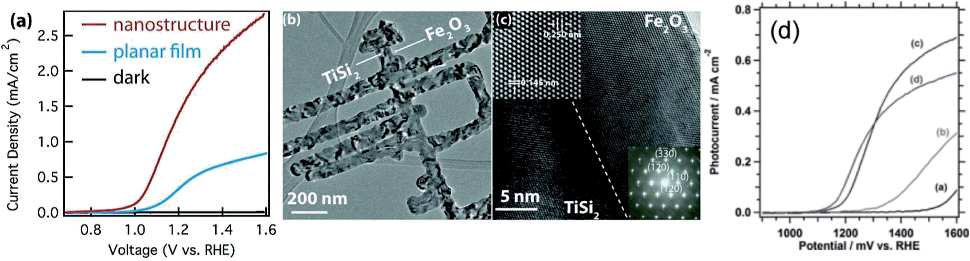 | ||
| Fig. 5 (a–c) j(V) plots of hematite deposited by ALD on a TiSi2 nanonet substrate and of a planar hematite film; low-magnification TEM image of a typical TiSi2/hematite core/shell nanostructrure; and high-resolution TEM data including lattice-fringe-resolved HRTEM image and electron diffraction pattern of hematite. Reproduced with permission from ref. 104. Copyright 2011 American Chemical Society. (d): j(V) curves of 16–19 nm thick hematite deposited by USP on FTO substrates modified with different underlayers: (a) no underlayer, (b) SiOx monolayer by TEOS spraying, (c) 2 nm thick ALD Nb2O5, and (d) 1 nm thick ALD TiO2. Reproduced with permission from ref. 171. Copyright 2012 John Wiley & Sons. | ||
A variety of further underlayers have been tested recently with similar promising results. Meng and coworkers173 prepared composite reduced graphene oxide/hematite photoanodes. The superior performance of the composite photoanodes was established by cyclic voltammetry, transient photocurrent and TAS measurements, showing a Vonset shift of about 200 mV compared to bare hematite samples. Yang and coworkers174 demonstrated a cathodic Vonset shift of almost 100 mV by introducing an unintentionally doped hematite underlayer between the FTO substrate and Ti-doped nanowire hematite films. The beneficial effect was explained in terms of suppression of back injection of electrons thanks to the lower conductivity of the unintentionally doped underlayer as compared to the Ti-doped nanowires.
The introduction of other oxide layers between the charge collector and hematite often provides a template for growth of hematite of higher quality in terms of reduced growth stress, improved crystallinity or improved morphology. le Formal and coworkers175 showed that pretreating FTO substrates with tetraethoxysilicate (TEOS) prior to deposition of hematite by USP resulted in a Vonset shift of 70 mV for 23 nm thick hematite films. Detailed physical characterization of these ultra-thin films revealed that the pretreatment resulted in the formation of a monolayer of SiOx on the substrate. The subsequently deposited hematite films showed increased crystallinity and reduced defects acting as trapping states, as determined by XRD and transient photocurrent measurements. It was suggested that such differences arise from different film formation processes: a Frank–van der Merwe growth (i.e. full layer covering the substrate) and a Volmer–Weber growth mode (i.e. film formation by islands) on SiOx modified and bare FTO substrate respectively. Similar results were obtained by Hisatomi et al.42 using a Ga2O3 underlayer deposited by ALD prior to deposition of ultra-thin hematite films by USP. After optimization of the thickness of the underlayer, a Vonset shift of 200 mV was demonstrated. Based on investigation of the morphology and crystallinity by SEM and XRD respectively, it was asserted that the underlayer works as an isostructural template for the hematite growth.
Finally, several further studies have demonstrated the beneficial effect of improved quality of hematite on the bulk recombination.85,105,173–185 The schemes explored to obtain such performance improvement include: coating with suitable overlayers, co-sputtering of other oxides with hematite to obtain solid oxide solutions, tuning fabrication parameters or optimizing the post-fabrication annealing conditions.
Increasing photovoltage
As described in the Introduction, the difference between quasi-Fermi levels for electrons and holes (EF,n and EF,p respectively) determines the photovoltage Vph in the semiconductor. The latter can in principle approach the optical bandgap, however this is far from being the case for hematite in practice. The magnitude of Vph is normally determined by measuring the difference between open circuit potential, OCP (i.e. when no net current flow is present at the semiconductor/electrolyte interface) in the dark and under illumination. At equilibrium in the dark, the OCP reports on the position of the Fermi level, i.e. EF,n = EF,p = EF. Under illumination, the equilibrium between the photoelectrode and electrolyte is instead maintained by EF,p. Therefore, the difference between the OCP measured in the two situations corresponds to the Vph. The latter is often 0.2–0.3 eV for hematite,124 highlighting the potential room for improvement. However, it was not until very recently that strategies to increase Vph, and thus the driving force of holes towards the OER, were demonstrated.In the first case, Du et al.124 reported a Vonset shift as high as 380 mV upon decorating hematite films with an amorphous NiFeOx layer, prepared by photochemical metal–organic deposition (Fig. 6a). While NiFeOx was recently identified as an efficient OER catalyst in the dark, its beneficial effect on the photoelectrochemistry of hematite was rationalized as originating from an increase of Vph rather than an acceleration of kct. In fact, while the open circuit potential under illumination was practically unmodified by the presence of NiFeOx, the open circuit potential in the dark shifted from 0.85 V in the case of bare hematite to 1.23 V after modification. Such a difference of 380 mV arises from removal of the surface states pinning at the hematite/electrolyte junction, and accounts for the observed Vonset shift.
In the second case, 5 nm thick, p-type Mg-doped hematite was grown on n-type (due to oxygen vacancies) hematite films.186 TEM imaging revealed that the growth of p-type hematite does not introduce additional structural defects. Cyclic voltammetry indicated a 200 mV shift of Vonset upon deposition of the p-type hematite coating (Fig. 6b). The presence of the additional in-built field leading to the increase in Vph was confirmed by EIS performed in the dark as well as by transient Vph measurements, which demonstrated that the buried p–n junction acts as a favorable charge recombination center when light is switched off. Moreover, changes in optical absorption and in film thickness were ruled out as possible parameters influencing the difference in PEC performance, while a MgO coating on hematite control films did not show any Vonset shift thus excluding the possibility that the p-type coating reduces charge recombination at the surface.
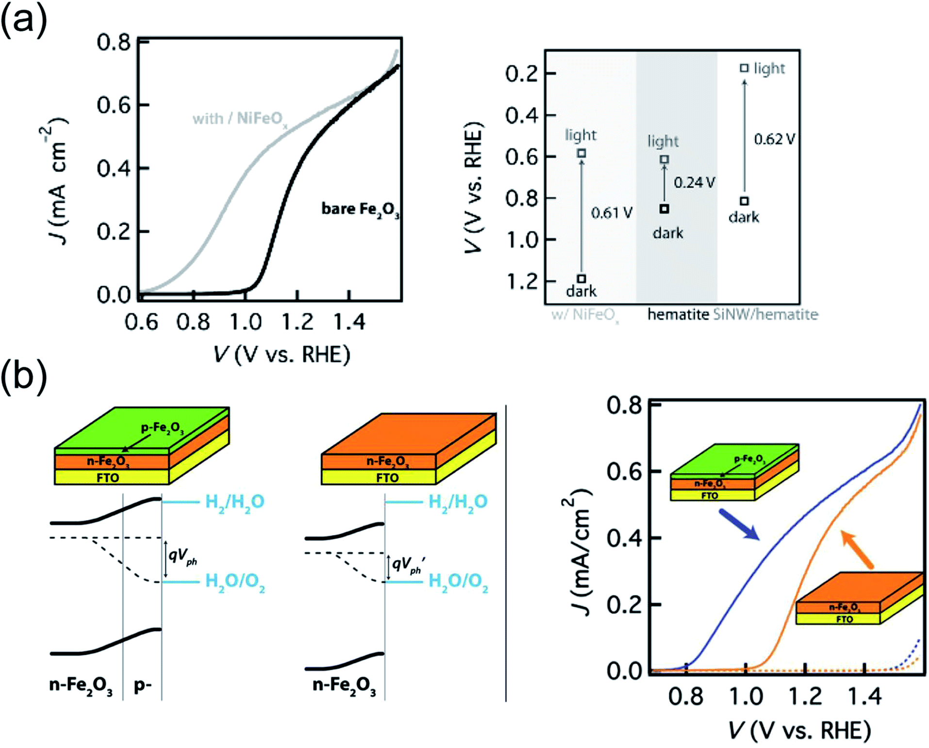 | ||
| Fig. 6 (a) Left: j(V) plots of bare hematite film deposited by ALD (black) and after surface modification of hematite with NiFeOx (grey). Right: Measured Vph generated by hematite decorated with NiFeOx, bare hematite and hematite on Si nanowires (left, middle and right in the graph respectively). Reproduced with permission from ref. 124. Copyright 2013 The German Chemical Society. (b) Left: Energy band diagrams of unintentionally doped n-type hematite with a p-type hematite coating as compared with that of a bare n-type hematite. The presence of the p-type layer creates a built-in field that does not depend on the properties of the semiconductor/electrolyte interface, allowing an increased Vph. Right: j(V) curves of n-type hematite with and without p-type coating (same total thickness of 25 nm). Reproduced with permission from ref. 186. Copyright 2012 American Chemical Society. | ||
Shifting the flat band potential
Another interesting, yet largely unexplored strategy to lower Vonset consists in lowering Vfb in hematite. If this goal is accomplished, the potential at which the bands in the semiconductor start bending upwards, thus driving holes toward the semiconductor/electrolyte interface, is also lowered. The same effect can be explained in that, for a given value of applied potential, the width of the depletion layer WSC is increased since WSC typically scales with (V − Vfb)0.5. Lowering Vfb is therefore desirable since it would lead to a lowering of Vonset as well, provided that the other PEC properties of the system remain unmodified. A modification of Vfb resulting in enhanced TiO2 based photocatalysis has been demonstrated, for instance by tuning the level of oxygen vacancies.187,188 Recently, a similar effect has also been reported for hematite-based PEC devices.87,163,189Part of the Vonset shift observed by Xi et al.163 upon modification of hematite with a ZnO overlayer was explained by a lowering of Vfb of 35 mV. A more substantial Vfb shift was demonstrated by Hu and coworkers87 on a system consisting of a Ti-doped hematite film fabricated by electrodeposition, which was treated with a CoF3 solution (Fig. 7a). XPS depth analysis indicated that the surface of the Ti-doped samples is enriched with Ti relative to the bulk of the film, which facilitates the grafting of F− ions to the surface due to the more favorable Gibbs free energy of TiFe3 formation as compared to FeF3. Photoelectrodes treated with the CoF3 solution showed a cathodic Vonset shift of 200 mV as compared to untreated samples. A Vfb shift of 170 mV was determined from MS analysis, which accounted for the beneficial effect on Vonset.
It is also possible to lower Vfb in hematite without additional layers or other post-fabrication treatments.189 A lowering of Vfb of 200 mV on polycrystalline ultra-thin hematite films was achieved by prolonging the oxidation process during which the Fe films were converted into hematite (Fig. 7b). An excellent agreement between the shift of Vfb extracted from MS analysis and that of Vonset observed during photocurrent measurements was found, while the plateau photocurrent only increased by about 10%. Optical absorption, surface composition, density of surface states and roughness were all unaffected by the prolonged oxidation. TEM analysis, instead, revealed an increase in grain size (and thus decreasing grain boundary density) for increasing oxidation time that correlated qualitatively with the observed Vfb, in terms of reduced potential losses at boundaries within the hematite.
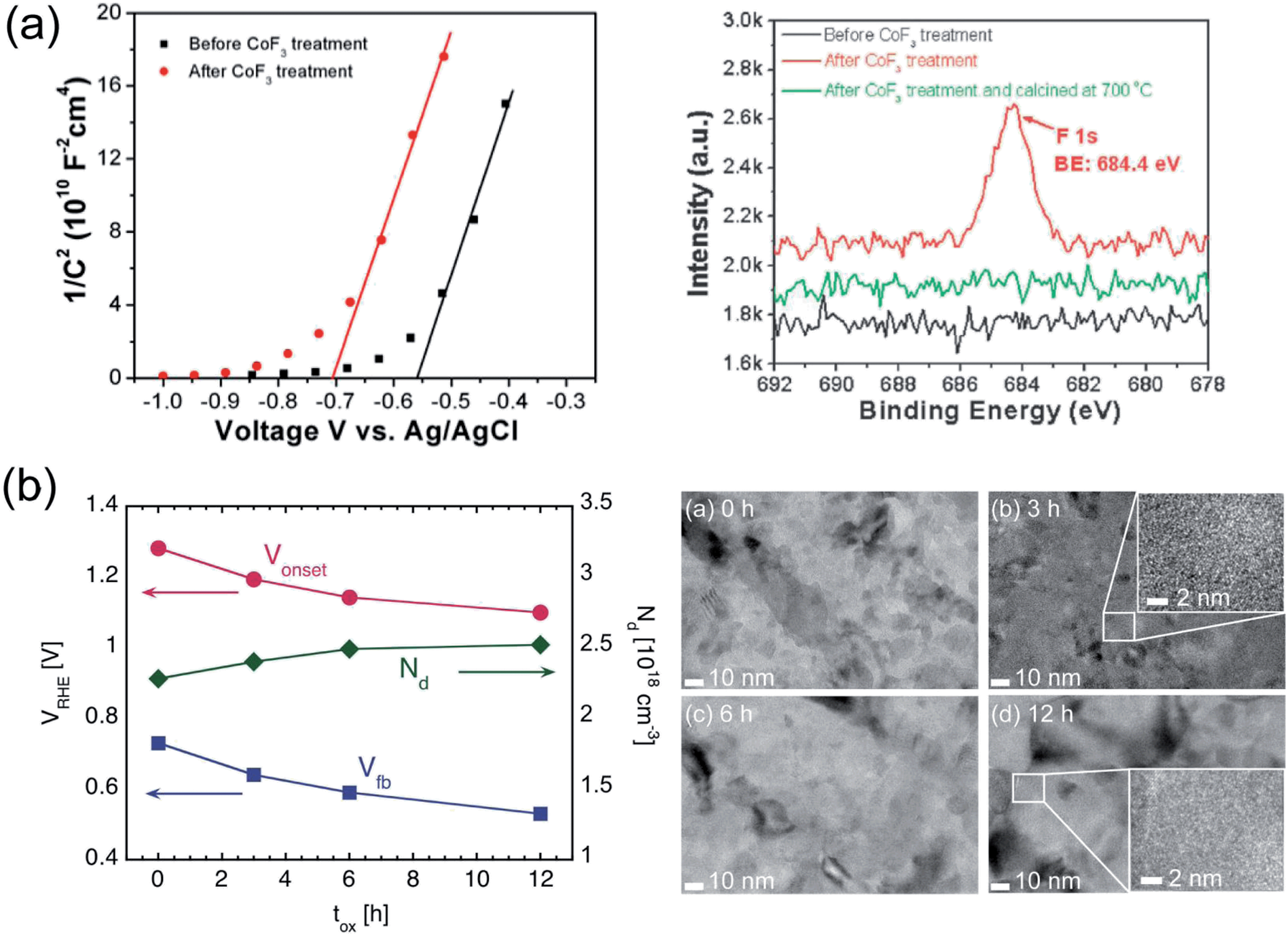 | ||
| Fig. 7 (a) Left: MS plots for electrodeposited hematite films before and after treatment in solution containing CoF3. Right: F 1s high-resolution XPS spectra of Ti-doped hematite film, Ti-doped hematite film after CoF3 aqueous solution treatment without and with high temperature calcination. Reproduced with permission from ref. 87. Copyright 2009 The Royal Society of Chemistry. (b) Left: Vonset and Vfb of ultrathin hematite films fabricated by thermal oxidation of Fe, as a function of oxidation time. The majority charge carrier concentration ND is also plotted. Right: TEM images of hematite films held at 350 °C during thermal conversion for 0, 3, 6 and 12 h. High magnification insets are also present for 3 and 12 h samples. From ref. 189. | ||
Conclusions
Decades of research on the PEC properties of hematite have identified a number of specific limitations that have prevented us so far from achieving the theoretical maximum STH conversion efficiency of this material. Nevertheless, the favorable characteristics of hematite in terms of bandgap energy, exceptional stability and availability make it one of the most promising candidates for solar energy storage. Here we have analyzed in detail a major issue that needs to be solved in order to make hematite suitable for large-scale applications, namely the highly anodic electrochemical potential required to initiate the OER. We now understand this to be the result of a combination of several factors and properties, both of hematite and of the hematite/electrolyte interface: a slow OER kinetics, often much slower than charge recombination at the hematite/electrolyte interface; bulk losses arising from charge recombination within hematite; a small Vph compared to the optical bandgap, resulting in a low oxidative power of holes; and an often high value of Vfb.We have summarized the recent advancements in lowering Vonset, which in most cases focus on improving one of the aforementioned processes/properties (OER kinetics, surface recombination, bulk recombination, photovoltage and flat band potential) at the time. Several experimental strategies have proven effective, and some of them demonstrated remarkable improvements, with measured Vonset shifts of up to 0.4 V as compared to reference samples without modifications. Moreover, many of these approaches are (in principle) compatible with one another, for instance doping of hematite with underlayers and/or (catalyst) overlayers. Indeed, hematite based composite photoanodes that incorporate different modifications have been successfully fabricated. Nonetheless, the performance of such modified photoelectrodes is still quite far from what can be achieved using hematite, with an ideal performance of Vonset = Vfb = 0.4–0.5 V and a jmax = 12 mA cm−2 reached within 0.1 V of Vonset. A further motivation to push the performance of hematite consists in that reaching jmax at 0.7 V or lower potential would allow for using one single-junction Si-based PV device in series with the photoanode, to provide all the necessary bias to run the OER.
The following considerations can be made to rationalize the performance gap in hematite. First, the majority of the studies presented here are characterized by the use of model photoelectrodes, and in general by photoelectrodes whose performance is far from state-of-the-art. While these studies are undoubtedly important as proof-of-principle for new avenues for improvement and as platforms for increasing material understanding, it is indeed questionable whether the beneficial effect would be translated quantitatively to state-of-the-art photoelectrodes. Second, a few modifications of hematite have been shown to affect more than one property of the system, and not always in a beneficial way. In some cases, the overall performance of the photoanodes was even worsened as compared to unmodified samples. Third (and in relation to the previous point), when attempting to combine different modification strategies, the total Vonset shift is likely not given by the sum of the shifts seen for each modification alone, or in other words saturation of the performance improvement can be expected.
Clearly, there is plenty of room to improve both the kinetics of the OER and the energetics of the hematite/electrolyte junction. Moreover, the requirement of cheap and scalable fabrication calls for the use of deposition techniques yielding films characterized by significantly poorer quality (crystallinity, density of defects and so on) than for instance single crystal films, which calls for improving the properties of these photoelectrodes with (some of) the modifications discussed here. It is safe to assume that several of these approaches need to be combined in order to reach the goals described above, i.e. Vonset = Vfb = 0.4–0.5 V and a jmax = 12 mA cm−2 reached within 0.1 V of Vonset.
Doping (by foreign atoms or by tuning the amount of oxygen vacancies) is required to enhance electron conductivity, while the presence of an extra layer between hematite and the electron collector is the key to reduce the back-injection of electrons into hematite. These two strategies combined carry the promise of solving the issue of internal charge recombination. Furthermore, the addition of overlayers is paramount to accelerate the notoriously slow OER kinetics on hematite, as well as to increase the photovoltage sustained by the electrode. The question remains, however, whether these modifications are compatible with one another in practice: for instance, when some of them require heat treatment at temperatures that cannot be sustained by certain catalysts. Nevertheless, besides the remarkable advancements in hematite based water splitting over the last decade, the massive effort summarized here is crucial since it has enabled the PEC community to deepen the understanding of the properties of hematite tremendously. We consider this to be a key ingredient in designing photoanodes that will take advantage of the full potential of hematite.
Acknowledgements
B. I. and A. H. thank the Swedish Research Council, Formas (project numbers 219-2011-959 and 229-2009-772) and the Chalmers Area of Advance Material and Energy for financial support. B. W. thanks Formas (project number 219-2011-959) for financial support. I. Z. acknowledges support from the Swedish Pension Agency.References
- BP Statistical Review of World Energy, 2011, http://www.bp.com/en/global/corporate/about-bp/energy-economics/statistical-review-of-world-energy.html Search PubMed.
- P. C. K. Vesborg and T. F. Jaramillo, RSC Adv., 2012, 2, 7933 RSC.
- N. S. Lewis and D. G. Nocera, Proc. Natl. Acad. Sci. U. S. A., 2006, 103, 15729–15735 CrossRef CAS PubMed.
- N. Armaroli and V. Balzani, Angew. Chem., Int. Ed. Engl., 2007, 46, 52–66 CrossRef CAS PubMed.
- R. E. Smalley, MRS Bull., 2011, 30, 412–417 CrossRef.
- K. Rajeshwar, R. McConnell, K. Harrison and S. Licht, in Solar Hydrogen Generation – toward a Renewable Energy Future, Springer, New York, 2008 Search PubMed.
- J. Barber, Philos. Trans. R. Soc., A, 2007, 365, 1007–1023 CrossRef CAS PubMed.
- J. Turner, G. Sverdrup, M. K. Mann, P.-C. Maness, B. Kroposki, M. Ghirardi, R. J. Evans and D. Blake, Int. J. Energy Res., 2008, 32, 379–407 CrossRef CAS PubMed.
- D. Gust, T. A. Moore and A. L. Moore, Faraday Discuss., 2012, 155, 9 RSC.
- C. A. Grimes, O. K. Varghese and S. Ranjan, Light, Water, Hydrogen, Springer, 2008 Search PubMed.
- Ed. R. van de Krol and M. Grätzel, Photoelectrochemical Hydrogen Production, Springer, US, Boston, MA, 2012, vol. 102 Search PubMed.
- P. J. Boddy, J. Electrochem. Soc., 1968, 115, 199 CrossRef CAS PubMed.
- A. Fujishima and K. Honda, Nature, 1972, 238, 37–38 CrossRef CAS PubMed.
- M. Grätzel, Nature, 2001, 414, 338–344 CrossRef PubMed.
- F. E. Osterloh, Chem. Mater., 2008, 20, 35–54 CrossRef CAS.
- M. Woodhouse and B. A. Parkinson, Chem. Soc. Rev., 2009, 38, 197–210 RSC.
- J. Greeley, T. F. Jaramillo, J. Bonde, I. B. Chorkendorff and J. K. Nørskov, Nat. Mater., 2006, 5, 909–913 CrossRef CAS PubMed.
- A. Walsh, S.-H. Wei, Y. Yan, M. Al-Jassim, J. Turner, M. Woodhouse and B. Parkinson, Phys. Rev. B: Condens. Matter Mater. Phys., 2007, 76, 165119 CrossRef.
- O. Khaselev and J. A. Turner, Science, 1998, 280, 425–427 CrossRef CAS.
- A. Fujishima, X. Zhang and D. Tryk, Surf. Sci. Rep., 2008, 63, 515–582 CrossRef CAS PubMed.
- M. Ni, M. K. H. Leung, D. Y. C. Leung and K. Sumathy, Renewable Sustainable Energy Rev., 2007, 11, 401–425 CrossRef CAS PubMed.
- J. Yu, L. Qi and M. Jaroniec, J. Phys. Chem. C, 2010, 114, 13118–13125 CAS.
- I. S. Cho, C. H. Lee, Y. Feng, M. Logar, P. M. Rao, L. Cai, D. R. Kim, R. Sinclair and X. Zheng, Nat. Commun., 2013, 4, 1723 CrossRef PubMed.
- G. Wang, H. Wang, Y. Ling, Y. Tang, X. Yang, R. C. Fitzmorris, C. Wang, J. Z. Zhang and Y. Li, Nano Lett., 2011, 11, 3026–3033 CrossRef CAS PubMed.
- N. Gaillard, Y. Chang, J. Kaneshiro, A. Deangelis and E. L. Miller, Proc. SPIE, 2010, 7770, 77700V, DOI:10.1117/12.860970.
- M. Huda, Y. Yan, C.-Y. Moon, S.-H. Wei and M. Al-Jassim, Phys. Rev. B: Condens. Matter Mater. Phys., 2008, 77, 195102 CrossRef.
- B. Cole, B. Marsen, E. Miller, Y. Yan, B. To, K. Jones and M. Al-Jassim, J. Phys. Chem. C, 2008, 112, 5213–5220 CAS.
- M. Bär, L. Weinhardt, B. Marsen, B. Cole, N. Gaillard, E. Miller and C. Heske, Appl. Phys. Lett., 2010, 96, 032107 CrossRef PubMed.
- A. Tacca, L. Meda, G. Marra, A. Savoini, S. Caramori, V. Cristino, C. A. Bignozzi, V. Gonzalez Pedro, P. P. Boix, S. Gimenez and J. Bisquert, ChemPhysChem, 2012, 13, 3025–3034 CrossRef CAS PubMed.
- X. Yang, A. Wolcott, G. Wang, A. Sobo, R. C. Fitzmorris, F. Qian, J. Z. Zhang and Y. Li, Nano Lett., 2009, 9, 2331–2336 CrossRef CAS PubMed.
- S. Shet, ECS Trans., 2011, 33(38), 15–25 CAS.
- Y. Wei, L. Ke, J. Kong, H. Liu, Z. Jiao, X. Lu, H. Du and X. W. Sun, Nanotechnology, 2012, 23, 235401 CrossRef PubMed.
- A. Wolcott, W. A. Smith, T. R. Kuykendall, Y. Zhao and J. Z. Zhang, Adv. Funct. Mater., 2009, 19, 1849–1856 CrossRef CAS PubMed.
- Y. Park, K. J. McDonald and K.-S. Choi, Chem. Soc. Rev., 2013, 42, 2321–2337 RSC.
- B. Xie, H. Zhang, P. Cai, R. Qiu and Y. Xiong, Chemosphere, 2006, 63, 956–963 CrossRef CAS PubMed.
- F. F. Abdi and R. van de Krol, J. Phys. Chem. C, 2012, 116, 9398–9404 CAS.
- Y. Liang, T. Tsubota, L. P. A. Mooij and R. van de Krol, J. Phys. Chem. C, 2011, 115, 17594–17598 CAS.
- S. P. Berglund, A. J. E. Rettie, S. Hoang and C. B. Mullins, Phys. Chem. Chem. Phys., 2012, 14, 7065–7075 RSC.
- B. Klahr, S. Gimenez, F. Fabregat-Santiago, J. Bisquert and T. W. Hamann, J. Am. Chem. Soc., 2012, 134, 16693–16700 CrossRef CAS PubMed.
- N. Beermann, L. Vayssieres, S.-E. Lindquist and A. Hagfeldt, J. Electrochem. Soc., 2000, 147, 2456 CrossRef CAS PubMed.
- A. Kay, I. Cesar and M. Grätzel, J. Am. Chem. Soc., 2006, 128, 15714–15721 CrossRef CAS PubMed.
- T. Hisatomi, J. Brillet, M. Cornuz, F. le Formal, N. Tétreault, K. Sivula and M. Grätzel, Faraday Discuss., 2012, 155, 223 RSC.
- H. Dotan, O. Kfir, E. Sharlin, O. Blank, M. Gross, I. Dumchin, G. Ankonina and A. Rothschild, Nat. Mater., 2013, 12, 158–164 CrossRef CAS PubMed.
- A. B. Murphy, P. R. F. Barnes, L. K. Randeniya, I. C. Plumb, I. E. Grey, M. D. Horne and J. A. Glasscock, Int. J. Hydrogen Energy, 2006, 31, 1999–2017 CrossRef CAS PubMed.
- J. Brillet, J.-H. Yum, M. Cornuz, T. Hisatomi, R. Solarska, J. Augustynski, M. Graetzel and K. Sivula, Nat. Photonics, 2012, 6, 824–828 CrossRef CAS PubMed.
- K. L. Hardee, J. Electrochem. Soc., 1976, 123, 1024 CrossRef CAS PubMed.
- L. A. Marusak, R. Messier and W. B. White, J. Phys. Chem. Solids, 1980, 41, 981–984 CrossRef CAS.
- L.-S. R. Yeh, J. Electrochem. Soc., 1977, 124, 833 CrossRef CAS PubMed.
- G. Ketteler, W. Weiss, W. Ranke and R. Schlögl, Phys. Chem. Chem. Phys., 2001, 3, 1114–1122 RSC.
- R. M. Cornell and U. Schwertmann, The Iron Oxides, Wiley-VCH Verlag GmbH & Co. KGaA, Weinheim, FRG, 2003 Search PubMed.
- K. Sivula, F. le Formal and M. Grätzel, ChemSusChem, 2011, 4, 432–449 CrossRef CAS PubMed.
- K. M. H. Young, B. M. Klahr, O. Zandi and T. W. Hamann, Catal. Sci. Technol., 2013, 3, 1660 CAS.
- M. J. Katz, S. C. Riha, N. C. Jeong, A. B. F. Martinson, O. K. Farha and J. T. Hupp, Coord. Chem. Rev., 2012, 256, 2521–2529 CrossRef CAS PubMed.
- J. Tauc, Mater. Res. Bull., 1968, 3, 37–46 CrossRef CAS.
- I. Balberg and H. L. Pinch, J. Magn. Magn. Mater., 1978, 7, 12–15 CrossRef.
- N. F. Mott and R. Peierls, Proc. Phys. Soc., London, 1937, 49, 72–73 CrossRef.
- P. Liao, M. C. Toroker and E. A. Carter, Nano Lett., 2011, 11, 1775–1781 CrossRef CAS PubMed.
- P. Liao and E. A. Carter, J. Appl. Phys., 2012, 112, 013701 CrossRef PubMed.
- A. J. Bosman and H. J. van Daal, Adv. Phys., 1970, 19, 1–117 CrossRef CAS PubMed.
- R. Chang and J. Wagner Jr, J. Am. Ceram. Soc., 1972, 211–213 CrossRef CAS PubMed.
- T. Nakau, J. Phys. Soc. Jpn., 1960, 15, 727 CrossRef CAS.
- D. Benjelloun, J.-P. Bonnet, J.-P. Doumerc, J.-C. Launay, M. Onillon and P. Hagenmuller, Mater. Chem. Phys., 1984, 10, 503–518 CrossRef CAS.
- K. M. Rosso, D. M. A. Smith and M. Dupuis, J. Chem. Phys., 2003, 118, 6455 CrossRef CAS PubMed.
- N. J. Cherepy, D. B. Liston, J. A. Lovejoy, H. Deng and J. Z. Zhang, J. Phys. Chem. B, 1998, 102, 770–776 CrossRef CAS.
- A. G. Joly, J. R. Williams, S. A. Chambers, G. Xiong, W. P. Hess and D. M. Laman, J. Appl. Phys., 2006, 99, 053521 CrossRef PubMed.
- F. Morin, Phys. Rev., 1954, 93, 1195–1199 CrossRef CAS.
- M. Sastri and G. Nagasubramanian, Int. J. Hydrogen Energy, 1982, 7, 873–876 CrossRef CAS.
- F. le Formal, N. Tétreault, M. Cornuz, T. Moehl, M. Grätzel and K. Sivula, Chem. Sci., 2011, 2, 737 RSC.
- F. le Formal, S. R. Pendlebury, M. Cornuz, S. D. Tilley, M. Grätzel and J. R. Durrant, J. Am. Chem. Soc., 2014, 136, 2564–2574 CrossRef CAS PubMed.
- A. Hellman and R. G. S. Pala, J. Phys. Chem. C, 2011, 115, 12901–12907 CAS.
- X.-G. Wang, W. Weiss, S. Shaikhutdinov, M. Ritter, M. Petersen, F. Wagner, R. Schlögl and M. Scheffler, Phys. Rev. Lett., 1998, 81, 1038–1041 CrossRef CAS.
- S. Yin, X. Ma and D. E. Ellis, Surf. Sci., 2007, 601, 2426–2437 CrossRef CAS PubMed.
- T. P. Trainor, A. M. Chaka, P. J. Eng, M. Newville, G. A. Waychunas, J. G. Catalano and G. E. Brown, Surf. Sci., 2004, 573, 204–224 CrossRef CAS PubMed.
- L. M. Peter, K. G. U. Wijayantha and A. A. Tahir, Faraday Discuss., 2012, 155, 309 RSC.
- B. Klahr, S. Gimenez, F. Fabregat-Santiago, J. Bisquert and T. W. Hamann, Energy Environ. Sci., 2012, 5, 7626 CAS.
- K. G. Upul Wijayantha, S. Saremi-Yarahmadi and L. M. Peter, Phys. Chem. Chem. Phys., 2011, 13, 5264–5270 RSC.
- L. M. Peter, K. G. U. Wijayantha and A. A. Tahir, Faraday Discuss., 2012, 155, 309 RSC.
- C. Y. Cummings, F. Marken, L. M. Peter, A. A. Tahir and K. G. U. Wijayantha, Chem. Commun., 2012, 48, 2027–2029 RSC.
- C. Y. Cummings, F. Marken, L. M. Peter, K. G. U. Wijayantha and A. A. Tahir, J. Am. Chem. Soc., 2012, 134, 1228–1234 CrossRef CAS PubMed.
- A. J. Cowan, C. J. Barnett, S. R. Pendlebury, M. Barroso, K. Sivula, M. Grätzel, J. R. Durrant and D. R. Klug, J. Am. Chem. Soc., 2011, 133, 10134–10140 CrossRef CAS PubMed.
- B. Iandolo and A. Hellman, Angew. Chem., Int. Ed. Engl., 2014, 53, 13404–13408 CrossRef CAS PubMed.
- J. H. Kennedy, J. Electrochem. Soc., 1978, 125, 709 CrossRef CAS PubMed.
- M. P. Dare-Edwards, J. B. Goodenough, A. Hamnett and P. R. Trevellick, J. Chem. Soc., Faraday Trans. 1, 1983, 79, 2027 RSC.
- G. Horowitz, J. Electroanal. Chem. Interfacial Electrochem., 1983, 159, 421–436 CrossRef CAS.
- Y. Ling, G. Wang, D. A. Wheeler, J. Z. Zhang and Y. Li, Nano Lett., 2011, 11, 2119–2125 CrossRef CAS PubMed.
- Y.-S. Hu, A. Kleiman-Shwarsctein, A. J. Forman, D. Hazen, J.-N. Park and E. W. McFarland, Chem. Mater., 2008, 20, 3803–3805 CrossRef CAS.
- Y.-S. Hu, A. Kleiman-Shwarsctein, G. D. Stucky and E. W. McFarland, Chem. Commun., 2009, 2652–2654 RSC.
- A. Kleiman-Shwarsctein, Y.-S. Hu, A. J. Forman, G. D. Stucky and E. W. McFarland, J. Phys. Chem. C, 2008, 112, 15900–15907 CAS.
- I. Cesar, K. Sivula, A. Kay, R. Zboril and M. Grätzel, J. Phys. Chem. C, 2009, 113, 772–782 CAS.
- N. T. Hahn and C. B. Mullins, Chem. Mater., 2010, 22, 6474–6482 CrossRef CAS.
- V. M. Aroutiounian, V. M. Arakelyan, G. E. Shahnazaryan, H. R. Hovhannisyan, H. Wang and J. A. Turner, Sol. Energy, 2007, 81, 1369–1376 CrossRef CAS PubMed.
- C. X. Kronawitter, S. S. Mao and B. R. Antoun, Appl. Phys. Lett., 2011, 98, 092108 CrossRef PubMed.
- S. Kumari, A. P. Singh, D. Deva, R. Shrivastav, S. Dass and V. R. Satsangi, Int. J. Hydrogen Energy, 2010, 35, 3985–3990 CrossRef CAS PubMed.
- W. D. Chemelewski, N. T. Hahn and C. B. Mullins, J. Phys. Chem. C, 2012, 116, 5255–5261 CAS.
- P. Zhang, A. Kleiman-Shwarsctein, Y.-S. Hu, J. Lefton, S. Sharma, A. J. Forman and E. McFarland, Energy Environ. Sci., 2011, 4, 1020 CAS.
- Y. Liu, D.-P. Wang, Y.-X. Yu and W.-D. Zhang, Int. J. Hydrogen Energy, 2012, 37, 9566–9575 CrossRef CAS PubMed.
- J. C. Launay and G. Horowitz, J. Cryst. Growth, 1982, 57, 118–124 CrossRef CAS.
- R. Shinar and J. H. Kennedy, Sol. Energy Mater., 1982, 6, 323–335 CrossRef CAS.
- R. F. G. Gardner, F. Sweett and D. W. Tanner, J. Phys. Chem. Solids, 1963, 24, 1175–1181 CrossRef CAS.
- S. M. Sze and K. K. Ng, Physics of Semiconductor Devices, Wiley, 3rd edn, 2006 Search PubMed.
- Y. Fu, R. Wang, J. Xu, J. Chen, Y. Yan, A. Narlikar and H. Zhang, Chem. Phys. Lett., 2003, 379, 373–379 CrossRef CAS PubMed.
- P.-S. Li and H. Teng, J. Chin. Inst. Chem. Eng., 2007, 38, 267–273 CrossRef CAS PubMed.
- T. Lindgren, H. Wang, N. Beermann, L. Vayssieres, A. Hagfeldt and S.-E. Lindquist, Sol. Energy Mater. Sol. Cells, 2002, 71, 231–243 CrossRef CAS.
- Y. Lin, S. Zhou, S. W. Sheehan and D. Wang, J. Am. Chem. Soc., 2011, 133, 2398–2401 CrossRef CAS PubMed.
- A. Mao, J. K. Kim, K. Shin, D. H. Wang, P. J. Yoo, G. Y. Han and J. H. Park, J. Power Sources, 2012, 210, 32–37 CrossRef CAS PubMed.
- R. Morrish, M. Rahman, J. M. D. MacElroy and C. A. Wolden, ChemSusChem, 2011, 4, 474–479 CrossRef CAS PubMed.
- H. K. Mulmudi, N. Mathews, X. C. Dou, L. F. Xi, S. S. Pramana, Y. M. Lam and S. G. Mhaisalkar, Electrochem. Commun., 2011, 13, 951–954 CrossRef CAS PubMed.
- D.-D. Qin, C.-L. Tao, S. In, Z.-Y. Yang, T. E. Mallouk, N. Bao and C. A. Grimes, Energy Fuels, 2011, 25, 5257–5263 CrossRef.
- S. Rackauskas, A. G. Nasibulin, H. Jiang, Y. Tian, V. I. Kleshch, J. Sainio, E. D. Obraztsova, S. N. Bokova, A. N. Obraztsov and E. I. Kauppinen, Nanotechnology, 2009, 20, 165603 CrossRef PubMed.
- K. Sivula, R. Zboril, F. le Formal, R. Robert, A. Weidenkaff, J. Tucek, J. Frydrych and M. Grätzel, J. Am. Chem. Soc., 2010, 132, 7436–7444 CrossRef CAS PubMed.
- B. D. Chernomordik, H. B. Russell, U. Cvelbar, J. B. Jasinski, V. Kumar, T. Deutsch and M. K. Sunkara, Nanotechnology, 2012, 23, 194009 CrossRef PubMed.
- V. A. N. de Carvalho, R. A. S. de Luz, B. H. Lima, F. N. Crespilho, E. R. Leite and F. L. Souza, J. Power Sources, 2012, 205, 525–529 CrossRef CAS PubMed.
- S. C. Riha, M. J. D. Vermeer, M. J. Pellin, J. T. Hupp and A. B. F. Martinson, ACS Appl. Mater. Interfaces, 2013, 5, 360–367 CAS.
- S. C. Warren, K. Voïtchovsky, H. Dotan, C. M. Leroy, M. Cornuz, F. Stellacci, C. Hébert, A. Rothschild and M. Grätzel, Nat. Mater., 2013, 12, 842–849 CrossRef CAS PubMed.
- H. Dotan, O. Kfir, E. Sharlin, O. Blank, M. Gross, I. Dumchin, G. Ankonina and A. Rothschild, Nat. Mater., 2013, 12, 158–164 CrossRef CAS PubMed.
- S. Linic, P. Christopher and D. B. Ingram, Nat. Mater., 2011, 10, 911–921 CrossRef CAS PubMed.
- D. B. Ingram and S. Linic, J. Am. Chem. Soc., 2011, 133, 5202–5205 CrossRef CAS PubMed.
- S. C. Warren and E. Thimsen, Energy Environ. Sci., 2012, 5, 5133 CAS.
- E. Thimsen, F. le Formal, M. Grätzel and S. C. Warren, Nano Lett., 2011, 11, 35–43 CrossRef CAS PubMed.
- I. Thomann, B. A. Pinaud, Z. Chen, B. M. Clemens, T. F. Jaramillo and M. L. Brongersma, Nano Lett., 2011, 11, 3440–3446 CrossRef CAS PubMed.
- H. Gao, C. Liu, H. E. Jeong and P. Yang, ACS Nano, 2012, 6, 234–240 CrossRef CAS PubMed.
- B. Iandolo and M. Zäch, Aust. J. Chem., 2012, 65, 633 CrossRef CAS.
- B. Iandolo, T. J. Antosiewicz, A. Hellman and I. Zorić, Phys. Chem. Chem. Phys., 2013, 15, 4947–4954 RSC.
- C. Du, X. Yang, M. T. Mayer, H. Hoyt, J. Xie, G. McMahon, G. Bischoping and D. Wang, Angew. Chem., Int. Ed. Engl., 2013, 52, 12692–12695 CrossRef CAS PubMed.
- C. Sanchez, K. D. Sieber and G. A. Somorjai, J. Electroanal. Chem. Interfacial Electrochem., 1988, 252, 269–290 CrossRef CAS.
- Z. Chen, H. N. Dinh and E. Miller, Photoelectrochemical Water Splitting, Springer, New York, NY, 2013 Search PubMed.
- Ed. H.-J. Lewerenz and L. Peter, Photoelectrochemical Water Splitting, Royal Society of Chemistry, Cambridge, 2013 Search PubMed.
- Y. Hou, B. L. Abrams, P. C. K. Vesborg, M. E. Björketun, K. Herbst, L. Bech, A. M. Setti, C. D. Damsgaard, T. Pedersen, O. Hansen, J. Rossmeisl, S. Dahl, J. K. Nørskov and I. Chorkendorff, Nat. Mater., 2011, 10, 434–438 CrossRef CAS PubMed.
- L. Badia-Bou, E. Mas-Marza, P. Rodenas, E. M. Barea, F. Fabregat-Santiago, S. Gimenez, E. Peris and J. Bisquert, J. Phys. Chem. C, 2013, 117, 3826–3833 CAS.
- F. le Formal, M. Grätzel and K. Sivula, Adv. Funct. Mater., 2010, 20, 1099–1107 CrossRef CAS PubMed.
- F. le Formal, N. Tétreault, M. Cornuz, T. Moehl, M. Grätzel and K. Sivula, Chem. Sci., 2011, 2, 737 RSC.
- Y. Matsumoto and E. Sato, Mater. Chem. Phys., 1986, 14, 397–426 CrossRef CAS.
- N. Markovic, Surf. Sci. Rep., 2002, 45, 117–229 CrossRef CAS.
- C. C. L. McCrory, S. Jung, J. C. Peters and T. F. Jaramillo, J. Am. Chem. Soc., 2013, 135, 16977–16987 CrossRef CAS PubMed.
- J. Rossmeisl, Z.-W. Qu, H. Zhu, G.-J. Kroes and J. K. Nørskov, J. Electroanal. Chem., 2007, 607, 83–89 CrossRef CAS PubMed.
- V. Viswanathan, H. A. Hansen, J. Rossmeisl and J. K. Nørskov, ACS Catal., 2012, 2, 1654–1660 CrossRef CAS.
- I. C. Man, H.-Y. Su, F. Calle-Vallejo, H. A. Hansen, J. I. Martínez, N. G. Inoglu, J. Kitchin, T. F. Jaramillo, J. K. Nørskov and J. Rossmeisl, ChemCatChem, 2011, 3, 1085 CrossRef PubMed.
- A. Damjanovic, A. Dey and J. O. Bockris, Electrochim. Acta, 1966, 11, 791–814 CrossRef CAS.
- W. Sheng, H. A. Gasteiger and Y. Shao-Horn, J. Electrochem. Soc., 2010, 157, B1529 CrossRef CAS PubMed.
- Y. Lee, J. Suntivich, K. J. May, E. E. Perry and Y. Shao-Horn, J. Phys. Chem. Lett., 2012, 399–404 CrossRef.
- K. Teramura, K. Maeda, T. Saito, T. Takata, N. Saito, Y. Inoue and K. Domen, J. Phys. Chem. B, 2005, 109, 21915–21921 CrossRef CAS PubMed.
- S. D. Tilley, M. Schreier, J. Azevedo, M. Stefik and M. Graetzel, Adv. Funct. Mater., 2014, 24, 303–311 CrossRef CAS PubMed.
- X. Chen, X. Ren, Z. Liu, L. Zhuang and J. Lu, Electrochem. Commun., 2013, 27, 148–151 CrossRef CAS PubMed.
- T. Nakagawa, N. S. Bjorge and R. W. Murray, J. Am. Chem. Soc., 2009, 131, 15578–15579 CrossRef CAS PubMed.
- T. Nakagawa, C. A. Beasley and R. W. Murray, J. Phys. Chem. C, 2009, 113, 12958–12961 CAS.
- S. D. Tilley, M. Cornuz, K. Sivula and M. Grätzel, Angew. Chem., Int. Ed. Engl., 2010, 49, 6405–6408 CrossRef CAS PubMed.
- M. W. Kanan and D. G. Nocera, Science, 2008, 321, 1072–1075 CrossRef CAS PubMed.
- D. K. Zhong, M. Cornuz, K. Sivula, M. Grätzel and D. R. Gamelin, Energy Environ. Sci., 2011, 4, 1759 CAS.
- S. C. Riha, B. M. Klahr, E. C. Tyo, S. Seifert, S. Vajda, M. J. Pellin, T. W. Hamann and A. B. F. Martinson, ACS Nano, 2013, 7, 2396–2405 CrossRef CAS PubMed.
- G. Wang, Y. Ling, X. Lu, T. Zhai, F. Qian, Y. Tong and Y. Li, Nanoscale, 2013, 5, 4129–4133 RSC.
- B. Iandolo, B. Wickman, B. Seger, I. Chorkendorff, I. Zorić and A. Hellman, Phys. Chem. Chem. Phys., 2014, 16, 1271–1275 RSC.
- K. M. H. Young and T. W. Hamann, Chem. Commun., 2014, 50, 8727–8730 RSC.
- L. Trotochaud, J. K. Ranney, K. N. Williams and S. W. Boettcher, J. Am. Chem. Soc., 2012, 134, 17253–17261 CrossRef CAS PubMed.
- X. Yang, C. Du, R. Liu, J. Xie and D. Wang, J. Catal., 2013, 304, 86–91 CrossRef CAS PubMed.
- Y. Hu, D. K. Bora, F. Boudoire, F. Häussler, M. Graetzel, E. C. Constable and A. Braun, J. Renewable Sustainable Energy, 2013, 5, 043109 CrossRef PubMed.
- F. le Formal, K. Sivula and M. Grätzel, J. Phys. Chem. C, 2012, 116, 26707–26720 CAS.
- C. Miao, T. Shi, G. Xu, S. Ji and C. Ye, ACS Appl. Mater. Interfaces, 2013, 5, 1310–1316 CAS.
- D. R. Gamelin, Nat. Chem., 2012, 4, 965–967 CrossRef CAS PubMed.
- X. Shi, K. Zhang and J. H. Park, Int. J. Hydrogen Energy, 2013, 38, 12725–12732 CrossRef CAS PubMed.
- M. Barroso, C. A. Mesa, S. R. Pendlebury, A. J. Cowan, T. Hisatomi, K. Sivula, M. Grätzel, D. R. Klug and J. R. Durrant, Proc. Natl. Acad. Sci. U. S. A., 2012, 109, 15640–15645 CrossRef CAS PubMed.
- G. M. Carroll, D. K. Zhong and D. R. Gamelin, Energy Environ. Sci., 2015, 8, 577–584 CAS.
- T. Hisatomi, F. le Formal, M. Cornuz, J. Brillet, N. Tétreault, K. Sivula and M. Grätzel, Energy Environ. Sci., 2011, 4, 2512 CAS.
- L. Xi, P. S. Bassi, S. Y. Chiam, W. F. Mak, P. D. Tran, J. Barber, J. S. Chye Loo and L. H. Wong, Nanoscale, 2012, 4, 4430–4433 RSC.
- L. Xi, S. Y. Chiam, W. F. Mak, P. D. Tran, J. Barber, S. C. J. Loo and L. H. Wong, Chem. Sci., 2013, 4, 164 RSC.
- M. Zhang, W. Luo, N. Zhang, Z. Li, T. Yu and Z. Zou, Electrochem. Commun., 2012, 23, 41–43 CrossRef CAS PubMed.
- D. Cao, W. Luo, M. Li, J. Feng, Z. Li and Z. Zou, CrystEngComm, 2013, 15, 2386 RSC.
- Y. Cong, M. Chen, T. Xu, Y. Zhang and Q. Wang, Appl. Catal., B, 2014, 147, 733–740 CrossRef CAS PubMed.
- J. Y. Kim, H. Jun, S. J. Hong, H. G. Kim and J. S. Lee, Int. J. Hydrogen Energy, 2011, 36, 9462–9468 CrossRef CAS PubMed.
- R. Franking, L. Li, M. A. Lukowski, F. Meng, Y. Tan, R. J. Hamers and S. Jin, Energy Environ. Sci., 2013, 6, 500 CAS.
- C.-Y. Lee, L. Wang, Y. Kado, R. Kirchgeorg and P. Schmuki, Electrochem. Commun., 2013, 34, 308–311 CrossRef CAS PubMed.
- T. Hisatomi, H. Dotan, M. Stefik, K. Sivula, A. Rothschild, M. Grätzel and N. Mathews, Adv. Mater., 2012, 24, 2699–2702 CrossRef CAS PubMed.
- D. Wang, X.-T. Zhang, P.-P. Sun, S. Lu, L.-L. Wang, Y.-A. Wei and Y.-C. Liu, Int. J. Hydrogen Energy, 2014, 39, 16212–16219 CrossRef CAS PubMed.
- F. Meng, J. Li, S. K. Cushing, J. Bright, M. Zhi, J. D. Rowley, Z. Hong, A. Manivannan, A. D. Bristow and N. Wu, ACS Catal., 2013, 3, 746–751 CrossRef CAS.
- T.-Y. Yang, H.-Y. Kang, K. Jin, S. Park, J.-H. Lee, U. Sim, H.-Y. Jeong, Y.-C. Joo and K. T. Nam, J. Mater. Chem. A, 2014, 2, 2297 CAS.
- F. le Formal, M. Grätzel and K. Sivula, Adv. Funct. Mater., 2010, 20, 1099–1107 CrossRef CAS PubMed.
- J. Deng, X. Lv, J. Gao, A. Pu, M. Li, X. Sun and J. Zhong, Energy Environ. Sci., 2013, 6, 1965 CAS.
- N. T. Hahn, H. Ye, D. W. Flaherty, A. J. Bard and C. B. Mullins, ACS Nano, 2010, 4, 1977–1986 CrossRef CAS PubMed.
- C. X. Kronawitter, S. S. Mao and B. R. Antoun, Appl. Phys. Lett., 2011, 98, 092108 CrossRef PubMed.
- G. Rahman and O.-S. Joo, Int. J. Hydrogen Energy, 2012, 37, 13989–13997 CrossRef CAS PubMed.
- O. Zandi, B. M. Klahr and T. W. Hamann, Energy Environ. Sci., 2013, 6, 634 CAS.
- O. Zandi, J. A. Beardslee and T. Hamann, J. Phys. Chem. C, 2014, 118, 16494–16503 CAS.
- O. Zandi and T. W. Hamann, J. Phys. Chem. Lett., 2014, 5, 1522–1526 CrossRef CAS.
- P. Zhao, C. X. Kronawitter, X. Yang, J. Fu and B. E. Koel, Phys. Chem. Chem. Phys., 2014, 16, 1327–1332 RSC.
- L. Wang, C.-Y. Lee, A. Mazare, K. Lee, J. Müller, E. Spiecker and P. Schmuki, Chemistry, 2014, 20, 77–82 CrossRef CAS PubMed.
- T. Wang, M.-C. Huang, Y.-K. Hsieh, W.-S. Chang, J.-C. Lin, C.-H. Lee and C.-F. Wang, ACS Appl. Mater. Interfaces, 2013, 5, 7937–7949 CAS.
- Y. Lin, Y. Xu, M. T. Mayer, Z. I. Simpson, G. McMahon, S. Zhou and D. Wang, J. Am. Chem. Soc., 2012, 134, 5508–5511 CrossRef CAS PubMed.
- M. K. Nowotny, T. Bak and J. Nowotny, J. Phys. Chem. B, 2006, 110, 16270–16282 CrossRef CAS PubMed.
- M. K. Nowotny, L. R. Sheppard, T. Bak and J. Nowotny, J. Phys. Chem. C, 2008, 112, 5275–5300 CAS.
- B. Iandolo, H. Zhang, B. Wickman, I. Zorić, G. Conibeer and A. Hellman, RSC Adv., 2015 10.1039/C5RA10215D.
Footnote |
| † Current address: Center for Electron Nanoscopy, Technical University of Denmark, DK-2800 Kgs. Lyngby, Denmark. |
| This journal is © The Royal Society of Chemistry 2015 |