
 Open Access Article
 This Open Access Article is licensed under a
 Creative Commons Attribution 3.0 Unported Licence
Pathway to high throughput, low cost indium-free transparent electrodes†
Andrew J.
Stapleton
a,
Soniya
Yambem
b,
Ashley H.
Johns
a,
Christopher T.
Gibson
a,
Cameron J.
Shearer
a,
Amanda V.
Ellis
a,
Joe G.
Shapter
a,
Gunther G.
Andersson
a,
Jamie S.
Quinton
a,
Paul L.
Burn
b,
Paul
Meredith
b and
David A.
Lewis
*a
aFlinders Centre for NanoScale Science and Technology, Flinders University, GPO Box 2100, Adelaide, SA, Australia. E-mail: david.lewis@flinders.edu.au; Tel: +61 8 82017905
bCentre for Organic Photonics & Electronics, The University of Queensland, Brisbane, Queensland 4072, Australia
First published on 3rd June 2015
Abstract
A roll-to-roll compatible, high throughput process is reported for the production of highly conductive, transparent planar electrode comprising an interwoven network of silver nanowires and single walled carbon nanotubes imbedded into poly(3,4-ethylenedioxythiophene):polystyrene sulfonate (PEDOT:PSS). The planar electrode has a sheet resistance of between 4 and 7 Ω □−1 and a transmission of >86% between 800 and 400 nm with a figure of merit of between 344 and 400 Ω−1. The nanocomposite electrode is highly flexible and retains a low sheet resistance after bending at a radius of 5 mm for up to 500 times without loss. Organic photovoltaic devices containing the planar nanocomposite electrodes had efficiencies of ∼90% of control devices that used indium tin oxide as the transparent conducting electrode.
Introduction
Roll-to-roll (R2R) manufacturing of organic photovoltaic (OPV) devices has become a key focus of research activity since it has the potential to realise the cost benefits of thin film electronics.1–8 However, both the mass production of conventional OPV devices and many of their potential applications require flexible substrates, which is a particular challenge for brittle electrode materials such as indium tin oxide (ITO). ITO is the most widely utilized transparent electrode material due to its relatively low sheet resistance on glass (15 Ω □−1) and high optical transparency (>90%) across relevant wavelengths,9 however, due to the limited annealing conditions for polymeric substrates, the sheet resistance of ITO on plastic substrates is generally higher with values up to 40–60 Ω □−1 on poly(ethylene terephthalate) (PET). Furthermore, ITO can fracture and delaminate from a flexible plastic substrate when it is placed under strain.10Transparent electrodes suitable for R2R processing, which have the potential to overcome the shortcomings associated with ITO, typically utilize various metallic and semiconducting nanomaterials. Graphene,5 single walled carbon nanotubes (SWCNTs),11–13 ultra-thin metal films,14,15 metallic nanowires,16–19 and composites of the aforementioned materials14,20–23 have all been used to create transparent electrodes for use in various organic optoelectronic devices.
Typically, there is a trade-off between optical transparency and conductivity and hence a “figure of merit” is regularly used to compare transparent electrodes. This figure of merit utilises the sheet resistance of the electrode as well as the optical transmission at 550 nm, a larger value is an indication of better performance as a transparent conductor.24 The figure of merit is derived from rearrangement of eqn (1) and shown in eqn (2), where T is the percent transmission at the wavelength of 500 nm and Rsh is the sheet resistance in Ω □−1.
 | (1) |
 | (2) |
The value of the figure of merit for ITO on glass is typically between 30 and 320 Ω−1 depending on processing condition and is approximately 290 Ω−1 for commercial supplies.25 However, the figure of merit of ITO on flexible substrates is around 40 Ω−1 resulting from a lower conductivity due the lower annealing temperatures required for the polymeric substrate.
Interwoven networks of silver nanowires (AgNW) and SWCNT have delivered sheet resistances as low as 4 Ω □−1 and optical transmission of greater than 85%,26 however, this system was not planar and was not suitable for device fabrication. Reported planarization processes generally use rigid templates such as silicon or mica, which have naturally flat surfaces that are ‘transferred’ to the electrode.27–29 However, the rigid planar templates typically used are incompatible with R2R processing, which is an impediment for scaling production.
In this paper, we report planar interwoven AgNW:SWCNT:PEDOT:PSS transparent electrodes fabricated via a scalable stamp R2R compatible technique. We describe the morphology of the electrode structure, the optoelectronic properties, and show that it performs competitively against ITO electrodes when used in OPV devices on solid and flexible substrates.
Experimental
AgNWs were purchased from Seashell Technologies (San Diego, USA), which were supplied as a suspension (20.4 mg mL−1) in iso-propyl alcohol (IPA). The nanowires had a length of 5–50 μm with a diameter of approximately 100–200 nm. An aliquot of the AgNW suspension was diluted to 0.1 mg mL−1 with IPA (99.5% AR grade) and stored until use. Carboxylate functionalised (P3 type) SWCNTs with carbonaceous purity of >90% were purchased from Carbon Solutions (California, USA). The SWCNT bundle diameter was 5–15 nm and >50 μm in length. The carboxylate functionalised SWCNTs (50 mg) were purified by treatment with 3 M HNO3 at reflux for 12 h, followed by collection via vacuum filtration. It has been shown that mild acid treatment of SWCNTs improves dispersibility in water and also the performance of interwoven AgNW and SWCNT films.26,30 A suspension of the acid refluxed SWCNTs (12.5 mg) in deionised water (20 mL) was achieved using probe sonication (Sonics Vibracell™) at 40% amplitude for 2 min. The suspension was then diluted to a concentration of 0.25 mg mL−1 with deionised water.AgNW:SWCNT interwoven networks were prepared via vacuum filtration through mixed cellulose ester membranes (MF-Millipore Membrane, USA, mixed cellulose esters, hydrophilic, 0.4 μm, 47 mm). Various volumes of the prepared AgNW (0.1 mg mL−1) and SWCNT (0.25 mg mL−1) solutions were added to deionised water (300 mL) so that a AgNW surface loading of 100 mg m−2 was produced in the final nanocomposite electrode. Electrode patterning was achieved by placing a smaller pore size mixed cellulose ester template (MF-Millipore Membrane, mixed cellulose esters, hydrophilic, 0.025 μm, 47 mm) under the 0.4 μm membrane during filtration (Fig. 1(a)). After filtration, the patterned electrodes were then placed on untreated poly(ethylene naphthalate) (PEN) (Fig. 1(b)). The PEN and patterned electrodes were then passed through a laminator at 130 °C (Fig. 1(c)). The mixed cellulose ester filter paper was subsequently peeled away from the surface leaving behind the patterned AgNW:SWCNT nanocomposite on the surface of the PEN substrate. Subsequently, 100 μL of a 2![[thin space (1/6-em)]](https://www.rsc.org/images/entities/char_2009.gif) :1 v/v PEDOT:PSS:IPA solution was spin-cast on top of the AgNW:SWCNT nanocomposite at 500 rpm for 5 s followed by 3000 rpm for 30 s. The PEDOT:PSS coated AgNW:SWCNT structure was then annealed at 140 °C for 10 min (Fig. 1(d)). 50 μL of Epotek 301 epoxy resin (transmission: T = 99%) was then placed on top of the PEDOT:PSS coated AgNW:SWCNT structure. A PEN sheet with surface treatment for adhesion (Teonex films, Teijin DuPont Films) was placed on top of the epoxy to create a PEN/AgNW:SWCNT:PEDOT:PSS/epoxy/PEN stack (Fig. 1(e) and (f)). The stack was heated at 65 °C for 1 h in an oven (Memmert, Germany) to cure the epoxy. The PEN used as the planar template (non-epoxy side) was peeled away to expose the planar active surface of the electrode.
:1 v/v PEDOT:PSS:IPA solution was spin-cast on top of the AgNW:SWCNT nanocomposite at 500 rpm for 5 s followed by 3000 rpm for 30 s. The PEDOT:PSS coated AgNW:SWCNT structure was then annealed at 140 °C for 10 min (Fig. 1(d)). 50 μL of Epotek 301 epoxy resin (transmission: T = 99%) was then placed on top of the PEDOT:PSS coated AgNW:SWCNT structure. A PEN sheet with surface treatment for adhesion (Teonex films, Teijin DuPont Films) was placed on top of the epoxy to create a PEN/AgNW:SWCNT:PEDOT:PSS/epoxy/PEN stack (Fig. 1(e) and (f)). The stack was heated at 65 °C for 1 h in an oven (Memmert, Germany) to cure the epoxy. The PEN used as the planar template (non-epoxy side) was peeled away to expose the planar active surface of the electrode.
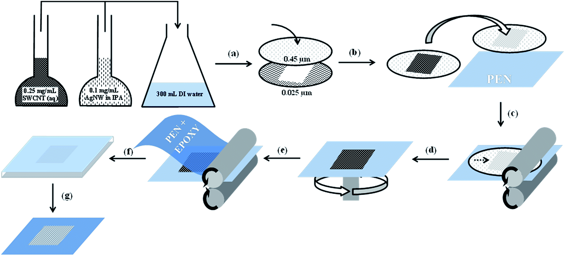 | ||
| Fig. 1 Schematic of laminator stamp and epoxy transfer method used to fabricate planar AgNW:SWCNT:PEDOT:PSS nanocomposite electrodes. (a) Filtering the AgNW and SWCNT solution; (b) transfer to PEN planar template; (c) stamp transfer through laminator; (d) peeling away the cellulose ester membrane; (e) coating with PEDOT:PSS and drying; (f) addition of an epoxy base layer and (g) peeling away the planar PEN template. | ||
Sheet resistance measurements were performed using the 4-point probe technique (KeithLink Technology Co., Ltd., New Taipei City, Taiwan). The values reported are an average of 10 measurements on two separate 64 mm2 samples. Flexibility testing was performed on a single planarized 25 mm2 electrode. 2-point probe measurements used during flexibility investigations were performed by placing two conducting epoxy pads on the electrode at a separation distance of 20 mm. Transmission and haze was measured on samples (25 mm2) using a Perkin-Elmer LAMBDA 950 UV/Vis/NIR Spectrophotometer with integrating sphere.
Scanning electron microscopy (SEM) images were acquired using a CamScan MX2500 (CamScan Optics, Cambridge, UK) working at an accelerating voltage of 10 kV and a working distance of 10 mm. The AgNW:SWCNT networks were stamp transferred onto a clean glass substrate and were imaged without a metal sputter coating to provide optimum contrast between the glass substrate, AgNWs and SWCNTs. Backscatter electron microscopy images were obtained at an accelerating voltage of 20 kV using an Inspect FEI F50 SEM with a field emission gun source and concentric backscatter detector.
Topographical atomic force microscope (AFM) measurements were acquired using a Bruker Multimode AFM with a Nanoscope V controller. NSC15 Mikromasch Silicon tapping mode probes with a nominal spring constant of 40 N m−1, resonant frequency of 325 kHz and tip radius equal to 10 nm were used. AFM images were acquired in tapping mode with all parameters including set-point, scan rate and feedback gains adjusted to optimize image quality and minimize imaging force. Roughness Rq values were obtained from 10 × 10 μm images after 3rd order plane fitting. Conductivity of the planar AgNW:SWCNT:PEDOT:PSS electrodes were mapped using peak force tunnelling AFM (PF-TUNA)31 on a Bruker Multimode AFM with a Nanoscope V controller. The software used to acquire all AFM data was version 8.15. The cantilevers used to obtain the PF-TUNA images were Bruker PF-TUNA conducting probes with a spring constant of 0.4 N m−1. The entire cantilever and tip is coated with 20 nm of each of platinum and iridium resulting in a total tip diameter of approximately 40 nm. PF-TUNA imaging parameters including set-point, scan rate, feedback gains, current sensitivity and applied bias were adjusted to optimize height and current image quality. The scanner was calibrated in the x, y, and z directions using silicon calibration grids (Bruker model numbers PG: 1 μm pitch, 110 nm depth and VGRP: 10 μm pitch, 180 nm depth).
Raman spectra and images were collected with a WiTEC alpha300R Microscope in confocal imaging Raman mode using a 100 × (numerical aperture 0.9) objective with a 532 nm Nd-YAG green (E = 2.33 eV) laser operating at constant power for each experiment. Laser power was kept at less than 10 mW during all measurements. Spectral images were acquired using an integration time of 5 s per pixel with each image composed of 50 pixels × 50 pixels. Each pixel corresponds to a separate Raman spectrum, allowing thousands of spectra to be acquired during an image scan. Raman images were generated by selecting a region, in each spectra, in which a material specific peak is observed. The intensity of the selected region was plotted relative to the x, y position of the scanning laser. Single spectra were also acquired at points on the Raman images with typical integrations times between 30 s to 60 s and 2 to 3 accumulations per spectra. The spectral resolution is approximately 3 cm−1. Raman data was collected by the WiTEC Control software and analyzed using the WiTEC Project software.
Device fabrication and testing
Organic solar cells with a structure of electrode/MoOx/poly(3-n-hexylthiophene-2,5-diyl) (P3HT):phenyl-C61-butyric acid methyl ester (PCBM)/Al were fabricated with ITO or planar AgNW:SWCNT:PEDOT:PSS as the transparent electrode. Pre-patterned ITO substrates (Xinyan Technology Ltd.) were cleaned using Alconox (Alconox) in de-ionized water. The ITO substrates were rinsed several times with de-ionized water and ultra-sonicated in de-ionized water for 5 min. The ITO substrates were then ultra-sonicated in acetone (HPLC grade) and IPA (HPLC grade) for 10 min each, followed by drying under a flow of nitrogen. MoOx (Sigma Aldrich, Australia) (20 nm) was deposited using a vacuum thermal evaporator at a pressure ∼10−6 mbar onto ITO and the planar AgNW:SWCNT:PEDOT:PSS electrodes during the same evaporation.A blend of P3HT:PCBM (1:1 w/w) was prepared by mixing equal amounts of individual solutions of P3HT (Mw = 94 kDa, PDI = 1.9) (Merck, USA) and PCBM (American Dye Source, USA) in anhydrous dichlorobenzene (DCB), with each solution having a concentration of 30 mg mL−1. The P3HT:PCBM solution was then filtered (0.22 μm PTFE filter, Membrane Solutions) and spin coated (500 rpm for 3 s, then 1400 rpm for 17 s) on top of the AgNW:SWCNT:PEDOT:PSS/MoOx or ITO/MoOx electrodes to get a thickness of ∼100 nm. The P3HT:PCBM film was then annealed on a hot plate. To investigate annealing conditions on device performance four different annealing conditions were used ((1) 60 °C, 20 min, (2) 120 °C, 10 min, (3) 150 °C, 5 min and (4) 180 °C, 2 min). Finally, a 100 nm layer of Al was deposited using a thermal evaporator at a pressure of ∼10−6 mbar to complete the device structure. The devices fabricated had an active area of 0.2 cm2, which was defined using a shadow mask during cathode evaporation. Post fabrication, the devices were annealed on a hot plate at 180 °C for 2 minutes.
Device characterization was performed using an Abet Triple-A (Abet Technologies) solar simulator. The solar mismatch of the xenon lamp (550 W Oriel) spectrum was minimized using an AM1.5G filter. Light intensity at ∼100 mW cm−2 AM1.5G was calibrated by using a National Renewable Energy Laboratory (NREL) certified standard silicon photodiode (2 cm2), with a KG5 filter. A Keithley® 2400 source measurement unit in a two wire configuration set-up was used for current density–voltage (J–V) measurements. At least five devices were characterized for each type of anode and for each fabrication condition. The short circuit current densities from J–V measurements of best devices were crossed checked with integrated current density from incident photon conversion efficiency (IPCE) measurements and they were within a difference of 10%. IPCE spectra were taken using a PV Measurement QEX7 setup, which was calibrated with an NREL certified photodiode and operated without white light bias and chopped and locked in the small perturbation limit.
All fabrication steps and testing of devices were done in a class 1000 cleanroom. Except for cleaning of the ITO substrates, all other steps for device fabrication and testing were done in an inert environment (MBraun glove box, O2 < 0.1 ppm; H2O < 0.1 ppm). The evaporations were carried out using a thermal evaporator connected to a glove box.
Results and discussion
Planar electrode fabrication process
Planar AgNW:SWCNT:PEDOT:PSS electrodes were fabricated via a scalable, R2R compatible, solution process using a lift off technique from a flexible substrate. Processes reported previously have relied upon the dissolution of a mixed cellulose ester membrane to transfer the AgNW:SWCNT network to a rigid substrate.29 In the process presented in Fig. 1, the relative adhesion of the AgNW:SWCNT network to various substrates was investigated and it was found that the interwoven network could be efficiently stamp transferred to rigid or flexible substrates when SWCNTs were co-deposited with AgNWs (Fig. 1(d)). After preparing a mixed dispersion of AgNWs and SWCNTs in de-ionized water, the process consisted of the following basic steps: (a) filtration through a masked cellulose ester membrane to create the desired interwoven pattern; (b) placing the cellulose ester filter on top of the planar PEN template; (c) passing the cellulose ester membrane/AgNW:SWCNT/PEN stack through heated rollers; (d) peeling away the cellulose ester membrane; (e) coating the PEN substrate and the interwoven electrode with PEDOT:PSS and drying; (f) addition of an epoxy base layer to adhere and transfer to another glass/plastic substrate and (g) peeling away the planar PEN template to reveal the electrode active surface. For a more detailed description of please see methods section.SWCNTs have previously been shown to wrap around the AgNWs during solution phase processing to create an interwoven self-supporting network.26 It is the strength of the interaction between AgNWs and SWCNTs that enables AgNW stamp transfer (Fig. 1(c)) to a substrate to occur, and which give its important properties. Fig. 2 shows a comparison of the sheet resistance of an electrode formed by the AgNW stamp transfer method with and without SWCNTs on glass. Measurements were taken after removal of the cellulose ester membrane (step (d), Fig. 1).
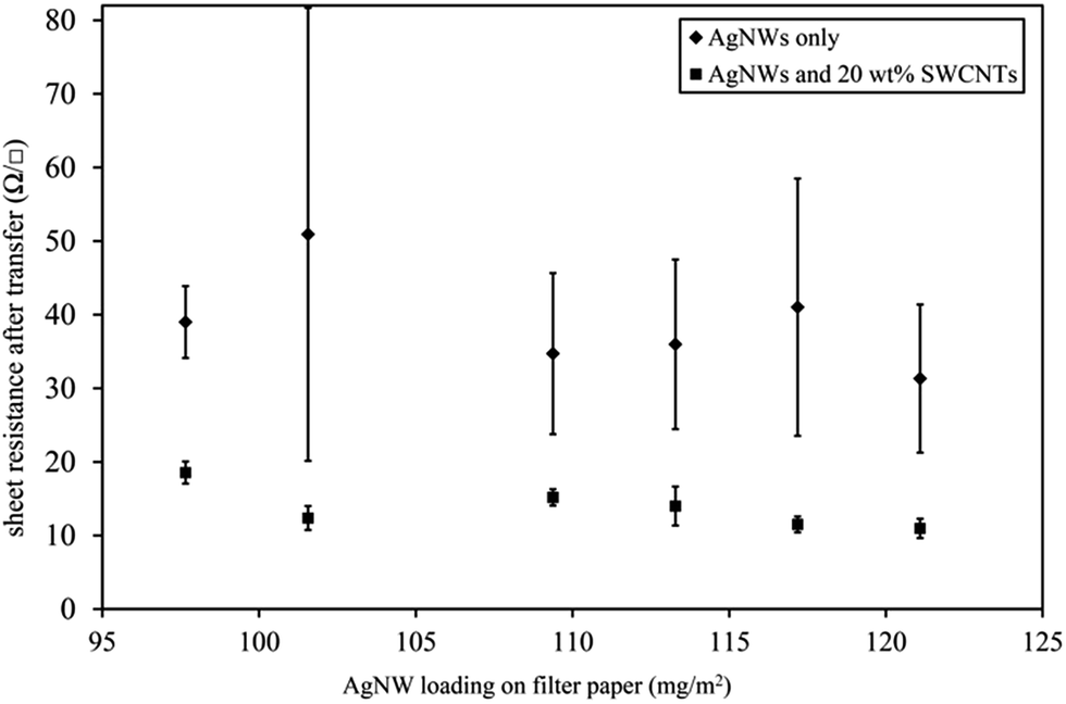 | ||
| Fig. 2 Sheet resistance of AgNW networks transferred from cellulose ester filter paper to PEN (Fig. 1, step (d)) without SWCNTs (diamonds) and with 20 wt% SWCNTs (squares). Values are an average of 20 measurements on 3 separate 8 × 8 mm electrodes. Error bars represent 1 standard deviation. | ||
The AgNW only film (Fig. 2, diamonds) produced a conducting network with a sheet resistance of approximately 30–50 Ω □−1 with a standard deviation of up to 30.8 Ω □−1. This is significantly poorer than the sheet resistance of commercial ITO on glass (10–15 Ω □−1) although it is similar to ITO on flexible substrates.32 Nevertheless, the sheet resistance is too high for large area devices. The error associated with each sample is large and reflects the poor reproducibility of the technique for AgNW only electrodes. The poor transfer is presumably due to weak attractive forces between the AgNW network and the glass substrate during lamination.
By co-depositing AgNWs with 20 wt% SWCNTs (Fig. 2, squares), significantly lower sheet resistivities are achievable (11–18 Ω □−1). The standard deviation of the SWCNTs assisted AgNW stamp transfer is much smaller (1.1–2.6 Ω □−1) reflecting the better reproducibility of the process.
SEM was conducted on the stamp transferred AgNW:SWCNT networks from mixed cellulose ester filter papers (0.4 μm) containing 109 mg m−2 loading with and without SWCNTs, shown in Fig. 3(a) and (b), respectively. In Fig. 3(a) it can be seen that without the presence of SWCNTs the AgNW forms a dense network after stamp transfer from the cellulose ester membrane. However, the sheet resistance (34.7 ± 10 Ω □−1) suggests that the network is not well interconnected after stamp transfer (Fig. 1, step (d)).
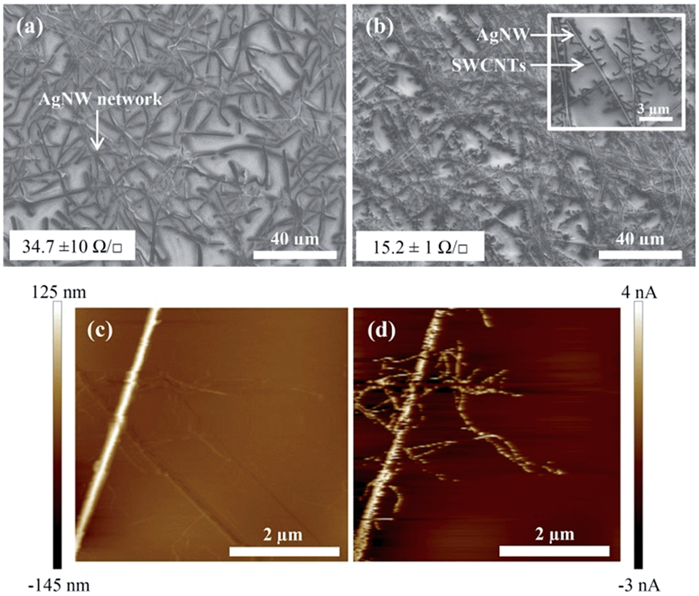 | ||
| Fig. 3 SEM images of stamp transferred AgNW networks before planarization on glass (a) without SWCNTs and (b) with SWCNT co-deposition. Inset in (b) is a higher resolution image showing contrast between AgNWs and SWCNTs on the glass substrate surface, (c) and (d) are the height and current channels from PF-TUNA, respectively. | ||
Fig. 3(b) shows a very high density of co-deposited AgNWs and SWCNTs on a the glass surface. The high resolution inset in Fig. 3(b) shows that every SWCNT is closely associated with the AgNW network leading to a sheet resistance significantly lower than that of the AgNW only network at 15.2 ± 1 Ω □−1. Fig. 3(c) and (d) are high magnification PF-TUNA images showing the height (Fig. 3(c)) and conductivity (Fig. 3(d)) of the AgNW:SWCNT electrode. Importantly, we can see from Fig. 3(d) that the SWCNTs and the AgNWs are electrically connected, which is beneficial for charge collection at the active surface of the electrode upon planarization.
Planar electrode properties
Upon completion of the planarization process (Fig. 1, step (g)) the active surface of the electrode had a sheet resistance of 4–7 Ω □−1 and an average transmission of >86% over wavelength range of 800–400 nm and a haze value of 11.6% over the same wavelength range (Fig. 4(c)). Importantly, the figure of merit is the same for electrodes produced on glass substrates as well as plastic film using the process outlined in Fig. 1 with values between approximately 344–400 Ω−1 which compares with between 48 and 208 Ω−1 for AgNW composites reported in the literature. The improvement over previous work (Table 1) is due to the reduction of fabrication steps by stamp processing the AgNW:SWCNT network and the ability to process on a PEN planar template instead of silicon.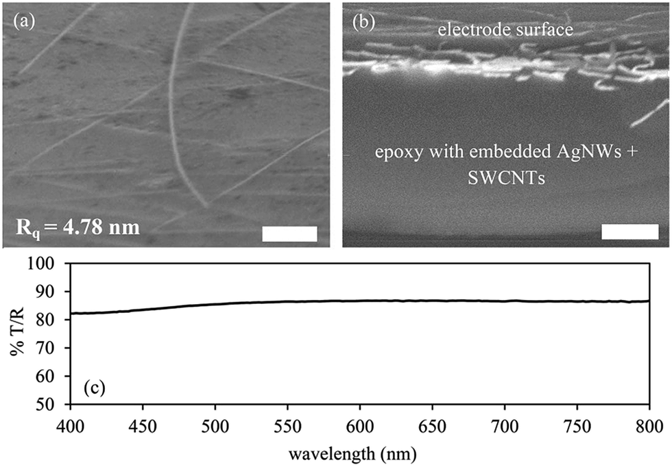 | ||
| Fig. 4 SEM micrographs of the AgNW:SWCNT:PEDOT:PSS (a) active surface at 70 degree tilt angle and Rq roughness as measures by AFM, (b) cross-section of electrode on a PEN flexible substrate. The scale bar is 2 μm for both images, (c) transmission spectra of planar electrode between 400 and 800 nm. | ||
| Composite material | Sheet resistance (Ω □−1) | Transmission at 550 nm (%) | Figure of merit | Reference |
|---|---|---|---|---|
| Poly(acrylate) | 7.5 | 79.6 | 208 | 33 |
| PEDOT:PSS | 10.8 | 84.3 | 187 | 34 |
| Healable polymer | 9.5 | 50.0 | 48 | 35 |
| Heat resistance polymer | 25.0 | 86.4 | 99 | 36 |
| PEDOT:PSS | 10.0 | 82.5 | 187 | 37 |
| Polyimide | 20.0 | 83.0 | 97 | 38 |
| PEDOT:PSS/SWCNTs | 6.6 | 86.0 | 367 | 29 [previous work] |
| PEDOT:PSS/SWCNTs | 4–7 | 80.0–86.0 | 344–400 | [This work] |
Evidence for the AgNW:SWCNT:PEDOT:PSS structure being present at the active surface of the electrode is shown in Fig. 4(a) and a cross-section of the electrode structure is shown in Fig. 4(b). The roughness of the electrode is 4.78 nm over a 10 × 10 μm plane fitted image. The cross-section image (Fig. 4(b)) shows that the overall thickness of the epoxy layer is approximately 5 μm.
Importantly, Fig. 4(b) shows that the AgNWs are present at the active layer and not found distributed throughout the epoxy.
Raman microscopy of the electrode surface revealed the position of PEDOT:PSS and SWCNTs relative to the AgNWs present at the surface of the electrode. An example Raman spectrum is shown in Fig. 5(d) and other spectra are included in the ESI.† In the optical image of Fig. 5(a) the silver nanowires are easily identified. However, the other components of the electrode namely, PEDOT:PSS and SWCNTs are not visible optically. By plotting the intensity of the Raman signal at 440 cm−1, which corresponds to the sulphonate bending from PSS,39 and 1597 cm−1, corresponding to the G band for SWCNTs,40 the regions on the electrode surface that contained PEDOT:PSS and SWCNTs, respectively can be identified. Fig. 5(b) shows the regions of PEDOT:PSS on the active surface of the electrode and indicates that PEDOT:PSS is present over the entire surface. Fig. 5(b) shows that the PEDOT:PSS signal is enhanced when in close association with AgNWs. This observation has two possible explanations. Firstly, since the PEDOT:PSS is spin-cast onto the AgNW network it may become trapped at the apex of adjoining nanowires and the planar PEN template resulting in a high concentration of PEDOT:PSS relative to the areas between the wires. Alternatively, it may be due to enhancement of the Raman signal at the surface of AgNWs.41,42 It is apparent that the SWCNTs on the surface of the electrode are present on the AgNWs as well as in between the nanowire network. It is unsurprising that there are significant quantities of SWCNTs in close association with the AgNWs since the solution phase deposition has been seen to encourage this interaction.26 The SWCNTs, which are spread out between the AgNW network are expected to increase the charge collecting capability of the electrode and also serve to connect and AgNW that are separate from the primary conducting network. Fig. 5(d) is single point Raman spectra collected at positions 1 and 2 as indicated on the optical image Fig. 5(a). The Raman spectra at position 1 shows a strong Raman signal at 1597 cm−1, which is assigned to the G-band typical for SWCNTs. A peak at 2680 cm−1 can also be observed which is characteristic of the 2D region for SWCNTs.40 The Raman spectra at position 2 does not show any of the characteristic Raman peaks for SWCNTs but instead shows Raman peaks typical for PEDOT:PSS.39,43,44
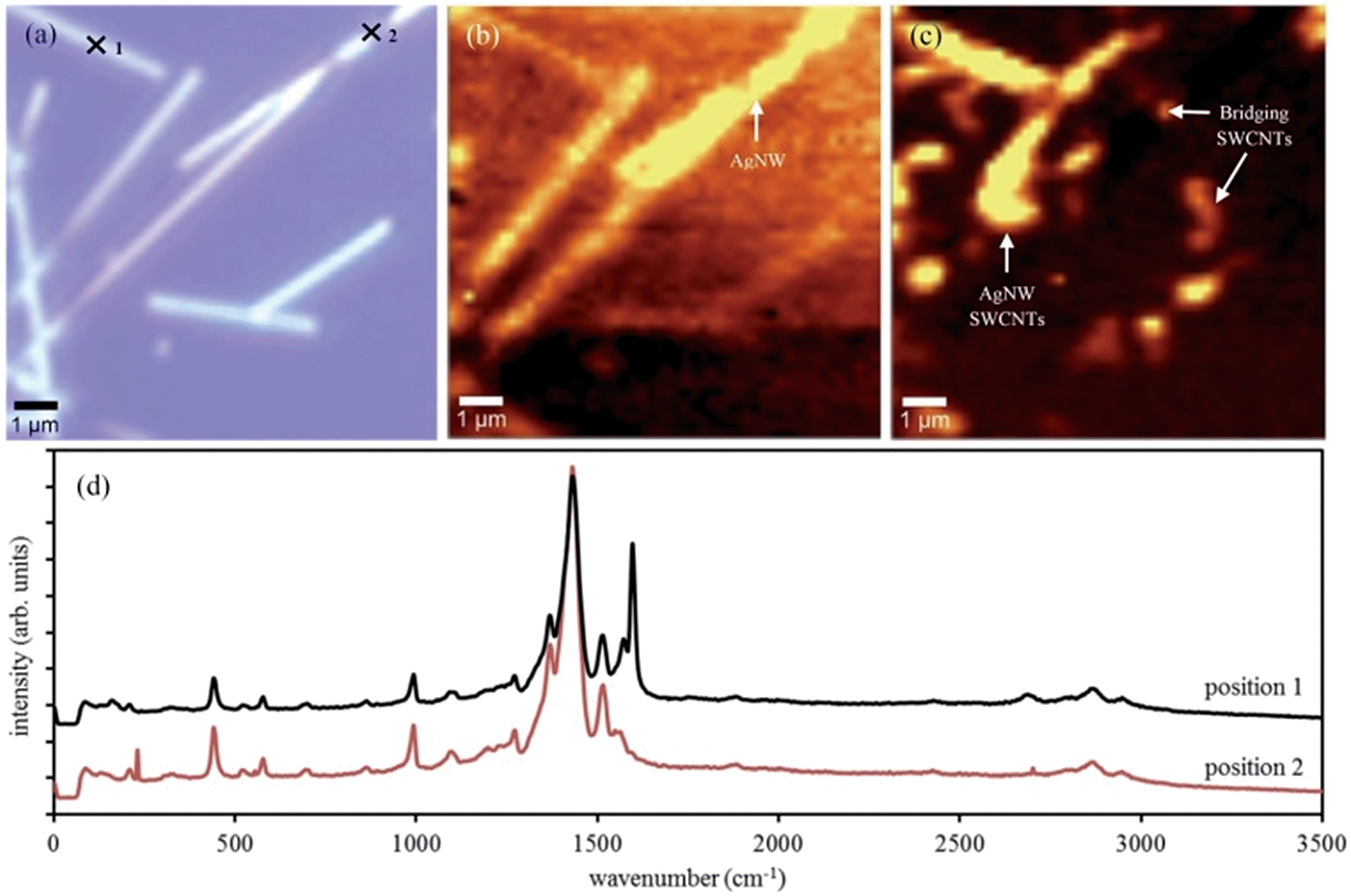 | ||
| Fig. 5 (a) Optical micrograph of a planar AgNW:SWCNT:PEDOT:PSS/PEN electrode surface (b) Raman image of PEDOT:PSS by plotting the intensity of the signal at 440 cm−1, (c) Raman image of SWCNTs by plotting the intensity of the signal at 1597 cm−1 as a function of the surface position, brighter regions correspond to higher signal intensity and (d) single point Raman spectra from positions 1 and 2 indicated on optical image (a). | ||
The planar AgNW:SWCNT:PEDOT:PSS electrodes on PEN were found to retain a low sheet resistance after bending at a radius of 5 mm up to 500 times (Fig. 6). After each bend cycle the sheet resistance of the electrode was measured using a four-point probe and from two conductive epoxy pads on the electrode at a separation distance of 20 mm. The open circles in Fig. 6 shows that the four-point probe measurement increases slightly over the 500 bend cycles, however, small indentations were left in the soft polymer electrode film after each measurement and are believed to contribute to this rise. To overcome this problem two conductive epoxy pads were placed on the electrode and used as stable contact points for resistance measurements using a multimeter (Fig. 6, open squares). The measurement shows that over the 500 bend cycles at a 5 mm bend radius there is no significant change in the resistivity of the electrode. The high flexibility of the planar AgNW:SWCNT:PEDOT:PSS/PEN electrode makes is suitable for R2R manufacturing processes and a range of organic optoelectronic applications.
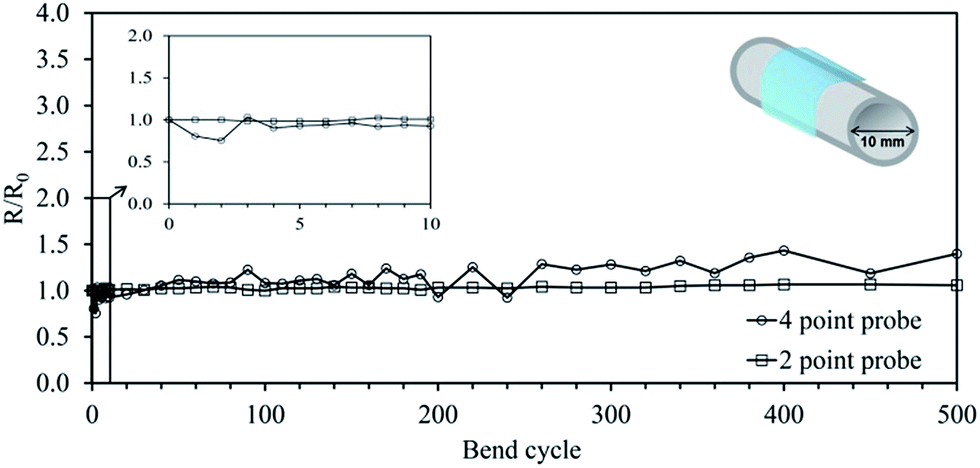 | ||
| Fig. 6 Change of sheet resistance of a AgNW:SWCNT:PEDOT:PSS/PEN planar electrode measured with four- and two-point probes. The samples were bent at a 5 mm radius 500 times. Expanded view shown of bend cycle 0–10 and inset a schematic of the bend radius used. | ||
OPV devices
The current density (J) and voltage (V) characteristics of the best devices fabricated on AgNW:SWCNT:PEDOT:PSS/glass and comparative ITO electrodes are shown in Fig. 7(a) and (b), respectively with the device statistics for each structure and annealing conditions given in Table 2. For the AgNW:SWCNT:PEDOT:PSS on glass electrodes, annealing for 10 min at 120 °C resulted in the best device performance, with a PCE of 1.85 ± 0.18%. For the same annealing condition the average ITO device efficiency was 2.2 ± 0.1%. On average, the devices fabricated with AgNW:SWCNT:PEDOT:PSS electrodes achieved ∼86% of the efficiency of comparable OPV devices fabricated with an ITO transparent electrode. Further improvements are expected once device fabrication parameters are fully explored.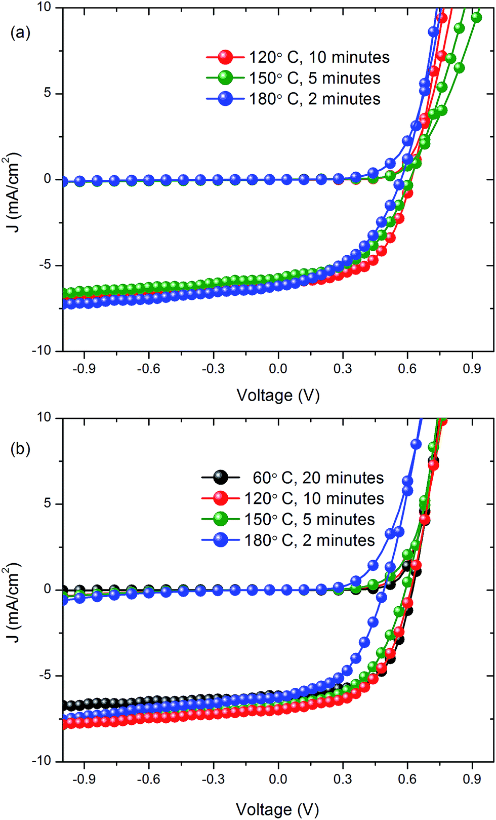 | ||
| Fig. 7 Current density versus voltage characteristics of devices with (a) AgNW:SWCNT:PEDOT:PSS/glass electrodes and (b) ITO/glass electrodes, respectively. | ||
| Annealing conditions | J sc (mA cm−2) | V oc (V) | FF | Eff. (%) | |
|---|---|---|---|---|---|
| AgNW:SWCNT:PEDOT:PSS | |||||
| 60 °C, 20 min | Average | — | — | — | — |
| Highest | |||||
| 120 °C, 10 min | Average | 5.7 ± 0.3 | 0.60 ± 0.00 | 0.54 ± 0.03 | 1.9 ± 0.2 |
| Highest | 6.1 | 0.60 | 0.58 | 2.1 | |
| 150 °C, 50 min | Average | 5.2 ± 0.4 | 0.60 ± 0.01 | 0.48 ± 0.02 | 1.5 ± 0.2 |
| Highest | 5.8 | 0.62 | 0.50 | 1.7 | |
| 180 °C, 2 min | Average | 5.6 ± 0.3 | 0.54 ± 0.01 | 0.48 ± 0.02 | 1.4 ± 0.1 |
| Highest | 6.2 | 0.56 | 0.50 | 1.6 | |
|
|||||
| ITO | |||||
| 60 °C, 20 min | Average | 6.2 ± 0.2 | 0.61 ± 0.01 | 0.59 ± 0.01 | 2.2 ± 0.10 |
| Highest | 6.3 | 0.6.2 | 0.60 | 2.3 | |
| 120 °C, 10 min | Average | 6.7 ± 0.4 | 0.60 ± 0.00 | 0.55 ± 0.02 | 2.2 ± 0.10 |
| Highest | 7.0 | 0.60 | 0.56 | 2.3 | |
| 150 °C, 50 min | Average | 6.7 ± 0.1 | 0.58 ± 0.01 | 0.51 ± 0.01 | 2.0 ± 0.1 |
| Highest | 6.8 | 0.58 | 0.52 | 2.0 | |
| 180 °C, 2 min | Average | 6.1 ± 0.2 | 0.47 ± 0.01 | 0.50 ± 0.01 | 1.4 ± 0.1 |
| Highest | 6.3 | 0.48 | 0.51 | 1.5 | |
An annealing temperature of 120 °C, which gave the best device performance on glass, is compatible with the use of flexible plastic substrates. A device fabricated on a flexible PEN substrate produced an efficiency of 1.2%, as shown in Fig. 8. This is the first time that a R2R compatible nanocomposite electrode has been used for fabrication of a flexible ITO device.
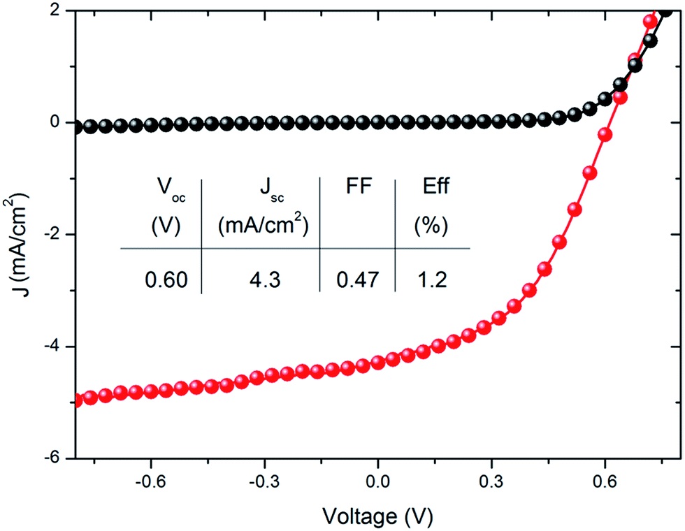 | ||
| Fig. 8 Current density versus voltage characteristics of device with AgNW:SWCNT:PEDOT:PSS electrode on flexible PEN along with the performance parameters. | ||
Conclusions
A roll to roll (R2R) compatible, solution process for the production of highly conductive, transparent and planar electrode based on silver nanowires (AgNW) and single walled carbon nanotubes (SWCNT) imbedded into PEDOT:PSS has been demonstrated, with a sheet resistance of 4–7 Ω □−1 and a transmission of >86% between 800 and 400 nm. The figure of merit of 344–400 Ω−1 is the highest published for AgNW composite electrodes.The low temperature, solution based process has been demonstrated to be able to produce electrodes with the same properties of both glass and flexible plastic (PEN) substrates with OPVs fabricated on the electrodes delivering ∼90% of the performance of equivalent ITO based devices on a glass substrate, this is without fabrication optimisation for the flexible electrode.
The process to fabricate the high figure of merit electrodes uses the entanglement of silver nanowires and single walled carbon nanotubes to provide sufficient mechanical stability to enable the transfer from a cellulose ester membrane.
The planar electrode surface structure exists as an interpenetrating network of AgNWs and SWCNTs imbedded in PEDOT:PSS with substantial concentrations of SWCNTs and PEDOT:PSS observed at the electrically active surface. In addition to active participation in charge collection and transport, the SWCNTs have also been demonstrated to facilitate the stamp transfer from a cellulose ester membrane to a receiving substrate by providing mechanical stability to the mesh with significantly improved consistency of transfer compared to a AgNW only mesh.
The planar AgNW:SWCNT:PEDOT:PSS electrode is highly flexible and resistance to fatigue with no degradation of the conductivity after bending at a radius of 5 mm up to 500 times opening the potential for use in novel applications and R2R fabrication of organic optoelectronic devices.
Acknowledgements
This work was supported by the CSIRO Future Manufacturing Flagship: Flexible Transparent Electrodes for Plastic Electronics Cluster which includes The University of Queensland, University of Technology, Sydney and Flinders University. The authors acknowledge the facilities, and the scientific and technical assistance, of the Australian Microscopy & Microanalysis Research Facility at Flinders University. PM is an Australian Research Council Discovery Outstanding Research Awardee, PLB is a University of Queensland Vice Chancellor's Research Fellow and AVE is a Flinders University Australian Research Council Future Fellow.Notes and references
- D. M. Tanenbaum, H. F. Dam, R. Rösch, M. Jørgensen, H. Hoppe and F. C. Krebs, Sol. Energy Mater. Sol. Cells, 2011, 97, 157–163 CrossRef PubMed.
- T. T. Larsen-Olsen, B. Andreasen, T. R. Andersen, A. P. L. Böttiger, E. Bundgaard, K. Norrman, J. W. Andreasen, M. Jørgensen and F. C. Krebs, Sol. Energy Mater. Sol. Cells, 2011, 97, 22–27 CrossRef PubMed.
- M. Manceau, D. Angmo, M. Jørgensen and F. C. Krebs, Org. Electron., 2011, 12, 566–574 CrossRef CAS PubMed.
- F. C. Krebs, Org. Electron., 2009, 10, 761–768 CrossRef CAS PubMed.
- S. Bae, H. Kim, Y. Lee, X. Xu, J.-S. Park, Y. Zheng, J. Balakrishnan, T. Lei, H. R. Kim, Y. Il Song, Y.-J. Kim, K. S. Kim, B. Ozyilmaz, J.-H. Ahn, B. H. Hong and S. Iijima, Nat. Nanotechnol., 2010, 5, 574–578 CrossRef CAS PubMed.
- W. Gaynor, J.-Y. Lee and P. Peumans, ACS Nano, 2010, 4, 30–34 CrossRef CAS PubMed.
- C. Guillén and J. Herrero, Thin Solid Films, 2011, 520, 1–17 CrossRef PubMed.
- S. Logothetidis, Mater. Sci. Eng., B, 2008, 152, 96–104 CrossRef CAS PubMed.
- C. Viespe, I. Nicolae, C. Sima, C. Grigoriu and R. Medianu, Thin Solid Films, 2007, 515, 8771–8775 CrossRef CAS PubMed.
- K. A. Sierros, N. J. Morris, K. Ramji and D. R. Cairns, Thin Solid Films, 2009, 517, 2590–2595 CrossRef CAS PubMed.
- E. J. Spadafora, K. Saint-Aubin, C. Celle, R. Demadrille, B. Grévin and J.-P. Simonato, Carbon, 2012, 50, 3459–3464 CrossRef CAS PubMed.
- J. L. Blackburn, T. M. Barnes, M. C. Beard, Y. Kim, R. C. Tenent, T. J. Mcdonald, B. To, T. J. Coutts and M. J. Heben, ACS Nano, 2008, 2, 1266–1274 CrossRef CAS PubMed.
- J. Garoz-Ruiz, S. Palmero, D. Ibañez, A. Heras and A. Colina, Electrochem. Commun., 2012, 25, 1–4 CrossRef CAS PubMed.
- S. Giurgola, P. Vergani, F. Lucchi and V. Pruneri, in Lasers and Electro-Optics, 2007 and the International Quantum Electronics Conference. CLEOE-IQEC 2007. European Conference on, 2007 DOI:10.1109/CLEOE-IQEC.2007.4386181.
- A. Kamyshny, J. Steinke and S. Magdassi, Open Appl. Phys. J., 2011, 4, 19–36 CrossRef CAS.
- E. C. Garnett, W. Cai, J. J. Cha, F. Mahmood, S. T. Connor, M. Greyson Christoforo, Y. Cui, M. D. McGehee and M. L. Brongersma, Nat. Mater., 2012, 11, 241–249 CrossRef CAS PubMed.
- V. Scardaci, R. Coull, P. E. Lyons, D. Rickard and J. N. Coleman, Small, 2011, 7, 2621–2628 CrossRef CAS PubMed.
- T. M. Barnes, M. O. Reese, J. D. Bergeson, B. a. Larsen, J. L. Blackburn, M. C. Beard, J. Bult and J. van de Lagemaat, Adv. Energy Mater., 2012, 2, 353–360 CrossRef CAS PubMed.
- A. R. Madaria, A. Kumar and C. Zhou, Nanotechnology, 2011, 22, 245201 CrossRef PubMed.
- W. Hong, Y. Xu, G. Lu, C. Li and G. Shi, Electrochem. Commun., 2008, 10, 1555–1558 CrossRef CAS PubMed.
- Q. Xu, T. Song, W. Cui, Y. Liu, W. Xu, S.-T. Lee and B. Sun, ACS Appl. Mater. Interfaces, 2015, 7, 3272–3279 CAS.
- J.-H. Lee, N.-R. Kim, B.-J. Kim and Y.-C. Joo, Carbon, 2011, 50, 98–106 CrossRef PubMed.
- K.-H. Ok, J. Kim, S.-R. Park, Y. Kim, C.-J. Lee, S.-J. Hong, M.-G. Kwak, N. Kim, C. J. Han and J.-W. Kim, Sci. Rep., 2015, 5, 9464 CrossRef CAS PubMed.
- S. B. Sepulveda-Mora and S. G. Cloutier, J. Nanomater., 2012, 2012, 1–7 CrossRef.
- H. Kim, C. M. Gilmore, A. Piqué, J. S. Horwitz, H. Mattoussi, H. Murata, Z. H. Kafafi and D. B. Chrisey, J. Appl. Phys., 1999, 86, 6451 CrossRef CAS PubMed.
- A. J. Stapleton, R. A. Afre, A. V. Ellis, J. G. Shapter, G. G. Andersson, J. S. Quinton and D. A. Lewis, Sci. Technol. Adv. Mater., 2013, 14, 035004 CrossRef.
- N. Vogel, J. Zieleniecki and I. Köper, Nanoscale, 2012, 4, 3820–3832 RSC.
- C. Priest, K. Jacobs and J. Ralston, Langmuir, 2002, 2438–2440 CrossRef CAS.
- A. J. Stapleton, S. D. Yambem, A. H. Johns, R. A. Afre, A. V. Ellis, J. G. Shapter, G. G. Andersson, J. S. Quinton, P. L. Burn, P. Meredith and D. A. Lewis, Sci. Technol. Adv. Mater., 2015, 16, 025002 CrossRef.
- M. N. Tchoul, W. T. Ford, G. Lolli, D. E. Resasco and S. Arepalli, Chem. Mater., 2007, 19, 5765–5772 CrossRef CAS.
- Bruker, Application Note # 132 Simultaneous Electrical and Mechanical Property Mapping at the Nanoscale with PeakForce TUNA.
- K.-H. Choi, J.-A. Jeong, J.-W. Kang, D.-G. Kim, J. K. Kim, S.-I. Na, D.-Y. Kim, S.-S. Kim and H.-K. Kim, Sol. Energy Mater. Sol. Cells, 2009, 93, 1248–1255 CrossRef CAS PubMed.
- W. Hu, X. Niu, L. Li, S. Yun, Z. Yu and Q. Pei, Nanotechnology, 2012, 23, 344002 CrossRef PubMed.
- D. Y. Choi, H. W. Kang, H. J. Sung and S. S. Kim, Nanoscale, 2013, 5, 977–983 RSC.
- C. Gong, J. Liang, W. Hu, X. Niu, S. Ma, H. T. Hahn and Q. Pei, Adv. Mater., 2013, 25, 4186–4191 CrossRef CAS PubMed.
- J. Li, J. Liang, X. Jian, W. Hu, J. Li and Q. Pei, Macromol. Mater. Eng., 2014, 299, 1403–1409 CrossRef CAS PubMed.
- S. Chen, Q. Cui and X. Guo, IEEE Trans. Nanotechnol., 2014, 14, 36–41 CrossRef.
- X. Guo, X. Liu, J. Luo, Z. Gan, Z. Meng and N. Zhang, RSC Adv., 2015, 5, 24953–24959 RSC.
- A. a. Farah, S. a. Rutledge, A. Schaarschmidt, R. Lai, J. P. Freedman and A. S. Helmy, J. Appl. Phys., 2012, 112, 113709 CrossRef PubMed.
- M. S. Dresselhaus, G. Dresselhaus, R. Saito and A. Jorio, Phys. Rep., 2005, 409, 47–99 CrossRef PubMed.
- J. L. Abell, J. D. Driskell and Y. Zhao, Chem. Commun., 2014, 50, 106–108 RSC.
- C. J. Orendorff, L. Gearheart, N. R. Jana and C. J. Murphy, Phys. Chem. Chem. Phys., 2006, 8, 165–170 RSC.
- A. Schaarschmidt, A. A. Farah, A. Aby and A. S. Helmy, J. Phys. Chem. B, 2009, 113, 9352–9355 CrossRef CAS PubMed.
- D. Mehtani, N. Lee, R. D. Hartschuh, A. Kisliuk, M. D. Foster, A. P. Sokolov and J. F. Maguire, J. Raman Spectrosc., 2005, 36, 1068–1075 CrossRef CAS PubMed.
Footnote |
| † Electronic supplementary information (ESI) available. See DOI: 10.1039/c5ta03248b |
| This journal is © The Royal Society of Chemistry 2015 |