
 Open Access Article
 This Open Access Article is licensed under a Creative Commons Attribution-Non Commercial 3.0 Unported Licence
Layered ternary sulfide CuSbS2 nanoplates for flexible solid-state supercapacitors†
Karthik
Ramasamy
*a,
Ram K.
Gupta
b,
Hunter
Sims
c,
Soubantika
Palchoudhury
d,
Sergei
Ivanov
a and
Arunava
Gupta
*d
aCenter for Integrated Nanotechnologies, Los Alamos National Laboratory, Albuquerque, NM-871851, USA. E-mail: kramasamy@lanl.gov
bDepartment of Chemistry, Pittsburg State University, Pittsburg, KS-66762, USA
cGerman Research School for Simulation Sciences, Jülich, Germany-52425
dCenter for Materials for Information Technology, The University of Alabama, Tuscaloosa, AL-35487, USA. E-mail: agupta@mint.ua.edu
First published on 28th May 2015
Abstract
Layer-structured materials are advantageous for supercapacitor applications owing to their ability to host a variety of atoms or ions, large ionic conductivity and high surface area. In particular, ternary or higher-order layered materials provide a unique opportunity to develop stable supercapacitor devices with high specific capacitance values by offering additional redox sites combined with the flexibility of tuning the interlayer distance by substitution. CuSbS2 is a ternary layered sulfide material that is composed of sustainable and less-toxic elements. We report the results of a systematic study of CuSbS2 nanoplates of varying thickness (4.3 ± 1.4 to 105 ± 5.5 nm) for use as supercapacitors along with the effect of ionic size of electrolyte ions on the specific capacitance and long-term cycling performance behavior. We have obtained specific capacitance values as high as 120 F g−1 for nanoplates with thickness of 55 ± 6.5 nm using LiOH electrolyte. Electronic structure calculations based on density functional theory predict that with complete surface coverage by electrolyte ions a specific capacitance of over 1160 F g−1 is achievable using CuSbS2, making it a very attractive layer-structured material for supercapacitor applications. Additionally, the calculations indicate that lithium ions can be intercalated between the van der Waals layers without significantly distorting the CuSbS2 structure, thereby further enhancing the specific capacitance by 85 F g−1. Quasi-solid-state flexible supercapacitor devices fabricated using CuSbS2 nanoplates exhibit an aerial capacitance value of 40 mF cm−2 with excellent cyclic stability and no loss of specific capacitance at various bending angles. Moreover, the supercapacitors are operable over a wide temperature range. We have further compared the electrochemical behavior of CuSbS2 with other non-layered phases in the system, namely Cu3SbS3, Cu3SbS4 and Cu12Sb4S13 that clearly highlight the importance of the layered structure for enhancing charge storage.
1. Introduction
The novel properties of layer-structured materials at the nano-scale offer exciting opportunities for the development of energy-relevant technologies.1,2 In recent years there has been renewed interest in investigating a variety of layered materials triggered in large part by the huge success of graphene.3–5 With reduced dimensions these materials often exhibit exceptional transport characteristics, mechanical stability and large surface area, which are essential for nano-dimensional electronics, catalysis, sensing and energy storage applications.1,6–9 The list of layer-structured materials that have been investigated include oxides, chalcogenides, carbides, nitrides, hydrides, hydroxides, phosphates, and phosphonates.10–12 Among them, the metal chalcogenides have been the most extensively studied because of their thickness-dependent quantum confinement effects resulting in enhanced optical and electrical properties at reduced thicknesses.1,13–15 An area that has thus far not received much attention is the use of layer-structured nanomaterials for supercapacitor applications. The large surface area and van der Waals gap can be exploited for the efficient adsorption and transport of electrolytes, which are desirable for charge storage and discharge processes.16,17Supercapacitors store and release energy instantaneously, possess long-term stability and are much safer to handle as compared to batteries.18 These characteristics make them attractive for use in electrical vehicles, consumer electronics, memory back-up systems and other applications where a burst supply of energy is required.19,20 Traditional supercapacitors based on carbonaceous materials work through the electrical double-layer capacitance mechanism that limits their energy density.21 A significant improvement in energy density can be achieved by use of metal oxide pseudocapacitors.22,23 However, their long-term stability is limited due to the volume change that occurs during charging and discharging processes and also unexpected secondary reactions that lead to degradation of the electrode materials.24–26 In contrast, layered materials that are separated by weak van der Waals forces can withstand large volume changes and can also host a variety of foreign atoms or ions between layers.27 Moreover, the graphene-like architecture in these materials is well suited for investigating unique transport properties at reduced dimensions.17,28,29 In this regard, a few layer-structured materials have been investigated for supercapacitor applications, including Ti3C2, MoS2 and SnSe.17,27,30 However, the investigations have thus far primarily focused on binary layered materials. Ternary or higher-order layered materials are potentially advantageous for supercapacitor applications over the binary ones as they offer additional redox sites (i.e., pseudo-capacitance sites) and greater tunability of the inter-layer distance by suitable substitution.31 These exceptional characteristics of ternary and higher order layered materials provide a unique opportunity to develop stable supercapacitor devices with high specific capacitance values.
With the aim of developing high stability supercapacitor devices based on ternary or higher-order layered materials, we have investigated copper antimony sulfide (CuSbS2), which is composed of sustainable and less-toxic elements. CuSbS2 is a ternary layered sulfide that crystallizes in an orthorhombic crystal system with Pnma space group.32,33 The crystal structure comprises of SbS2 and CuS3 interconnected chains that layer perpendicular to the c-axis. In each sheet, cage-like arrangements are formed by the stacking of six member S–Cu–S–Sb–S–Cu rings in a chair conformation adding to the existing van der Waals intercalation gap for intercalating atoms or ions.32,33 Because of its direct band gap at solar wavelengths and high absorption coefficient (>104 cm−1), CuSbS2 has been studied for solar cell applications.34–37 However, its unique capacity for intercalation have not been investigated for energy storage applications except in our recent preliminary study on mesocrystals of CuSbSexS1−x.38 Herein, we report results of a systematic study of CuSbS2 nanoplates with varied thicknesses for use in supercapacitors. In addition, we have investigated the effect of ionic size of electrolyte cations on the specific capacitance of CuSbS2 and its long-term cycling performance behavior. Our results indicate that significant enhancement in the supercapacitance values can be achieved using different thickness nanoplates as compared to previously reported mesocrystals of CuSbS2. For better understanding of the electrochemical properties we have determined the open-circuit voltage and specific capacity of CuSbS2 monolayers using first-principle calculations for different electrolyte cations. Based on the findings we fabricated quasi-solid-state flexible supercapacitor devices using CuSbS2 nanoplates that exhibit an aerial capacitance value of ∼40 mF cm−2 with excellent cyclic stability and no loss of specific capacitance at various bending angles. Moreover, we have investigated the temperature-dependent electrochemical behavior and charge–discharge characteristics of the CuSbS2 supercapacitor devices to evaluate their applicability over a wide temperature range. Finally, we have compared the electrochemical behavior of CuSbS2 nanoplates with nanocrystals of other phases in the Cu–Sb–S system, namely Cu3SbS3, Cu3SbS4 and Cu12Sb4S13 that clearly highlight the importance of the layered structure for enhancing charge storage. The applicability of CuSbS2 nanoplates both for solar energy conversion and energy storage applications bring them a step closer towards the fabrication of Single Component Solar Cell-SuperCapacitor (SC)3 devices.
2. Experimental section
2.1. Chemicals
All chemicals were used as received. Antimony chloride (SbCl3·6H2O, 99.5%) was received from Alfa Aesar; copper acetylacetonate (Cu(acac)2, ≥99.0%), and 1-oleylamine (OLA, ≥80–90.0%) were obtained from Acros Organics and Pfaltz and Bauer, respectively. Analytical grade hexane and ethanol were obtained from Aldrich Chemical Co.2.2. Synthesis of CuSbS2 nanoplates
For the synthesis of CuSbS2 nanoplates, Cu(acac)2 (0.5 mmol), SbCl3·6H2O (0.5 mmol) and oleylamine (OLA, 10 mL) were degassed and then backfilled with nitrogen. The reaction mixture was heated to targeted reaction temperature. In another vessel, sulfur (1.3 mmol) was dispersed in 1 mL of oleylamine. The sulfur solution was quickly introduced into the metal source mixture held at the synthesis temperature for 10–30 min. The product was isolated by addition of hexane (15 mL) and ethanol (15 mL) followed by centrifugation (4000 rpm/5 min). We also synthesized other Cu–Sb–S phases (Cu3SbS3, Cu3SbS4 and Cu12Sb4S13) in the form of nanocrystals for capacitance studies following procedures reported previously.362.3. Measurements
Transmission electron microscopy (TEM) analysis was performed using a FEI-Tecnai, 200 kV transmission electron microscope. Powder XRD patterns were recorded on a Bruker D8 instrument equipped with Cu Kα radiation source operated as a rotating anode at 40 kV and 20 mA. Scanning electron microscope (SEM) analysis was carried out using a JEOL 7000 FE SEM equipped with energy dispersive X-ray spectroscopy (EDX). The X-ray photoelectron spectroscopy (XPS) spectra were recorded using a Kratos Axis Ultra spectrometer employing a monochromated Al Kα X-ray source with analyzer pass energy of 80 eV for survey scans and 20 eV for elemental scans. Spectra were analysed by first subtracting a Shirley background and then obtaining accurate peak positions by fitting peaks using a mixed Gaussian/Lorentzian line shape. All photoelectron binding energies (BE) are referenced to C 1s adventitious peak set at 285 eV BE. The analyser was calibrated using elemental references; Au 4f7/2 (83.98 eV BE), Ag 3d5/2 (368.26 eV BE) and Cu 2p3/2 (932.67 eV BE).2.4. Methods (theory)
Calculations were performed using the Vienna ab initio Simulation Package (VASP)39–41 within the generalized gradient approximation of Perdew, Burke, and Ernzerhof (PBE) to density functional theory.42,43 We used the projected augmented-wave (PAW) pseudopotentials of Kresse and Joubert.44,45 and a plane wave cut off energy of 550 eV. The surface calculations were converged with respect to vacuum width (about 10 Å) and k-points (a 12 × 12 × 1 Monkhorst–Pack grid for a single unit cell), and all forces were minimized to within 0.05 eV Å−1. Positions of adatoms were optimized with the rest of the CuSbS2 surface remaining fixed. The open-circuit voltage was calculated on a 3 × 3 × 1 supercell to reduce inter-adatom interaction and compute the energy of formation of the surface with adsorbate via | (1) |
2.5. Electrochemical measurements
Electrochemical measurements were carried out using platinum wire and saturated calomel electrode (SCE) as counter and reference electrodes, respectively. The working electrode was obtained by mixing of CuSbS2 nanoplates (80 wt%), acetylene black (10 wt%) and polyvinylidene difluoride (PVDF, 10 wt%) in N-methyl-2-pyrrolidinone (NMP) and pasting onto a nickel foam, followed by drying at 60 °C under vacuum. KOH, NaOH and LiOH (3 M) were used as electrolytes. The charge storage capacity of the materials was tested using cyclic voltammetry (CV) and galvanostatic charge–discharge methods.46 The specific capacitance (Csp) values from charge–discharge measurements were calculated using the following expression.47 | (2) |
3. Results and discussions
Nanoplates of CuSbS2 have been synthesized following our earlier reported procedure.31 In brief, 1 mL of sulfur in oleylamine was introduced into the reaction mixture of Cu(acac)2 and SbCl3 in oleylamine at 170 °C. The reaction produced nanoplates with thickness of 4.3 ± 1.4 nm and edge dimensions of about 450 nm for 10 min reaction time. Reactions at higher reaction temperatures and longer reaction times produce thicker plates, with the lateral dimensions being closely maintained. The CuSbS2 structure consists of quadruple layers bound together by van der Waals forces (Fig. 1(a)). The Sb in one layer and S in the adjacent layer of the structure are separated by a distance of ∼3.115 Å, which is larger than the interlayer gap distance (2.051 Å). An expanded portion of one of the layers is shown in Fig. 1(b). A cage-like arrangement formed by stacking of six member (S–Cu–S–Sb–S–Cu) rings in chair conformation is apparent from the structure. The distances between two atoms of the same type in the cages are between 5.3 Å and 6.19 Å.32 Powder X-ray diffraction (XRD) was used for the determination of phase purity. Diffraction peaks corresponding to the orthorhombic structure of CuSbS2 are observed, with no trace of the binary sulfides of copper or antimony. XRD patterns in Fig. 1(c) obtained from CuSbS2 nanoplates synthesized at different temperatures are in good agreement with orthorhombic CuSbS2 phase (ICDD: 044-1417). Furthermore, the FWHM value of each peak decreases with increasing growth temperature, indicating increase in the crystallite size. In order to characterize the chemical constituents on the surface, we have carried out X-ray photoelectron spectroscopy (XPS) measurements on the CuSbS2 nanoplates. The qualitative XPS survey spectrum for CuSbS2 nanoplates is provided in Fig. S1(a).† The surface survey spectrum exhibits peaks corresponding to Auger electron ejection for Cu, Sb and S, along with C and O. No peaks from any other impurities were observed. High resolution XPS spectra in Fig. S1(b)–(d)† of Cu 2p, Sb 2p, S 2p from CuSbS2 nanoplates confirm the expected oxidation state of each element. The binding energy peaks at 930.3 eV and 950.2 eV, with an energy difference of 19.9 eV, can be assigned to 2p3/2 and 2p1/2 of Cu(I). For Sb(II), the doublet peaks at 528.3 eV (3d5/2) and 537.4 eV (3d3/2) with an energy separation of 9.1 eV are observed. High resolution XPS peaks for sulfur as a sulfide appear at 161.4 eV (2p3/2) and 162.6 eV (2p1/2) with a small energy difference of 1.2 eV.48 We have additionally estimated the elemental composition of the nanoplates using scanning electron microscopy-energy dispersive X-ray spectroscopy (SEM-EDX). The analysis results provide a composition ratio of 1![[thin space (1/6-em)]](https://www.rsc.org/images/entities/char_2009.gif) :1:1.95 (Cu:Sb:S) for the nanoplates with a slight deficiency in sulfur content.
:1:1.95 (Cu:Sb:S) for the nanoplates with a slight deficiency in sulfur content.
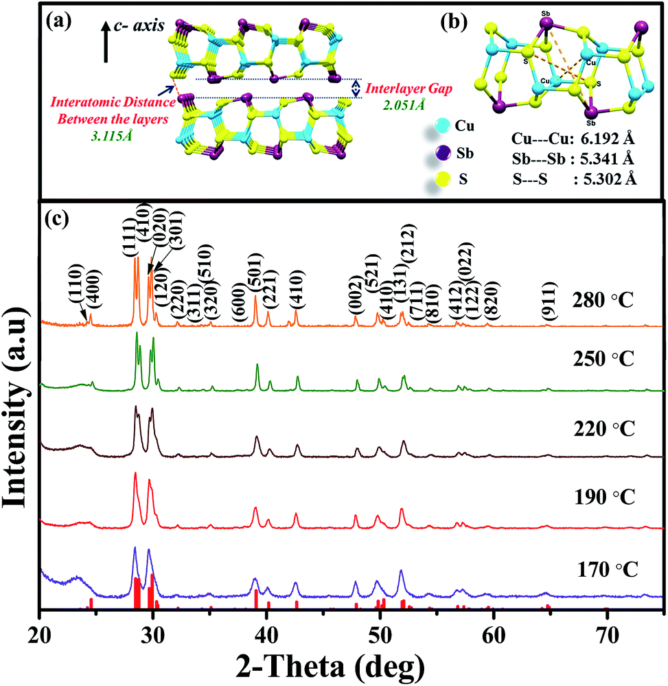 | ||
| Fig. 1 Crystal structures of CuSbS2 showing (a) the interlayer (van der Waals) gap and distance between two quadruple layers, and (b) cages within a single layer, (c) powder X-ray diffraction patterns of CuSbS2 nanoplates synthesized at different temperatures. The standard ICDD pattern (red lines; ICDD: 044-1417) of orthorhombic CuSbS2 is provided at the bottom. | ||
Transmission electron microscope (TEM) was used in the identification of nanocrystals morphology and size. Plate-like morphology was observed from TEM images in Fig. 2(a)–(d). The edge–edge length of the nanoplates varied from 400 ± 25 nm to 450 ± 20 nm for the growth time between 10 and 30 min at 170 °C with thickness from 4.3 ± 1.4 nm and 10.0 ± 0.7 nm (Fig. 2(e)–(l)). At higher temperatures (190–280 °C) the sizes were found to be between 300 ± 20 nm and 335 ± 25 nm and thickness of 19 ± 1 nm to 105 ± 5.5 nm. Average lattice distance (0.302 ± 0.003 nm) of the surface of nanoplates obtained from HRTEM image in Fig. S2(a)† are in very well agreement with the (200) planes of orthorhombic CuSbS2.
 | ||
| Fig. 2 (a)–(d) Top view and (e)–(h) side view TEM images. (i)–(l) Side view HRTEM images of different thickness CuSbS2 nanoplates. | ||
The electrochemical properties of nanoplates with different thickness were investigated by cyclic voltammetry and galvanostatic charge–discharge methods. Fig. 3(a) shows the cyclic voltammetry (CV) curves of different thickness CuSbS2 nanoplates at a scan rate of 50 mV s−1 using KOH as the electrolyte. A pair of reversible redox waves indicating the pseudocapacitance feature at essentially the same potential values is apparent from the CV curves of different thickness CuSbS2 nanoplates (Fig. 3(a)). With increasing scan rate, the CV curves maintain their shapes but exhibit increased peak currents (Fig. S3†). A concurrent increase in the ΔEwave (difference between Eap and Ecp) value is observed with a linear relationship for the wave current as a function of the square root of scan rate (Fig. S4†), indicating diffusion-controlled reaction kinetics during the redox process. From the CV curves in Fig. 3(a) a systematic increase in the current density can be noted with increasing nanoplate thickness followed by a decrease for the largest thickness, with the 55 ± 6.5 nm thick nanoplates displaying the highest current density. The thinner nanoplates are expected to exhibit higher current density due to the larger available surface area for redox reactions, but here we observe a reverse trend. From the analysis of the SEM and TEM images (Fig. S5† and 2, respectively) it appears that the thin plates readily aggregate, which leads to reduction of their surface area and, as such, to the reduction of the current density. As the thickness of plates increase, their agglomeration diminishes, leading to an increase in the surface area. However, further increase in nanoplate thickness again leads to decrease in the surface area and a consequent decrease in the current density. The current density trend with increasing thickness of the nanoplates trend is also reflected in the specific capacitance values deduced from CV curves at various scan rates.
 | ||
| Fig. 3 Cyclic voltammogram curves of (a) different thickness CuSbS2 nanoplates. (b) Galvanostatic charge–discharge characteristics of 55 ± 6.5 nm thick CuSbS2 nanoplates at different applied current. (c) Variation in specific capacitance of different thickness CuSbS2 nanoplates with applied current. (d) Ragone plot for different thickness nanoplates. (e) Cyclic voltammogram curves showing cyclic stability of 7.2 ± 1.4 nm CuSbS2 nanoplates. All the data were obtained with using KOH as electrolyte. | ||
We have additionally studied the charge storage capacity of CuSbS2 electrodes using galvanostatic charge–discharge measurements at various applied current. The representative discharge characteristics of CuSbS2 nanoplate (7.2 ± 1.4 nm) electrode is shown in Fig. 3(b) as a function of discharge current. As seen, the discharge time decreases with increasing discharge current. The variation of specific capacitance with discharge current for nanoplates of different thicknesses is shown in Fig. 3(c). The Csp values for 55 ± 6.5 nm thick nanoplates with KOH as electrolyte are determined to be 100, 96, 94, 92, 89, 92, 99 F g−1 at applied currents of 0.4, 06, 0.8, 1, 2, 3, 4 mA, respectively. The energy density and power density values (Ragone plot) calculated using the respective specific capacitance values is given in Fig. 3(d). These values are higher than those for CuSbE2 (E = S or Se) mesocrystals and comparable to the specific capacitance values reported for other chalcogenide nanocrystals (SnSe, CoS, CuS).30,38,49,50 The observed decrease in specific capacitance with increasing discharge current in some cases is likely due to higher potential drop and incomplete Faradic redox reaction of the active materials at higher discharge currents.
We investigated the long term cyclic stability of CuSbS2 nanoplate electrodes by carrying out CV measurements up to 1000 cycles. The representative CV curves of 7.2 ± 1.4 nm thick nanoplates are shown in Fig. 3(e). The wave profile and the area of the voltammograms appear to remain essentially unchanged, indicating the high cyclic voltammetric stability of the nanoplates without any significant volume change. Furthermore, the absence of additional redox waves in the CV curves confirms the absence of any new redox species in the process of CV cycling. However, a systematic increase in the reduction potential can be seen with increasing number of CV cycles suggesting increased intercalation of electrolyte ions between the layers.
Layer-structured materials are known to host atoms or ions that are smaller than the interlayer gap. CuSbS2 is a ternary layered sulfide material having an interlayer gap of 2.051 Å, sufficiently wide to host atoms or ions between the layers. Depending on the size of intercalates in the electrolytes, the specific capacitance of the material can be varied. With this perspective, we have carried out cyclic voltammetry measurements using LiOH, NaOH and KOH electrolytes. Fig. 4(a) shows CV measurements on CuSbS2 electrode using these three electrolytes. It can be noticed from the CV curves that the electrolyte with the smallest cationic radii (LiOH) has the highest reduction potential value. Indeed, the reduction potential exhibits an inverse relationship with the size of the electrolyte cation. Being the smallest ion, it is likely that Li+ most effectively intercalates between the layers and inside of the crown-like cages of CuSbS2. Because of the deeper intercalation, higher potential is required for Li+ reduction. The specific capacitance values determined from the charge–discharge characteristics of CuSbS2 nanoplates (55 ± 6.5 nm) at various applied currents using the three different electrolytes are provided in Fig. 4(b). The trend in specific capacitance values parallel the CV results, with LiOH showing the highest specific capacitance. We obtained specific capacitance values of 115–120 F g−1 at applied current values from 0.6–5 mA, with noticeably higher specific capacitance than those obtained for NaOH and KOH (Ragone plot of power density versus energy density is given in Fig. 4(c)). Furthermore, we have tested the cyclic stability of CuSbS2 nanoplates in these electrolytes using galvanostatic charge–discharge characteristics. Fig. 4(d) shows the cyclic stability of CuSbS2 electrode consisting of 55 ± 6.5 nm thick nanoplates using LiOH as electrolyte. A gradual increase in specific capacitance followed by the retention of essentially 100% of its value is observed even after 1000 cycles of charge–discharge measurements in LiOH. However, in the case of KOH an amplification of specific capacitance is recorded with increase of specific capacitance nearly by 47% on continuing the charge–discharge up to 5000 cycles (Fig. 4(e) and 5(a)). This is noteworthy since most other oxide and chalcogenide-containing supercapacitor materials severely lack long-term cyclic stability. The observed increase in specific capacitance using KOH electrolyte is likely caused by gradual intercalation of K+ ions between the layers or possible intercalation and exfoliation of the layers. This phenomenon relating to intercalation of electrolyte ion has been reported for the similar layered structure materials MoS2 supercapacitor using NaOH as electrolyte.17Fig. 5(b) shows the Ragone-plot of the specific capacitance with number of cycles. The plot shows an initial gradual increase in the energy density with power density up to about 1100 cycles followed by a sharp energy density increase from 2.6 W h kg−1 (1100th cycle) to 3.8 W h kg−1 (5000 cycles). The observed increase in energy density with increasing number of cycles further supports the proposed model of intercalation of electrolyte ions between the layers of CuSbS2. The inset to Fig. 4(d) shows the last few charge–discharge cycles for the CuSbS2 (55 ± 6.5 nm) nanoplates electrode.
 | ||
| Fig. 4 (a) Cyclic voltammogram curves of CuSbS2 nanoplates using different electrolytes. (b) Variation of specific capacitance of CuSbS2 nanoplates with applied current in different electrolytes. (c) Ragone plot for different thickness nanoplates. (d) Cycling performance of the CuSbS2 nanoplates at a constant current of 0.5 mA using LiOH electrolyte. The inset shows the first few cycles of the charge–discharge curves. (e) Cycling performance of 55 ± 6.5 nm CuSbS2 nanoplates at a constant current of 0.5 mA using different electrolytes. | ||
 | ||
| Fig. 5 (a) Cycling performance of the CuSbS2 nanoplates at a constant current of 0.5 mA using KOH electrolyte up to 5000 cycles. (b) Ragone plot showing variations of energy density and power density with respect to number of cycles. | ||
To better understand the interaction of different electrolyte ions with CuSbS2, we have determined the open-circuit voltage (OCV) and specific capacity of CuSbS2 monolayers within density functional theory framework. Optimization of the adatom positions (Li+, Na+ or K+) indicates the preferred location of the ions over the copper sites rather than the S or Sb sites. In Fig. 6(a), we have plotted the valence charge densities (relative to the unbonded densities) for all three 3 × 3 × 1 systems. All three indicate charge transfer from the adsorbed ion to the surface. The partial densities of states for the adatoms (Fig. 6(b)) lend support to the picture suggested by the charge densities: the valence s electron is almost completely transferred to the host system.
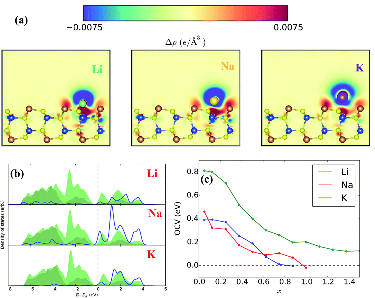 | ||
| Fig. 6 (a) Valence charge density for Li, Na, and K adsorbates with respect to the charge density of non-interacting species, nonbonded density, plotted in the plane of the adsorbed ion. Cu sites are blue, Sb are orange, and S are yellow, (b) partial density of states projected onto Li, Na, K (bottom) valence (n − 1)s orbitals (blue line), compared to the total (light green) and S-projected (dark green) DOS. The ionic ns orbital is nearly empty in all cases and shows some hybridization with the valence S 3p bands. (c) OCV vs. x for Li (blue), Na (red), and K (green) adsorption. x = 0.5 corresponds to complete monolayer coverage of the Cu sites. Higher x gives coverage of S (until x = 1.0) and Sb sites on a single side. | ||
We compute the OCV over a Cu site for Li, Na, and K ions adsorbed onto the CuSbS2 surface to be 0.390 eV, 0.461 eV, and 0.812 eV, respectively. These values follow the expected trend for adsorbed ions of increasing size but do not agree with Fig. 5(a). Instead, the measured behavior may indicate that intercalation rather than adsorption is dominant, as larger ions could be more difficult to accommodate between layers. This is evident in our relaxed intercalated structures: Na and K ions seem to displace the nearest Sb ion, driving it into the “bulk” of the layer (see ESI Fig. S6†). We find that Li, Na, and K have intercalation voltages (compared to the undisrupted host system) of 0.228 eV, 0.909 eV, and 0.581 eV. This non-monotonicity reflects the greater energy cost of distorting the CuSbS2 system to allow the intercalated K ions, but we still do not recover the observed behavior. It is possible that the fully relaxed intercalated structures cannot be achieved in the real many-layer nanoplates. Our calculations do show that the intercalation energies can scale inversely with ionic radius, and partial relaxation would enhance this trend.
The theoretical specific capacity can be estimated via51

With the aim of developing flexible, quasi-solid-state supercapacitors composed of cost effective and less-toxic materials, we have fabricated supercapacitor devices using LiOH/KOH electrolyte separating two CuSbS2 electrodes coated on Ni foam. A schematic representation of the device is shown in Fig. 7(a). The CV curves of the device at different scan rates are nearly symmetrical and rectangular without presence of any redox peaks (Fig. 7(b)). The CV curve characteristics are comparable to devices reported using other materials.16 The areal capacitance of the device deduced from CV curves at different scan rates is estimated to be 40 mF cm−2 at 25 mV s−1, which is significantly higher than that for supercapacitor devices fabricated using SnSe and SnSe2 nanoplates and comparable to MoS2-based device.17,30Fig. 7(c) shows cyclic voltammetry measurements of the quasi-solid-state device up to 4000 cycles at constant scan rate. The excellent electrochemical stability of the device is verified by the absence of redox waves and no visible changes in CV curve shapes and redox currents even after the 4000th cycle when compared with the initial curve. Further to this, galvanostatic charge–discharge measurements on the device have been carried out up to 2500 cycles at a constant current in order to investigate its cycling performance (Fig. 7(d)). The cyclic performance of a supercapacitor device can be described by two main processes, namely the activation and steady state. The activation period in our device lasts nearly up to 400 cycles with close to 50% increase in the specific capacitance value, as also observed for the CuSbS2 electrodes. In general, this activation period is significantly longer than, is commonly observed. The prolonged activation period further supports the notion of intercalation of electrolyte ions between the layers and within the cages of CuSbS2 electrodes. Interestingly, the specific capacitance value is unchanged even after 2500 cycles confirming the device's exceptional stability. In addition, the flexibility of the device has been investigated by measuring the CV curves at various bending angles. As shown in Fig. 7(e), the CV curves do not show any noticeable changes at bending angles of 15, 30 and 45° as compared with the CV curve without any bending. These results clearly demonstrate the potential applicability of CuSbS2 as a flexible, stable charge storage and delivery system (bending studies of electrode is given in Fig. S7†).
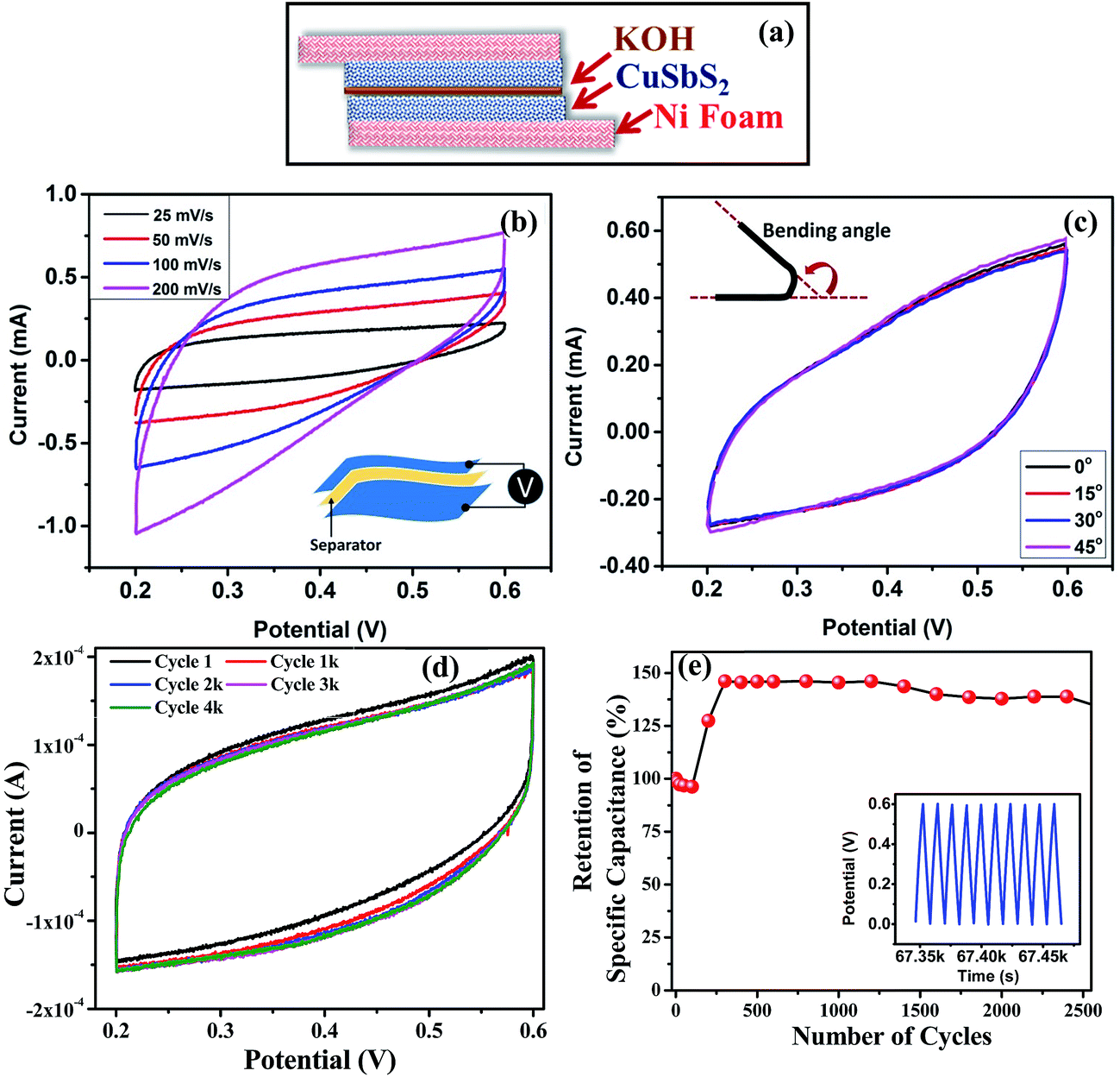 | ||
| Fig. 7 (a) Schematic of flexible quasi-solid-state supercapacitor device fabricated using 55 ± 6.5 nm CuSbS2 nanoplates. (b) Cyclic voltammogram curves of CuSbS2 nanoplates supercapacitor device at different scan rates using KOH. (c) Cyclic voltammogram curves of CuSbS2 nanoplate supercapacitor device at different bending angles. (d) Cyclic voltammogram curves showing cyclic stability of CuSbS2 nanoplates device. (e) Cycling performance of the CuSbS2 nanoplates supercapacitor device at a constant current of 1 mA. The inset shows the first few cycles of the charge–discharge curves. | ||
It is important to develop supercapacitors that can be used under a wide range of environmental conditions. Temperature is clearly one of the major factors that affect device performance. Considering this, we have investigated the electrochemical behavior of our supercapacitor devices at different temperatures. Fig. S8(a)† shows CV curves of a quasi-solid-state flexible device measured at different temperatures. A systematic increase in the redox current with increasing temperature is apparent from the CV curves, which is reflected in the areal specific capacitance values estimated from CV curves. The highest specific capacitance value is obtained at 55 °C, which is nearly 80% higher than the value at room temperature (Fig. S8(b)†). The specific capacitance obtained below room temperature (15 °C) is somewhat lower (by ∼8%) than that at ambient conditions. Despite temperature-dependent changes in specific capacitance values, the CV curves show nearly identical symmetrical shape without appearance of any redox waves at any temperature indicating thermal electrochemical stability of the device. Similar temperature-dependent changes in specific capacitance have also been observed in galvanostatic charge–discharge characteristics of the CuSbS2 supercapacitor device at different temperatures (Fig. S8(c) and (d)†).
Extending our investigations of Cu–Sb–S for supercapacitor applications, we have carried out cyclic voltammetry and galvanostatic charge–discharge measurements on nanocrystals of Cu3SbS3 (skinnerite), Cu3SbS4 (fematinite) and Cu12Sb4S13 (tetrahedrite) phases. These phases crystallize in non-layered structures: Cu3SbS3 in monoclinic, Cu3SbS4 in tetragonal and Cu12Sb4S13 in cubic form. Comparing the electrochemical behavior of these compounds with CuSbS2 nanoplates, it is possible to appreciate the importance of the layered structure for charge storage applications. We have recently reported the phase-pure synthesis of all four phases of Cu–Sb–S nanocrystals.36 Following these methods, we have synthesized spherical shape Cu3SbS3, oblate Cu3SbS4 and hollow structure Cu12Sb4S13 nanocrystals. Representative TEM images of these nanocrystals along with their crystal structures are given in Fig. 8(a)–(d). The specific capacitance values determined from charge–discharge characteristics (in KOH) using these nanocrystals as electrodes and corresponding Ragone plot are shown in the Fig. 8(e) and (f). From the figures it is apparent that all these nanocrystals exhibit low specific capacitance in comparison with CuSbS2 nanoplates, despite having similar compositions and sizes. This clearly illustrates that the layered structure is responsible for efficient insertion and extraction of electrolyte ions during the electrochemical process. Nevertheless, all the non-layered Cu–Sb–S compounds show very good cyclic stability (Fig. 9). We also studied the effect of electrolyte ions size on specific capacitance of Cu12Sb4S13 using KOH and LiOH electrolytes and did not observe any appreciable difference in their electrochemical behavior, supporting our conclusion of intercalation of electrolyte ions between the layers in the layer-structured CuSbS2 nanoplates.
 | ||
| Fig. 8 (a)–(d) Crystal structure and TEM images of different phases of Cu–Sb–S. (e) Variation of specific capacitance of different phases of Cu–Sb–S nanocrystals with applied current. (f) Ragone plot showing energy density vs. power density for the different Cu–Sb–S phases. | ||
 | ||
| Fig. 9 (a) Cycling performance of nanocrystals of CuSbS2, Cu12Sb4S13, Cu3SbS3 and Cu3SbS4 using KOH. | ||
4. Conclusion
We have systematically studied the effect of thickness on the electrochemical behavior and specific capacitance of CuSbS2 nanoplates. Electrochemical measurements reveal that nanoplates with thickness of 55 ± 6.5 nm are optimum for obtaining the highest specific capacitance. In addition, we have studied the specific capacitance of CuSbS2 nanoplates and their long-term cycling performance behavior using different electrolytes, namely LiOH, NaOH and KOH, and found that LiOH provides specific capacitance values as high as 120 F g−1. Further, to understand the interaction of different electrolytes with CuSbS2, we computed the electronic structure using density functional theory. Our calculations predict that the electrolyte cations prefer Cu-sites, and with only the Cu-sites occupation, theoretical specific capacitance of 387 F g−1 can be obtained with all three electrolytes. Interestingly, with complete coverage of CuSbS2 surface we obtain specific capacitance of 619, 697, and more than 1160 F g−1 for Li, Na and K respectively. These values are significantly higher than for any layer structured material investigated thus far. In addition, we have found that lithium ions can be intercalated between the van der Waals layers without distorting the CuSbS2 structure. With lithium ion intercalation, the specific capacitance can further be enhanced by 85 F g−1. These investigations strengthen our hypothesis that multiple site adsorption and intercalation can be collectively realized in the ternary layered materials. Our preliminary effort on fabricating quasi-solid-state flexible supercapacitor device using CuSbS2 nanoplates have provided an aerial capacitance value of 40 mF cm−2 with excellent cyclic stability and no loss of specific capacitance at various bending angles, with operability over a wide temperature range. Our comparative study of CuSbS2 nanoplates with non-layer structure phases in the Cu–Sb–S system Cu3SbS3, Cu3SbS4 and Cu12Sb4S13 clearly highlight the importance of the layered structure for enhancing charge storage. The remarkable theoretical capacitance with excellent cyclic stability in corrosive electrolytes and direct gap visible light absorption with large absorption coefficient properties of ternary layer sulfide CuSbS2, motivates the construction of Single Component Solar Cell-SuperCapacitor (SC)3 devices. These are currently under investigation and the results will be reported elsewhere.Conflicts of interest
The authors declare no competing financial interest.Acknowledgements
Synthesis, X-ray, TEM and SEM characterization work was done at the University of Alabama, supported by the U.S. Department of Energy, Office of Basic Energy Sciences, Division of Materials Sciences and Engineering under Award no. DE-FG02-08ER46537. Some of the analysis was also performed at the Center for Integrated Nanotechnologies, an Office of Science User Facility operated for the U.S. Department of Energy (DOE) Office of Science. Los Alamos National Laboratory, an affirmative action equal opportunity employer, is operated by Los Alamos National Security, LLC, for the National Nuclear Security Administration of the U.S. Department of Energy under contract DE-AC52-06NA25396. Electrochemical measurements were carried out at Pittsburg State University. Dr Ram Gupta expresses his sincere acknowledgment to the Polymer Chemistry Initiative, Pittsburg State University for providing financial and research support. Dr Ram Gupta thanks National Science Foundation Award no. EPS-0903806 and matching support from the State of Kansas through the Kansas Board of Regents.References
- Q. H. Wang, K. Kalantar-Zadeh, A. Kis, J. N. Coleman and M. S. Strano, Nat. Nanotechnol., 2012, 7, 699–712 CrossRef CAS PubMed.
- S. Bertolazzi, D. Krasnozhon and A. Kis, ACS Nano, 2013, 7, 3246–3252 CrossRef CAS PubMed.
- S. Z. Butler, S. M. Hollen, L. Cao, Y. Cui, J. A. Gupta, H. R. Gutie, T. F. Heinz, S. S. Hong, J. Huang, A. F. Ismach, E. Johnston-halperin, M. Kuno, V. V. Plashnitsa, R. D. Robinson, R. S. Ruoff, S. Salahuddin, J. Shan, L. Shi, O. M. G. Spencer, M. Terrones, W. Windl and J. E. Goldberger, ACS Nano, 2013, 7, 2898–2926 CrossRef CAS PubMed.
- K. J. Koski and Y. Cui, ACS Nano, 2013, 3739–3743 CrossRef CAS PubMed.
- R. R. Nair, H. A. Wu, P. N. Jayaram, I. V. Grigorieva and A. K. Geim, Science, 2012, 335, 442–444 CrossRef CAS PubMed.
- G. A. Tritsaris, B. D. Malone and E. Kaxiras, J. Appl. Phys., 2013, 103, 233507 CrossRef PubMed.
- A. Splendiani, L. Sun, Y. Zhang, T. Li, J. Kim, C.-Y. Chim, G. Galli and F. Wang, Nano Lett., 2010, 10, 1271–1275 CrossRef CAS PubMed.
- J. Seo, J. Jang, S. Park, C. Kim, B. Park and J. Cheon, Adv. Mater., 2008, 20, 4269–4273 CrossRef CAS PubMed.
- K. S. Novoselov, A. K. Geim, S. V. Morozov, D. Jiang, Y. Zhang, S. V. Dubonos, I. V. Grigorieva and A. A. Firsov, Science, 2004, 306, 666–669 CrossRef CAS PubMed.
- M. Xu, T. Liang, M. Shi and H. Chen, Chem. Rev., 2013, 113, 3766–3798 CrossRef CAS PubMed.
- C. Ataca, H. Sahin and S. Ciraci, J. Phys. Chem. C, 2012, 116, 8983 CAS.
- P. Miró, M. Audiffred and T. Heine, Chem. Soc. Rev., 2014, 43, 6537–6554 RSC.
- G. Eda, H. Yamaguchi, D. Voiry, T. Fujita, M. Chen and M. Chhowalla, Nano Lett., 2011, 11, 5111–5116 CrossRef CAS PubMed.
- R. Jacobs-Gedrim and M. Shanmugam, ACS Nano, 2014, 8, 514–521 CrossRef CAS PubMed.
- S. Lei, L. Ge, S. Najmaei, A. George, R. Kappera, J. Lou, M. Chhowalla, H. Yamaguchi, G. Gupta, R. Vajtai, A. D. Mohite and P. M. Ajayan, ACS Nano, 2014, 8, 1263–1272 CrossRef CAS PubMed.
- S. Ratha and C. S. Rout, ACS Appl. Mater. Interfaces, 2013, 5, 11427 CAS.
- L. Cao, S. Yang, W. Gao, Z. Liu, Y. Gong, L. Ma, G. Shi, S. Lei, Y. Zhang, S. Zhang, R. Vajtai and P. M. Ajayan, Small, 2013, 9, 2905 CrossRef CAS PubMed.
- P. Simon and Y. Gogotsi, Nat. Mater., 2008, 7, 845 CrossRef CAS PubMed.
- Y. Zhai, Adv. Mater., 2011, 22, 4828–4850 CrossRef PubMed.
- B. Dunn, H. Kamath and J. M. Tarascon, Science, 2011, 334, 928 CrossRef CAS PubMed.
- L. Zhang and X. S. Zhao, Chem. Soc. Rev., 2009, 38, 2520 RSC.
- V. Augustyn, P. Simon and B. Dunn, Energy Environ. Sci., 2014, 7, 1597 CAS.
- W. Yan, J. Y. Kim, W. Xing, K. C. Donavan, T. Ayvazian and R. M. Penner, Chem. Mater., 2012, 24, 2382–2390 CrossRef CAS.
- M. Okubo, E. Hosono, J. Kim, M. Enomoto, N. Kojima, T. Kudo, H. Zhou and I. Honma, J. Am. Chem. Soc., 2007, 129, 7444–7452 CrossRef CAS PubMed.
- R. Wang and X. Yan, Sci. Rep., 2014, 4, 3712 Search PubMed.
- E. Mitchell, A. Jimenez, R. K. Gupta, B. K. Gupta, K. Ramasamy, M. Shahabuddin and S. R. Mishra, New J. Chem., 2015, 39, 2181–2187 RSC.
- M. R. Lukatskaya, O. Mashtalir, C. E. Ren, Y. Dall'Agnese, P. Rozier, P. L. Taberna, M. Naguib, P. Simon, M. W. Barsoum and Y. Gogotsi, Science, 2013, 341, 1502 CrossRef CAS PubMed.
- K.-J. Huang, L. Wang, Y.-J. Liu, Y.-M. Liu, H.-B. Wang, T. Gan and L.-L. Wang, Int. J. Hydrogen Energy, 2013, 38, 14027–14034 CrossRef CAS PubMed.
- H. S. S. R. Matte, A. Gomathi, A. K. Manna, D. J. Late, R. Datta, S. K. Pati and C. N. R. Rao, Angew. Chem., Int. Ed. Engl., 2010, 49, 4059–4062 CrossRef CAS PubMed.
- C. Zhang, H. Yin, H. Min, Z. Dai, H. Pang, Y. Zheng, Y.-Q. Lan, J. Bao and J. Zhu, ACS Nano, 2014, 3761–3770 CrossRef CAS PubMed.
- K. Ramasamy, H. Sims, W. H. Butler and A. Gupta, J. Am. Chem. Soc., 2014, 136, 1587–1598 CrossRef CAS PubMed.
- A. Kyono and M. Kimata, Am. Mineral., 2005, 90, 162–165 CrossRef CAS.
- M. F. Razmara, C. N. B. Henderson, R. A. D. Pattrick, A. M. T. Bell and J. M. Charnock, Mineral. Mag., 1997, 61, 79–88 CAS.
- J. T. R. Dufton, A. Walsh, P. M. Panchmatia, L. M. Peter, D. Colombara and M. S. Islam, Phys. Chem. Chem. Phys., 2012, 14, 7229–7233 RSC.
- B. Yang, L. Wang, J. Han, Y. Zhou, H. Song, S. Chen, J. Zhong, L. Lv, D. Niu and J. Tang, Chem. Mater., 2014, 26, 3135–3143 CrossRef CAS.
- K. Ramasamy, H. Sims, W. H. Butler and A. Gupta, Chem. Mater., 2014, 26, 2891–2899 CrossRef CAS.
- K. Ramasamy, B. Tien, P. S. Archana and A. Gupta, Mater. Lett., 2014, 124, 227–230 CrossRef CAS PubMed.
- K. Ramasamy, R. K. Gupta, S. Palchoudhury, S. Ivanov and A. Gupta, Chem. Mater., 2015, 27, 379–386 CrossRef CAS.
- G. Kresse and J. Hafner, Phys. Rev. B: Condens. Matter Mater. Phys., 1993, 47, 558 CrossRef CAS.
- G. Kresse and J. Hafner, Phys. Rev. B: Condens. Matter Mater. Phys., 1994, 49, 14251 CrossRef CAS.
- G. Kresse and J. Furthmuller, Comput. Mater. Sci., 1996, 6, 15 CrossRef CAS.
- W. Kohn and L. J. Sham, Physical Rev., 1965, A140, 1133 CrossRef.
- J. P. Perdew, K. Burke and M. Ernzerhof, Phys. Rev. Lett., 1996, 77, 3865 CrossRef CAS.
- P. E. Blochl, Phys. Rev. B: Condens. Matter Mater. Phys., 1994, 50, 17953 CrossRef.
- G. Kresse and D. Joubert, Phys. Rev. B: Condens. Matter Mater. Phys., 1999, 59, 1758 CrossRef CAS.
- E. Mitchell, R. K. Gupta, K. Mensah-Darkwa, D. Kumar, K. Ramasamy, B. K. Gupta and P. Kahol, New J. Chem., 2014, 38, 4344 RSC.
- J. Gomez and E. E. Kalu, J. Power Sources, 2013, 230, 218–224 CrossRef CAS PubMed.
- R. E. Ornelas-Acosta, D. Avellaneda, S. Shaji, G. a. Castillo, T. K. Das Roy and B. Krishnan, J. Mater. Sci.: Mater. Electron., 2014, 25, 4356–4362 CrossRef CAS.
- B. Wang, J. Park, D. Su, C. Wang, H. Ahn and G. Wang, J. Mater. Chem., 2012, 22, 15750 RSC.
- Z. Stevic and M. R. Vujasinovic, J. Power Sources, 2006, 160, 1511 CrossRef CAS PubMed.
- D. Er, J. Li, M. Naguib, Y. Gogotsi and V. B. Shenoy, ACS Appl. Mater. Interfaces, 2014, 6, 11173–11179 CAS.
Footnote |
| † Electronic supplementary information (ESI) available: XPS data, HRTEM images, SEM images, CV curves. See DOI: 10.1039/c5ta03193a |
| This journal is © The Royal Society of Chemistry 2015 |