
 Open Access Article
 This Open Access Article is licensed under a Creative Commons Attribution-Non Commercial 3.0 Unported Licence
Probing the reaction pathway in (La0.8Sr0.2)0.95MnO3+δ using libraries of thin film microelectrodes†
Robert E.
Usiskin
a,
Shingo
Maruyama
 b,
Chris J.
Kucharczyk
a,
Ichiro
Takeuchi
b and
Sossina M.
Haile‡
ac
b,
Chris J.
Kucharczyk
a,
Ichiro
Takeuchi
b and
Sossina M.
Haile‡
ac
aApplied Physics & Materials Science, California Institute of Technology, Pasadena, CA, USA
bMaterials Science and Engineering, University of Maryland, College Park, MD, USA
cChemical Engineering, California Institute of Technology, Pasadena, CA, USA
First published on 27th August 2015
Abstract
Libraries of (La0.8Sr0.2)0.95MnO3+δ (LSM) thin film microelectrodes with systematically varied thickness or growth temperature were prepared by pulsed laser deposition, and a novel robotic instrument was used to characterize these libraries in automated fashion by impedance spectroscopy. The measured impedance spectra are found to be described well by an electrochemical model based on a generalized transmission model for a mixed conducting oxide, and all trends are consistent with a reaction pathway involving oxygen reduction over the LSM surface followed by diffusion through the film and into the electrolyte substrate. The surface activity is found to be correlated with the number of exposed grain boundary sites, which decreases with either increasing film thickness (at constant growth temperature) or increasing film growth temperature (at constant thickness). These findings suggest that exposed grain boundaries in LSM films are more active than exposed grains towards the rate-limiting surface process, and that oxygen ion diffusion through polycrystalline LSM films is faster than many prior studies have concluded.
1. Introduction
In recent years, numerous studies have used patterned thin film electrodes in combination with electrochemical impedance spectroscopy to yield rich insights into the behavior of mixed ionic and electronic conductors (MIECs).1 The present study builds on the success of the patterned thin film electrode approach by adding two methodological novelties that increase throughput and reliability. First, libraries of thin film catalyst microelectrodes with systematically varied film thickness or growth temperature are fabricated and characterized on a single solid electrolyte substrate. Beyond increasing throughput, this parallel fabrication approach ideally allows trends in parameters of interest to be reliably observed by minimizing unintended differences that can result when samples are prepared in serial fashion. Second, a novel robotic instrument is implemented that can perform automated acquisition and analysis of impedance spectra with higher throughput than manual measurements.Here these methodological enhancements are used to evaluate (La1−xSrx)1−yMnO3+δ (LSM), a material employed in the cathode of the vast majority of state-of-the-art, pre-commercial solid oxide fuel cells. Because of the technological significance of LSM,2,3 the literature describing its electrochemical properties is extensive and includes several thin film studies, in both patterned and unpatterned form. Surprisingly, however, a consensus regarding the oxygen reduction pathway over this material has not emerged.
Most previous investigations of thin film LSM indicate that at 700–800 °C – a temperature range of particular relevance to commercial systems – a three phase boundary (3PB) pathway, wherein oxygen incorporation into the electrolyte occurs at the boundary of the LSM, electrolyte, and gas phases, can be outcompeted by a two phase boundary (2PB), through-film pathway, wherein oxygen ions are incorporated at the LSM surface, diffuse through the LSM film, and then cross into the yttria-stabilized zirconia (YSZ) electrolyte.4–7 This conclusion is commonly drawn from two observations: (1) the d.c. electrode conductance scales with the LSM/YSZ interfacial area (essentially identical to the LSM/gas interfacial area), rather than the LSM/YSZ perimeter,4–10 and (2) the electrode conductance decreases monotonically with increasing LSM film thickness.7–9,11 Perhaps the most compelling results in support of a through-film pathway are those of Fleig and coauthors. In a series of three papers in which photolithographically fabricated microelectrodes of LSM on YSZ(100) were evaluated in a through-plane geometry, these authors found that the electrode conductance scales with area,4–6 and that introduction of an alumina blocking layer at the LSM/YSZ interface caused the conductance to fall dramatically, suggesting that the entirety of the LSM/YSZ interface is involved in the reaction pathway.5 In the most recent of these papers, the impedance data (from films with no blocking layer) were analyzed using a rigorous model for the behavior of a mixed conductor, and two resistance terms were extracted: a surface reaction resistance and a through-film diffusion resistance.6 Whereas the latter approximately scaled with thickness, as expected, a surprising increase with thickness was also noted for the former, suggesting that the surface is changing in some way as thickness increases. Fleig and coauthors also found evidence that the most resistive step changes from surface incorporation under slightly reducing conditions to through-film diffusion under more oxidizing conditions, with the oxygen partial pressure at the transition being implied to be dependent on film thickness. Such behavior is, in principle, consistent with the reports from other laboratories suggesting that, under air, an increase in electrode resistance with increasing thickness7,12 is due to reaction via the 2PB pathway with diffusion being rate-limiting. It is also consistent with the observation in electrical conductivity relaxation measurements carried out on LSM thin films under relatively reducing conditions that a surface reaction step is rate-limiting.13
However, some investigations give rise to a different interpretation. Radhakrishnan et al.14 observed that the LSM electrode conductance increases with increasing LSM/YSZ perimeter length at constant LSM/YSZ surface area. Accordingly, those authors concluded that the oxygen electro-reduction reaction is three phase boundary mediated even at geometric length scales (perimeter-to-area ratio and film thickness) comparable to those evaluated in other works. Other studies, including those of la O' et al.,9,10 Koep et al.8 and a very recent report from Fleig,15 suggest a more subtle interpretation of the data, with multiple pathways (involving both surface and bulk diffusion through LSM microelectrodes) occurring simultaneously, but with varying levels of dominance depending on temperature and microelectrode geometry. Such a divergence of interpretations with respect to the most widely deployed SOFC cathode material provides some of the motivation for the present study.
A striking aspect of the studies performed to date is that conclusions based on geometric trends are often drawn from datasets with a rather limited range of geometric characteristics. For example, in the case of thickness studies, which often involve the serial growth of multiple films, typically 2 to 3 values are examined, although in one case 12 thicknesses were reported.8 A second challenge arises with respect to interpretation of the impedance response, which often takes the form of multiple depressed and highly overlapping arcs when plotted in the complex plane. The recorded spectra have been largely treated in an ad hoc manner, where the Fleig study6 stands out as a sole counter-example. These considerations suggest that mechanistic conclusions regarding the oxygen electro-reduction pathway on dense LSM may be premature, and they drive the present evaluation of LSM in a rigorous manner. Ultimately, knowledge of the reaction pathway and the associated rate-limiting step(s) will enable rational chemical and microstructural design to optimize devices that use this material.
2. Overview of the automated impedance microprobe technique
The configuration of the automated impedance microprobe is shown schematically in Fig. 1 and to scale in Fig. S1.† Compared to previously reported instruments for studying microelectrodes,4,10 the most significant new feature here is the scanning capability: the position of the alumina arm holding the metal probe tip is controlled by three stepper motors. Thus, the metal probe tip can be made to contact a microelectrode simply by entering the appropriate coordinates in the control software. The temperature and gas environment are also controlled in software. Moreover, the dimensional tolerances associated with the patterning process are small enough that the relative spacing of the microelectrodes on the substrate surface can be accurately predicted, and three points are sufficient to define the plane of that surface. Consequently, once the user manually locates the coordinates of three reference microelectrodes in a library, the coordinates of all the other microelectrodes can be readily computed. Hundreds of microelectrodes can then be probed in any desired sequence over a range of environmental conditions, all in automated fashion. | ||
| Fig. 1 Schematic of the test configuration in the automated impedance microprobe. Dimensions are not to scale. | ||
2.1. Experimental procedures
A sintered pellet (26 mm in diameter, 6 mm in thickness) of (La0.8Sr0.2)0.95MnO3+δ (LSM) was fabricated as follows for use as a pulsed laser deposition target. Polyvinylpyrrolidone, 0.2 g dissolved in 4 mL isopropanol, served as a binder and was mixed dropwise into 20 g commercial powder (Fuel Cell Materials, 99.5% pure). This mixture was placed in a 32 mm diameter die and subjected to a uniaxial pressure of 20 MPa for 10 min, then transferred to a sealed latex sheath and subjected to isostatic pressure of 350 MPa for 20 min. For sintering, the green body was placed on an alumina support onto which a bed of loose excess LSM powder had been applied to serve as a reaction barrier. Sintering was carried out at 1450 °C for 5 h in stagnant air in a dedicated alumina tube. The resulting pellet was polished on all sides and then sonicated in water to remove residual grit generated by polishing. X-ray diffraction (XRD, Philips X'Pert Pro, Cu Kα) patterns acquired from both faces of the pellet showed good agreement with pattern #90422 reported in the Inorganic Crystal Structure Database for a similar composition, La0.8Sr0.2MnO3.16Using this target, (La0.8Sr0.2)0.95MnO3+δ films were grown on (100)-oriented single crystal Y0.15Zr1.85O1.93 substrates (YSZ, 8 mol% Y2O3-stabilized ZrO2, 5 × 10 × 0.5 mm, MTI Corporation) by pulsed laser deposition with a KrF excimer laser (248 nm, 0.8 J cm−2). Growth temperatures were determined by optical pyrometry from relevant locations on the substrate immediately prior to growth. During film growth, each substrate was adhered to a heated support with silver paste. The paste was subsequently scraped off.
Three libraries of LSM microelectrodes were prepared, Table 1. For the first, the thickness of the LSM film was systematically varied by using a motor to slowly draw an Inconel shutter held above the substrate across the deposition plume during growth.17 This procedure created a “thickness library”, Library 1, in which the film thickness varied continuously from 30 to 300 nm across the substrate. Other relevant deposition conditions are summarized in Table 1. The 1 Hz ablation laser pulse frequency resulted in a 0.7 nm min−1 deposition rate, determined by prior calibration using atomic force microscopy (AFM, Digital Instruments Nanoscope III and Dimension 5000) profiles from test films prepared with the same target and deposition parameters. The majority of data related to scaling with geometric features were obtained from Library 1. Selected validations were performed using a supplemental thickness library, which was prepared on a separate substrate with identical processing parameters, except for use of a slightly higher O2 working pressure during growth. On another substrate, the growth temperature of the LSM film was systematically varied using an asymmetric substrate support (shown in Fig. S2†) heated at one end with infrared radiation.18 This procedure created a “growth temperature library”, Library 2, in which the growth temperature varied continuously from 555 to 725 °C across the substrate.
| Characteristic | Library 1 | Library 2 | Supplemental library |
|---|---|---|---|
| Number of diameters | 6 | 6 | 6 |
| Range | 100–500 μm | 100–500 μm | 100–500 μm |
| Number of thicknesses | 18 | 1 | 18 |
| Range | 44–287 nm | 135 nm | 44–287 nm |
| Number of growth temperatures | 1 | 19 | 1 |
| Range | 650 °C | 556–692 °C | 650 °C |
| Growth pressure | 10 mTorr O2 | 30 mTorr O2 | 30 mTorr O2 |
| Laser pulse rate | 1 Hz | 5 Hz | 1 Hz |
| Growth rate | 0.7 nm min−1 | 2.7 nm min−1 | 0.7 nm min−1 |
| Cooling rate | 100 °C min−1 | 20 °C min−1 | 100 °C min−1 |
As grown films were characterized by atomic force microscopy (AFM, Digital Instruments Nanoscope III and Dimension 5000) and X-ray diffraction (Bruker D8 Discover with 4 bounce monochromator, Cu Kα) in both a θ−2θ geometry and, in selected cases, using a rocking curve geometry. Each film was then patterned into a library of microelectrodes using photolithography and ion milling. Specifically, two coats of photoresist (Shipley 1813) were applied by spin coating on top of each film (4000 rpm for 50 s after pre-baking at 90 °C for 2 min), exposed to UV radiation for 12 s through a photomask, and then developed in Shipley 352 developer for 40 s. The film then underwent ion milling for 45 min, resulting in a milling depth of ∼350 nm. In the final step, the residual photoresist was stripped using acetone. This patterning procedure yielded microelectrodes with sharp edges (Fig. S3†), thus avoiding complications that may arise from edges with a substantial taper, and it involves no exposure to an acid; in related systems, acid exposure has been shown to enhance activity.19,20
In this way, each film was converted into a library of 337 circular microelectrodes with layout as shown in Fig. 2. Within each library, eleven distinct values of microelectrode diameter spanning the range 30–500 μm were created, with the six values in the range 100–500 μm ultimately proving useful. The thickness libraries included twenty-one different values of film thickness, evenly spaced from 30–300 nm, with impedance measurements restricted to films 44 nm and greater in thickness; the growth-temperature library included twenty-one different values of growth temperature, unevenly spaced from 555–725 °C. Because the thickness or growth temperature varied continuously across each library, it also varied slightly across each microelectrode. However, the microelectrodes had small enough diameter that a single value of thickness or growth temperature (the local average value) could be assigned to each microelectrode with minimal loss of accuracy. Specifically, for Library 1 the difference in thickness across the largest (500 μm diameter) microelectrode probed was 15 nm, whereas for Library 2 the difference in growth temperature across the largest (200 μm diameter) microelectrode for which data are reported in this work was ∼5 °C. The microelectrode diameters, as measured by digital optical microscopy, were found to be within 5% of the nominal values. Optical microscopy (Keyence VW-9000) and AFM were employed to characterize the surfaces of the patterned films. Features observed in AFM images were quantified by image analyses using the software program Gwyddion.21 Library 2 was further characterized after electrochemical measurements by optical profilometry (New View 6000), to confirm the microelectrode thickness was uniform across the library. Secondary ion mass spectrometry (SIMS, Physical Electronics PHI TRIFT III) was performed, again, subsequent to electrochemical characterization, to evaluate the uniformity of the cation concentrations through the film thickness.
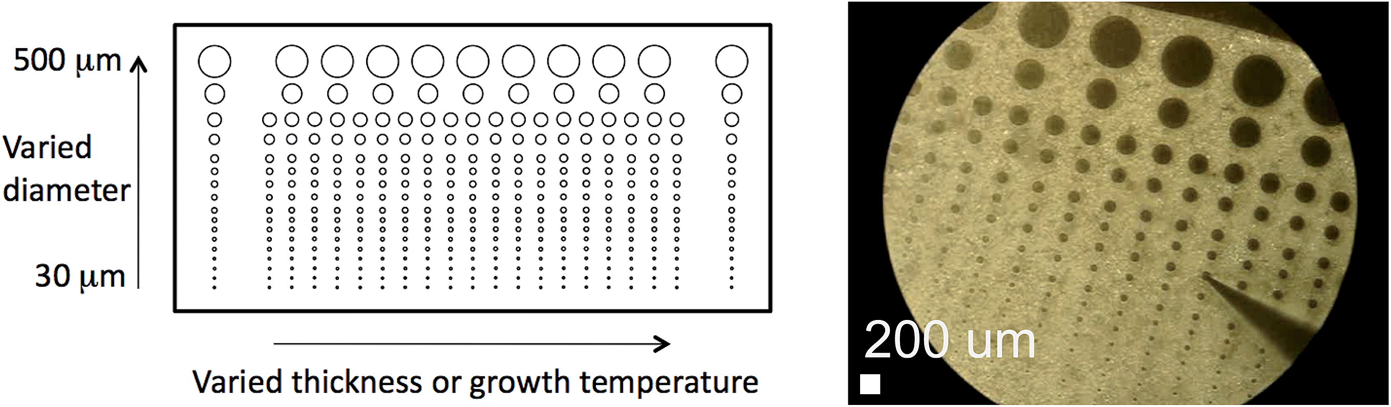 | ||
| Fig. 2 Layout of a library of (La0.8Sr0.2)0.95MnO3+δ thin film microelectrodes grown on a 5 × 10 mm substrate. Left: Schematic. Right: Optical microscope image of Library 1 during impedance testing. | ||
In preparation for impedance measurements, each substrate was adhered to a ∼10 × 20 × 0.6 mm alumina sheet using silver paste (DAD-87, Shanghai Research Institute). Heat treatment in a quartz tube under stagnant air at 600–700 °C for 1 h converted the paste into a porous counter electrode. Thus prepared, each library was installed in the automated impedance microprobe and heated to a stage temperature of 750 °C, resulting in a temperature of 735 °C at the microelectrodes due to the temperature gradient across the YSZ substrate. When a particular microelectrode was contacted by the probe tip, its average temperature decreased further (due to cooling by the probe tip) to ∼710 °C, with the exact value depending on the microelectrode diameter. A detailed discussion of the temperature calibration is given in the ESI.† The oxygen partial pressure (pO2) in the chamber was varied over the range 10−3 to 1 bar by flowing bottled oxygen or oxygen–nitrogen mixtures through the chamber and then past a zirconia-based oxygen sensor (Setnag) housed in a quartz tube in a separate furnace. The pO2 was allowed to stabilize at each condition prior to the acquisition of impedance data; typical stabilization times were 0.5–3 h. The total pressure in the chamber was always 1 bar. The microelectrodes were contacted using a probe tip made of Paliney7, a commercial alloy containing 35% Pd, 30% Ag, 14% Cu, 10% Au, 10% Pt, 1% Zn (American Probe & Technologies, 20 μm tip radius). Several measurements were repeated using a probe tip made of Pt0.7Ir0.3 (Moser, 10 μm tip radius); identical results were obtained. The former probe material was preferred because it did not scratch the microelectrodes and thus enabled multiple measurements over the range of conditions of interest. Uncertainty in the tip position, the sources of which are discussed in the ESI,† precluded reliable measurement of microelectrodes less than 100 μm in diameter. The use of silver as a counter electrode creates a contamination concern, and indeed, in other, longer term studies, it was observed that silver can migrate from the back of the electrolyte substrate to the microelectrode surface. In the present work, the contamination concern was mitigated by completing the measurement of each library in two days or less. To confirm the adequacy of this approach, some impedance spectra were collected under identical conditions at both the beginning and the end of the study (for Library 2 and the supplemental library); the resulting spectra were found to be nearly identical.
Impedance spectra were acquired using a frequency response analyzer (Solartron Modulab) with an applied a.c. voltage of 30 mV, no applied d.c. bias, and a typical frequency range of 10 kHz to 32 mHz. As described in the ESI,† cooling of the sample by the probe tip generated a 10–50 °C temperature drop between the top (measurement) and bottom (counter) electrodes, detected in the form of a 5–25 mV Seebeck voltage (with the exact value depending on the microelectrode diameter (Fig. S4†)). Consequently, each impedance spectrum was effectively measured under 5–25 mV anodic d.c. bias (with oxygen ions being driven from the electrolyte into the microelectrode). Selected measurements were repeated with an applied a.c. voltage of only 10 mV, and identical results were obtained, indicating that all measurements remained in the linear regime and thus that the Seebeck voltage had negligible impact on the electrochemical response. The analyzer calibration was verified in advance by acquiring impedance spectra from test circuits containing precision megaohm resistors and nanofarad capacitors; fits to these spectra reproduced the expected resistance and capacitance values with <3% error. Impedance spectra acquired from the LSM microelectrodes were fit by an expression similar to that first proposed by Fleig et al.,6 as described in detail below.
Morphological features were reexamined after impedance measurements. The sample surfaces were coated with a conductive layer of ∼10 nm carbon (Cressington 108) and/or ∼10 nm osmium and then characterized by scanning electron microscopy (SEM, Zeiss 1550 VP). Additionally, cross-sections of selected regions were prepared and imaged using focused ion beam (FIB) milling and SEM (FEI Helios Nanolab 600) after application of a protective layer of several hundred nm platinum.
3. Results of physical characterization
X-ray diffraction patterns acquired prior to patterning are shown in Fig. 3 (for Libraries 1 and 2) and Fig. S5† (for the supplemental library). The patterns from the thickness libraries (Library 1 and supplemental) exhibit reflections that correspond primarily to (110)-oriented grains. Some intensity from (012) and (202) reflections is also evident. The graded thickness of these libraries was visible by optical microscopy, with thinner regions giving rise to a lighter color (Fig. 2). The patterns from the growth temperature library, Library 2, show no reflections at growth temperatures of ∼580 °C and below, indicating those regions of the film were largely amorphous and/or had grains too small to yield sharp diffraction peaks with intensity above the background. At growth temperatures of ∼615 °C and higher, the films appeared crystalline with similar orientations as measured from the thickness library and an out-of-plane (110) spacing that decreased slightly with increasing growth temperature (Fig. S6†). A transition from XRD-amorphous to crystalline growth has been observed over a similar range of growth temperatures for La0.6Sr0.4CoO3−δ (ref. 22) and La0.58Sr0.4Co0.2Fe0.8O3−δ.23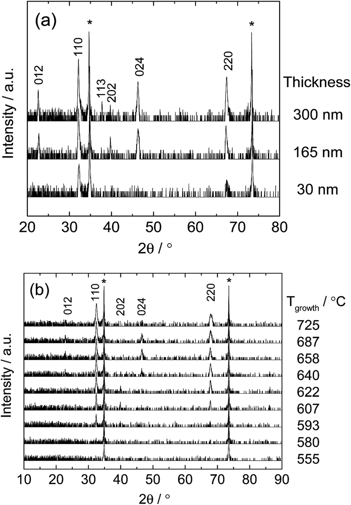 | ||
| Fig. 3 X-ray diffraction patterns acquired from various regions of (a) Library 1, and (b) Library 2 (Table 1). The Miller indices of each LSM reflection are indicated. Reflections marked with an asterisk are from the YSZ substrate. | ||
Rocking curves obtained from Library 2 revealed profiles about the (110) diffraction intensity that were best fit using two Voigt peaks, yielding two sets of values for the full width at half maximum (FWHM, Fig. S7†). The FWHM of the sharper component remained constant with growth temperature, whereas that of the broader component decreased, suggesting that the films had a thin, near-perfect epitaxial layer adjacent to the substrate overlaid with a thicker, slightly misoriented layer.24 Cross-sectional FIB-SEM images acquired after impedance measurements indicated that the films were dense. A representative image is shown in Fig. 4. It can be presumed that the films were also dense as grown. Optical profilometry and FIB-SEM images confirmed the film thickness was uniform across Library 2, and the film color appeared uniform across that library (not shown), consistent with a uniform thickness. The surface roughness was 1–2 nm RMS throughout (Fig. S6†). The SIMS measurement (Fig. S8†) indicated the cation concentrations were uniform through the bulk of the film.
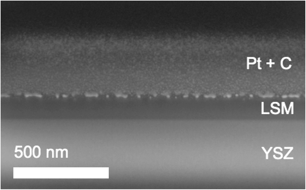 | ||
| Fig. 4 FIB-SEM cross-section acquired from Library 2 after impedance measurements. The sample was coated with conductive and protective layers of carbon and platinum prior to FIB milling to facilitate imaging. The top surface is tilted 52° away from the viewer. | ||
AFM micrographs collected after patterning but before electrochemical characterization are shown in Fig. 5 (Library 1), Fig. 6 (Library 2), and Fig. S9† (supplemental library). These images are indistinguishable from corresponding images that were collected before patterning (not shown). The features are interpreted as corresponding to grains resulting from columnar growth.25 The grain size is seen to increase with increasing thickness (Fig. 5 and S9†) or increasing growth temperature (Fig. 6 and S10†), and nanometer-sized grains are apparent for all films. Such growth characteristics are again typical. Quantification of these trends by image analysis (Fig. S11†) revealed a largely monotonic variation in grain boundary density across the thickness library, spanning from 45 to 95 μm μm−2 (Fig. 7a). For the growth temperature library, the range was wider, spanning from 10 to 100 μm μm−2 (Fig. 7b). Importantly, SEM micrographs acquired after impedance testing indicate that these grain size differences persisted through the two days of high-temperature exposure at 735 °C (Fig. S10†). In short, the thickness libraries and growth temperature library prepared in this work were also effectively “grain size libraries” with grain sizes that remained stable during the electrochemical impedance measurements.
 | ||
| Fig. 5 Atomic force micrographs of selected microelectrodes from Library 1 acquired after patterning. The corresponding thickness and root-mean-squared roughness values are listed below each image. | ||
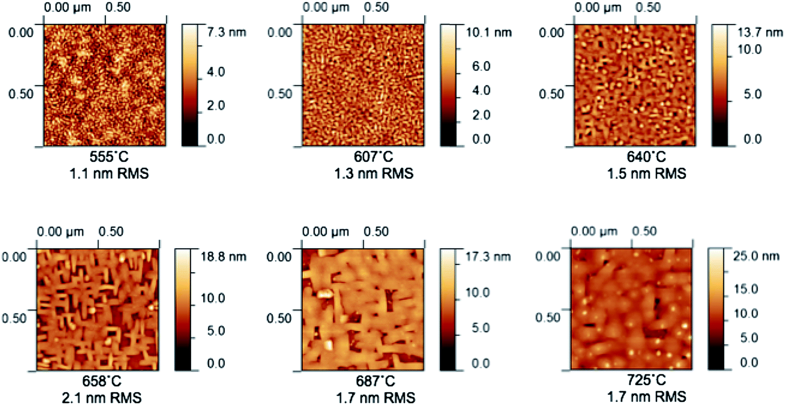 | ||
| Fig. 6 Atomic force micrographs of selected microelectrodes from Library 2 acquired after patterning. The corresponding growth temperature and root-mean-squared roughness values are listed below each image. | ||
 | ||
| Fig. 7 Exposed grain boundary length per unit surface area, estimated using AFM images from microelectrodes in (a) Library 1, and (b) Library 2. | ||
4. Results of electrochemical characterization
Before presenting electrochemical impedance results, it is valuable to consider the nature of the system under investigation and the likely reaction pathway. Consistent with what has been previously suggested in the literature, it is posited here that the dominant pathway proceeds as shown in Fig. 8: oxygen gas reacts with electrons over the entire surface of the LSM microelectrode; electrons arrive at the reaction sites by traveling laterally through the LSM from the probe tip; and the oxygen ions created in the reduction reaction are incorporated into and migrate through the mixed conducting LSM film and then into the YSZ electrolyte.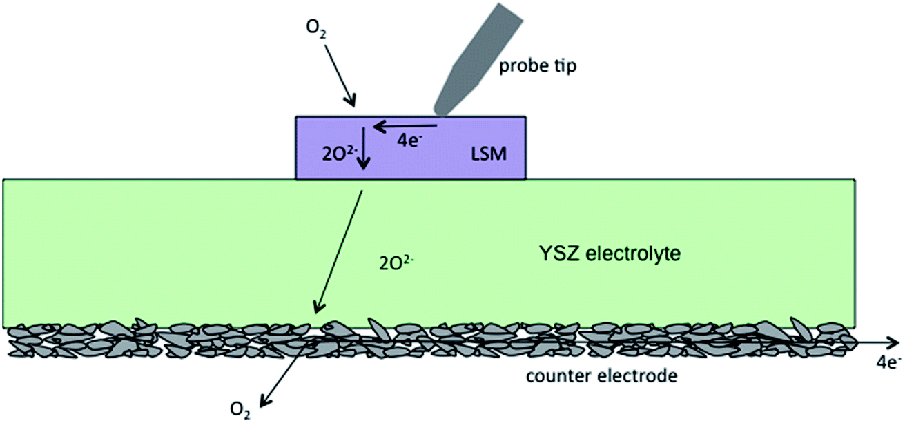 | ||
| Fig. 8 Schematic of the posited through-film reaction pathway. | ||
A model for this sequence of steps, producing the result shown in Fig. 9, can be postulated by first treating transport through the LSM. It has been shown elsewhere that the electrochemical impedance response arising from 1D diffusion through a generic mixed ionic and electronic conductor (MIEC) can be rigorously mapped to an equivalent circuit based on a generalized transmission model.26,27 Under the condition of electroneutrality, this generic MIEC equivalent circuit reduces (as also shown previously) to an electronic path in parallel with an ionic path, with the paths linked via what is termed the chemical capacitance. In the case of LSM, the high electronic conductivity suggests the resistance along the electronic path (in the through-plane direction) is negligible. Accordingly, it is omitted from the circuit in the present analysis. The termination of the MIEC circuit at the LSM/gas/probe interface is assumed here to be reversible to electrons but to display a finite electrochemical reaction resistance with respect to incorporation/release of oxygen ions. This reaction is further taken to be associated with a surface ionic capacitance term. The buried LSM/YSZ interface is assumed here to be reversible to ions and blocking to electrons, and thus is modeled by a simple (double-layer) electronic capacitance. To describe the entire cell, this MIEC system is placed in series with a single resistor that accounts for bulk ion diffusion through the YSZ electrolyte as well as any lateral electron migration resistance (sheet resistance) from the probe tip to the surface reaction sites. Finally, as is common in impedance spectroscopy, dispersion effects are captured here by replacing (selected) ideal capacitors by a constant phase element (CPE) with impedance ZCPE = Q−1(jω)−n, where Q is a constant,  , ω is the frequency of the applied a.c. signal, and n is a constant between 0 and 1.28 Specifically, it was observed during data analysis that such a substitution for the ionic surface capacitance significantly improved the quality of the fits, so this substitution was implemented throughout.
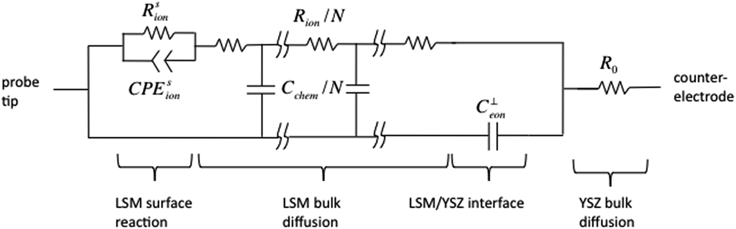 | ||
| Fig. 9 Equivalent circuit corresponding to the reaction pathway shown in Fig. 8. | ||
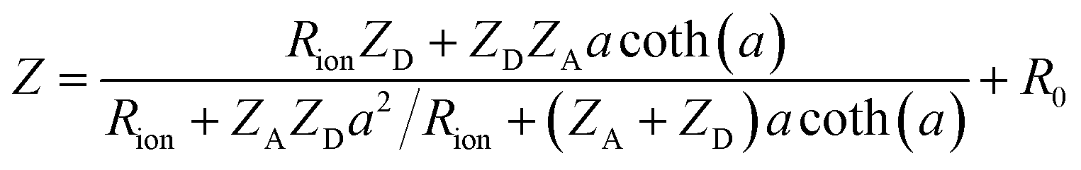
The complex impedance of the resulting equivalent circuit (with analytical derivation provided in the ESI†) is:
 | (1) |
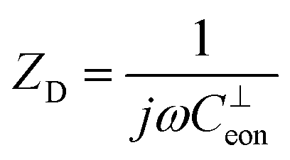 ,
,  , and
, and  . The seven fit parameters in this model are Rsion, Ysion, n, Rion, Cchem, Ceon, and R0, which correspond, respectively, to the LSM surface reaction resistance, the LSM surface ionic capacitance (in the form of a constant phase element magnitude and exponent), the LSM through-film oxygen ion diffusion resistance, the LSM chemical capacitance, the LSM/YSZ interfacial electronic capacitance, and the sum of the YSZ oxygen ion diffusion resistance and the small LSM electronic sheet resistance. This result is virtually identical to that presented in brief previously by Fleig et al.,6 except in the use of CPEs. In that earlier work, a CPE was employed to describe the interfacial electronic capacitance, whereas in the present study a CPE was used to describe the surface ionic capacitance, as noted above. The fits were performed using a complex nonlinear least squares fitting routine implemented in a custom Matlab code. The residual of each complex impedance datum was weighted by the complex modulus of the datum, which is commonly used as a proxy for the variance of that datum.28 To validate the routine, impedance spectra from validation samples were fit to relevant equivalent circuits using both this custom code and a commercial code (Zview), with identical results obtained. From the CPE fit parameters, the effective surface ionic capacitance Csion was calculated using the standard expression Csion = (Ysion)1/n(Rsion)(1/n)−1.28
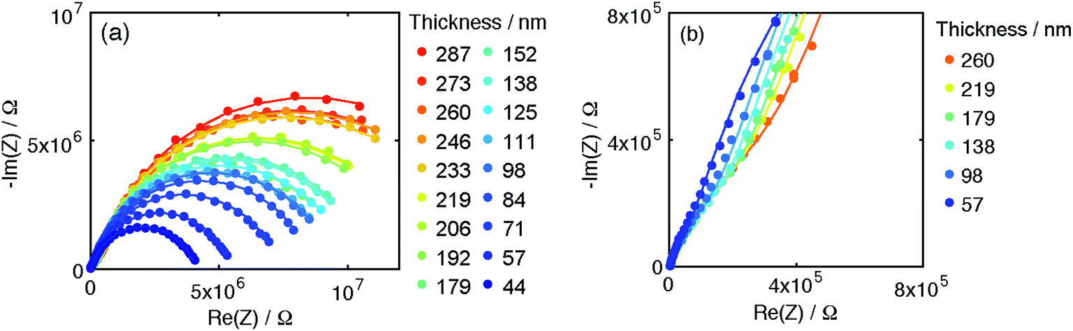
Selected raw impedance spectra and the corresponding fit curves from a microelectrode in Library 1 (200 μm diameter, 192 nm thick), are shown in Fig. 10 for a representative measurement at two different oxygen partial pressures (T ∼ 710 °C). As presented in the complex plane, Fig. 10a, the spectra are formed of a large arc at lower frequencies, an additional smaller feature at higher frequencies, and a relatively small offset from the origin along the real direction appearing at the high frequency limit. These spectral features are similar to those observed by Fleig et al.,6 and they are broadly akin to the spectra observed in other reports as well.7–9 Significantly, the features are precisely captured by the proposed model, as indicated by the correspondence between the measured and fit spectra. The quality of the fits is particularly evident in the magnitude and phase plots shown in Fig. 10d and e, respectively. The model parameters extracted from these fits are listed in Table 2 along with 95% confidence intervals. While (as is widely appreciated) an excellent fit with reasonably small confidence intervals does not, alone, validate a model, it does give confidence in the approach.
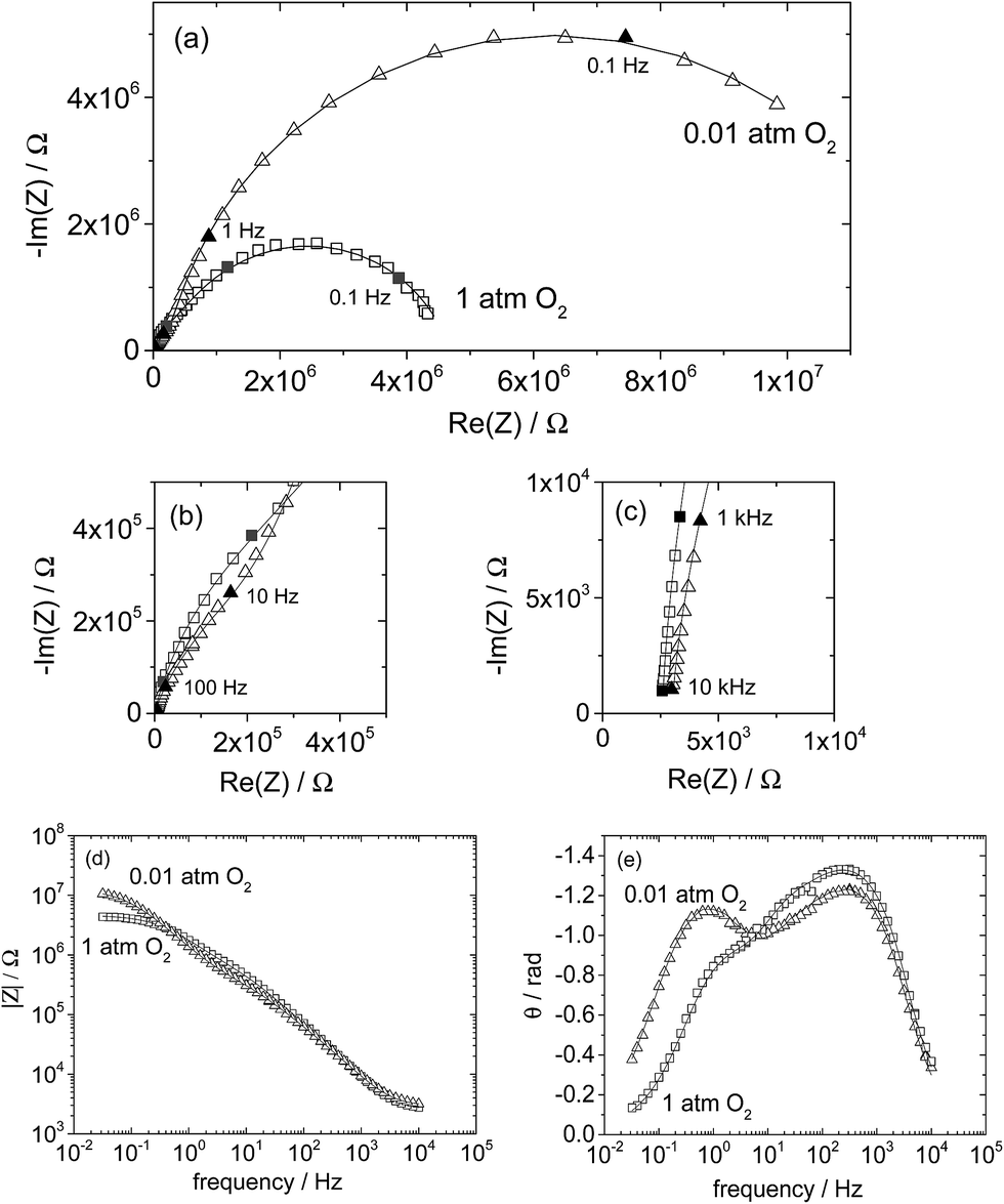 | ||
| Fig. 10 Representative impedance spectra acquired from (La0.8Sr0.2)0.95MnO3+δ microelectrodes (Library 1, 200 μm diameter, 192 nm thickness, T ∼ 710 °C) under 1 bar O2 (square markers) or 0.01 bar O2 (triangles): (a–c) Nyquist plots at various scales, (d) magnitude plot, and (e) phase plot. Curves are fits to the data according to eqn (1). | ||
| Parameter | 1 bar O2 | 0.01 bar O2 |
|---|---|---|
| R sion/106 Ω | 3.47 ± 0.09 | 10.18 ± 0.21 |
| R ion/106 Ω | 1.09 ± 0.07 | 0.55 ± 0.08 |
| R 0/103 Ω | 2.63 ± 0.02 | 3.03 ± 0.04 |
| Y sion/10−8 F s(n−1) | 7.34 ± 0.02 | 7.43 ± 0.06 |
| n | 0.76 ± 0.01 | 0.77 ± 0.02 |
| C chem/10−8 F | 2.71 ± 0.02 | 4.34 ± 0.07 |
| C eon/10−8 F | 1.65 ± 0.01 | 1.52 ± 0.02 |
The data in Table 2 exemplify three findings that were observed for all microelectrodes in this work: (1) the surface resistance was always larger than the through-film diffusion resistance, but not by so much that the through-film resistance could be neglected; (2) the low frequency arc was consistently depressed, with the exponent parameter n (not shown) taking a value in all cases around 0.7–0.8; and (3) in any given measurement, the three capacitance values were within an order of magnitude of each other. One consequence of these characteristics is that the surface and through-film processes often displayed similar characteristic frequencies, particularly at high oxygen partial pressure, behavior also noted by Fleig.6 To avoid overfitting and the introduction of statistically insignificant quantities as a result of insensitivity to model parameters, when fitting the spectra acquired under 0.2 or 1 bar O2, the value of Rion was sometimes fixed at a physically sensible value, as detailed below.
We now evaluate the influence of microelectrode diameter on impedance response, using data from Library 1 to illustrate the trends observed. Selected spectra from microelectrodes with diameter ranging from 102 to 512 μm and a fixed thickness of 246 nm are presented in Fig. 11, and the six model parameters extracted from these and other spectra are presented as a function of diameter in Fig. 12.
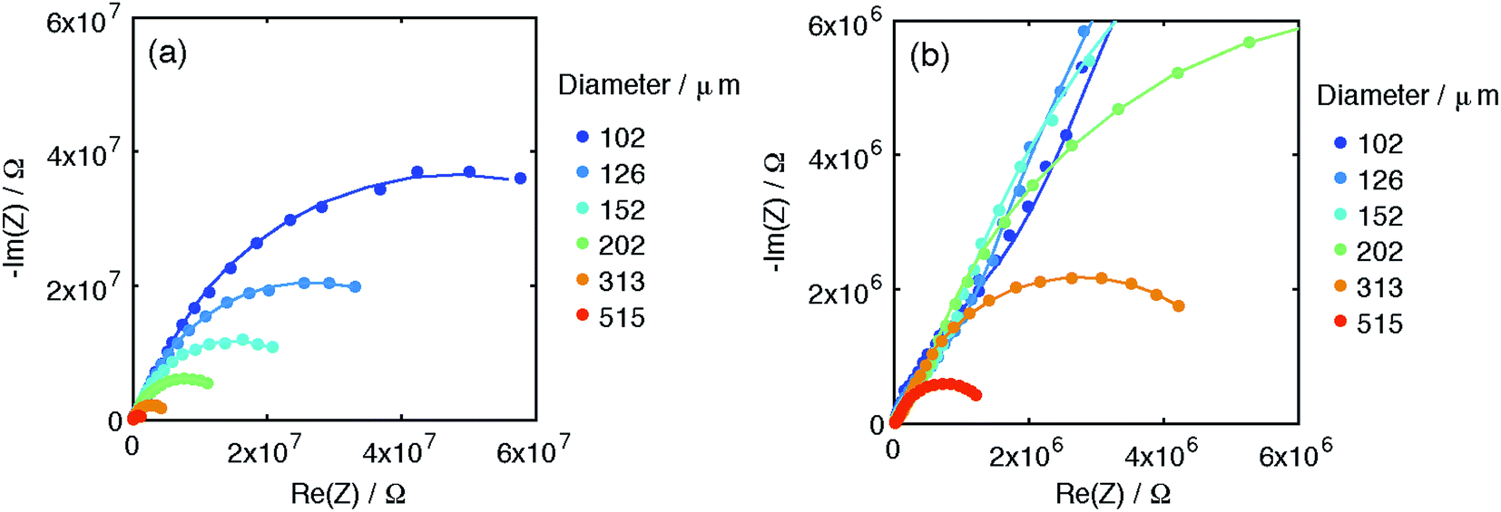 | ||
| Fig. 11 Diameter dependence of impedance spectra of 246 nm thick microelectrodes of Library 1 under 0.01 bar O2 (T ∼ 710 °C). (a and b) Nyquist plots at two different scales. Curves are fits to the data according to eqn (1). | ||
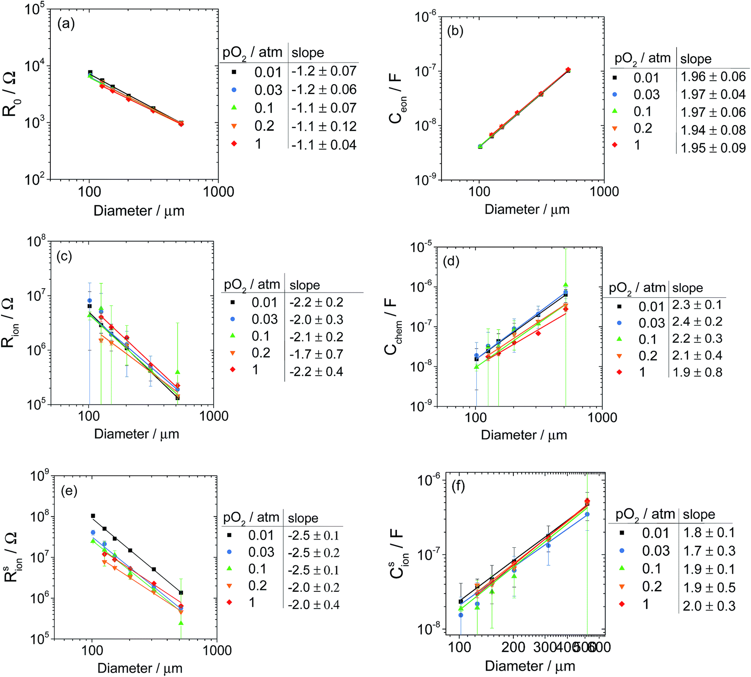 | ||
| Fig. 12 Diameter dependence of six parameters obtained from fits to impedance spectra from 246 nm thick microelectrodes in Library 1 under various oxygen partial pressures as indicated (T ∼ 710 °C): (a) surface reaction resistance; (b) surface ionic capacitance; (c) bulk ionic resistance; (d) bulk chemical capacitance; (e) offset resistance; and (f) interfacial electronic capacitance. 95% confidence intervals from the impedance analysis are shown, except where they are smaller than the markers. Lines shown are linear fits to the values shown weighted by the inverse of the corresponding variance obtained from the impedance analysis. Slopes (and 95% confidence intervals) of the lines are indicated in the legends. | ||
Considering first the parameter R0, Fig. 12a shows that this resistance scales approximately linearly with the inverse of the microelectrode diameter. In the limit of R0 being dominated by the resistance of an infinitely thick electrolyte (with minimal contribution from electronic sheet resistance), its value is given by the Newman equation, expressed as R0 = 1/(2dσYSZ), where d is the microelectrode diameter and σYSZ is the conductivity of the Y0.15Zr1.85O1.93 electrolyte.29 This relationship indicates that a slope of −1, similar to that observed, is expected in the double-logarithmic plot. In the present case, however, the electrolyte thickness is only a few times larger than that of the microelectrode diameter. Considering the analytical correction appropriate when the conductor is thick but finite,29 and recognizing that deviations from the ideal expression increase with increasing microelectrode diameter, a slope of magnitude slightly greater than 1 is expected, consistent with the experimental observation. Using the R0 values from the smallest microelectrodes, the Newman relationship implies an ionic conductivity of the electrolyte in the range from 0.006 to 0.008 S cm−1, in reasonable agreement with the reported value at ∼710 °C of 0.015 S cm−1.30 The parameter R0 is also seen to be insensitive to pO2, consistent with the electrolytic behavior of YSZ. Additional contributions to the deviation of the slope in Fig. 12a from −1 are attributed to tip cooling, as discussed in the ESI.† In brief, the thermally grounded tip draws heat from the microelectrodes, with greater impact on microelectrode average temperature the smaller the diameter. Moreover, evolution of the tip geometry towards a more blunt contact with time likely rendered the tip cooling effect more pronounced for the later, low pO2 measurements, for which the deviation from −1 of the slope in the double-logarithmic plot is greater. The temperature of ∼710 °C reported throughout this work corresponds to the actual average temperature of a 200 μm diameter microelectrode during measurement, after tip cooling is taken into account. Finally, although R0 is 3 to 4 orders of magnitude smaller than the other two resistances, since R0 is the high frequency offset and there are numerous data points near this offset, model sensitivity to this parameter is high and the confidence intervals are small.
Turning to the other two resistances, Rsion is about an order of magnitude greater than Rion, and it is apparent that when Rsion is large, which occurs at low pO2, resolution of these two quantities improves and the uncertainty intervals for both (and especially for Rion) decrease. In the case of Rion, a slope of −2 is expected if this term accurately represents the ionic resistance of the LSM microelectrodes. The measured slopes range from −1.7 to −2.2, close to the expected value. The term Rsion, representing the surface electrochemical reaction resistance, displays a slope between −2.0 and −2.5, identical to the range reported by Fleig.6 That this slope is close to −2 supports the hypothesis that the electrochemical reaction occurs over the entire surface of the LSM electrode. The deviation from −2 is attributed to the tip cooling and tip blunting effects described above and detailed in the ESI.† Consistent with this attribution, the deviation from the ideal slope is greatest at low pO2, which corresponds to the later measurements and thus a blunter tip with slightly increased cooling. Ignoring this experimental challenge, from the perspective of the overall physical process, the observed scaling laws imply that Rion and Rsion are justifiably reported in terms of area normalized quantities, hereafter designated as ![[R with combining tilde]](https://www.rsc.org/images/entities/i_char_0052_0303.gif) (and reported in units of Ω cm2).
(and reported in units of Ω cm2).
These quantities can be used to assess a posteriori the validity of the model assumption that the counterelectrode impedance is negligible. Using conservative values for the relevant quantities (reaction rate constant k = sion−1 = 0.001 S cm−2, electrolyte conductivity σ = 0.006 S cm−1, electrolyte thickness t = 0.05 cm, and microelectrode radius r = 0.025 cm), the effective counterelectrode radius given by eqn (13) in Sasaki et al.31 is found to be 1.11 cm. This large value indicates that in practice the entire counterelectrode area (0.5 cm2) experiences current flow. Considering a circle of equivalent area for ease of calculation, the effective counterelectrode radius can be taken to be 0.4 cm. Using this value, an estimate for the extent of isolation (i.e., the percentage of the total measured impedance that can be assigned to the microelectrode) can then be calculated from eqn (14)31 to be 99.6%. This result conservatively assumes that the counterelectrode and microelectrode have the same sion, but in separate experiments on symmetric cells, sion for a comparable silver paste electrode was measured to be 1–2 orders of magnitude smaller than assumed here, thus increasing the extent of isolation. In short, the counterelectrode impedance can safely be neglected.
The three capacitance parameters are seen in Fig. 12 to scale with the square of diameter, again consistent with the electrochemical pathway posited above in which surface exchange and through-film transport occur over the entire LSM area. A pathway in which the rate-limiting step occurs at the three-phase boundary at the edge of the LSM (where the LSM, YSZ, and gas phases intersect) would be expected to generate different scaling behavior.
Of the three capacitance terms, Ceon, which represents the termination of the electronic rail at the LSM|YSZ interface, is the smallest by about a factor of three relative to the other two terms, and the uncertainty in this parameter is also the smallest (for reasons similar to those described above for the parameter R0). In principle, this double-layer capacitance should be determined by a screening length that, in turn, depends on the sum of the bulk concentrations of all charged defect species for which the interface is blocking.32 The data in Fig. 12b show Ceon to be entirely independent of pO2, suggesting that, in these (La0.8Sr0.2)0.95MnO3+δ films, the concentrations of the blocked defects are constant. Based on studies of a similar composition, La0.8Sr0.2MnO3+δ33 it can be expected that (La0.8Sr0.2)0.95MnO3+δ has a slight excess of oxygen (δ ≳ 0) at 710 °C and over the range 10-2 to 1 bar O2. Despite this excess, the electron hole concentration (presumably the relevant blocked defects) is largely independent of pO2,33-36 consistent with the pO2-independent behavior of Ceon observed here. The slope of 2 observed in the double-logarithmic plot of Ceonvs. diameter reveals that this quantity is correctly assigned as being proportional to area. Accepting that the slope deviation from −1 in the case of R0 is, in part, a result of tip cooling, the rather precise slope of 2 observed in Fig. 12b indicates that tip cooling does not affect Ceon, in turn, suggesting that its associated carrier concentrations are insensitive to temperature in the range 710–800 °C. This suggestion is supported by measurements performed at ∼800 °C using the supplemental library (not shown), which gave virtually identical values of Ceon to those reported here for Library 1 at ∼710 °C.
The second capacitance term Csion, which represents the termination of the ionic rail at the LSM|gas interface, is like Ceon, largely independent of pO2. If Csion is correlated primarily to the oxygen vacancy concentration, its insensitivity to pO2 is not surprising; in the oxygen excess regime, the oxygen vacancy concentration is, as already noted, small and changes only slightly with pO2,36 as stoichiometry changes are accommodated via the creation of cation vacancies.33 The slopes in the double-logarithmic plot of Csionvs. electrode diameter deviate slightly downwards from 2, but the confidence intervals are wide enough to suggest caution in assigning significance to this deviation. The third capacitance term, Cchem, which reflects the redox behavior of the LSM bulk, displays a slight dependence on pO2, and in the double-logarithmic plot, the deviation of the slope from 2 is more substantial than in the case of Csion. Nevertheless, the scaling observed with diameter indicates that for all three capacitance terms, the properties are justifiably reported in terms of area-normalized quantities, hereafter designated as ![[C with combining tilde]](https://www.rsc.org/images/entities/i_char_0043_0303.gif) (and reported in units of F cm−2).
(and reported in units of F cm−2).
Turning now to the thickness dependence of the electrochemical behavior, raw impedance spectra and fits from microelectrodes with 200 μm diameter from Library 1 at pO2 = 0.01 bar are shown in Fig. 13. The spectra correspond to 18 different microelectrode thicknesses spanning 44 to 287 nm, a large number that underscores the power of the parallel fabrication and automated testing approach. The spectra reveal that the overall impedance grows monotonically with increasing thickness, as broadly observed by previous workers.7–9 Significantly, the spectra are again well-represented by the model.
 | ||
| Fig. 13 Thickness dependence of impedance spectra of 200 μm diameter microdot electrodes from Library 1 under 0.01 bar O2 (T ∼ 710 °C). (a and b) Nyquist plots at two different scales. Curves are fits to the data according to eqn (1). | ||
The thickness dependence of the six parameters extracted from the data shown in Fig. 13 and other datasets collected at different values of oxygen partial pressure are summarized in Fig. 14. (Here the data are presented on linear rather than logarithmic scales, giving the appearance of larger uncertainty than in Fig. 11, but, in fact, the confidence intervals are comparable.) As alluded to above, in order to reduce the uncertainty in derived parameters (Fig. S12†) and render trends with thickness more readily apparent, the Rion values at 1 and 0.2 bar O2 were fixed at the average of the values determined under the other three atmospheric conditions, a step justified by the relative insensitivity of Rion to pO2, evident in both Fig. 12 and 14.
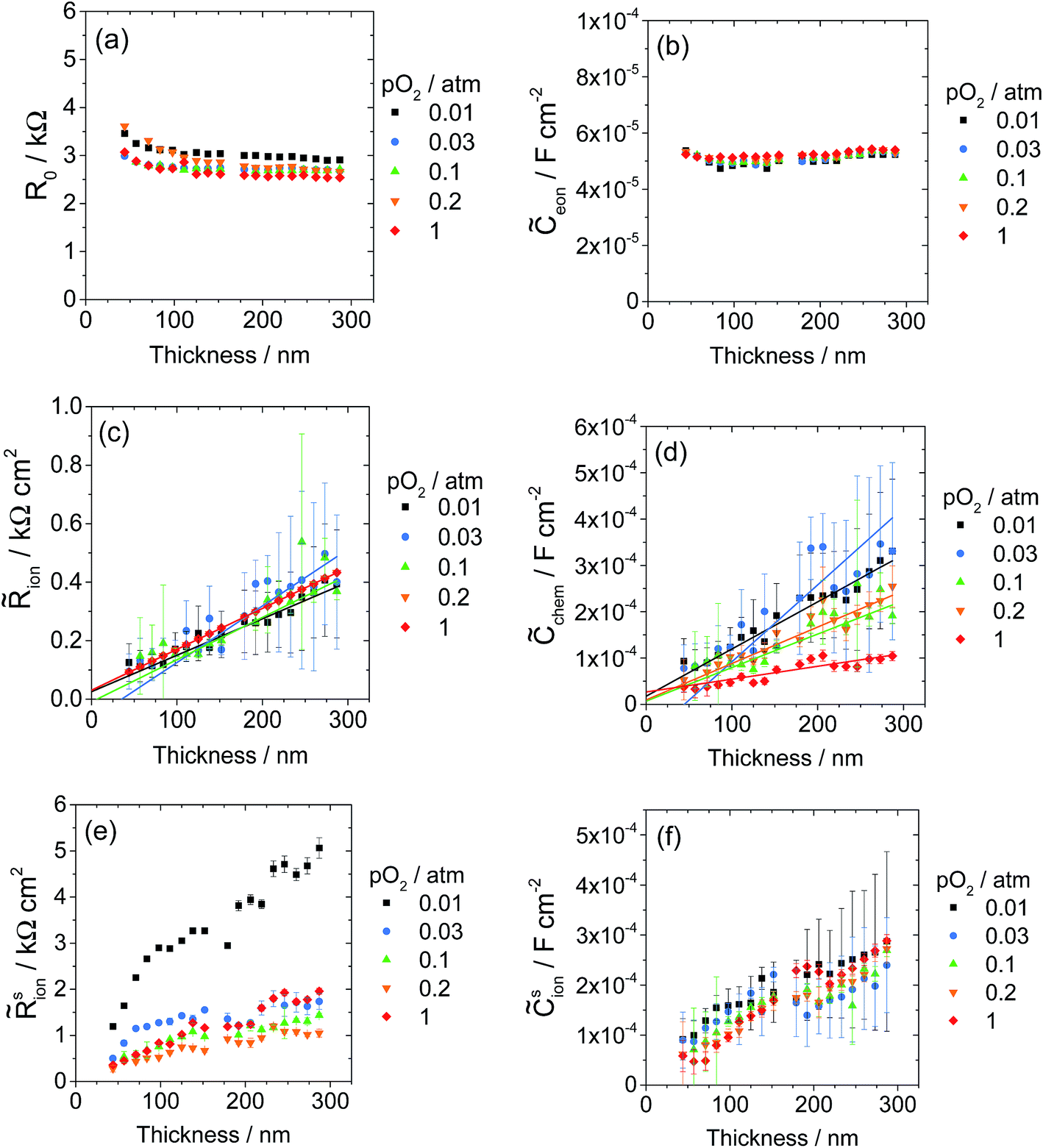 | ||
| Fig. 14 Thickness dependence of six parameters obtained from fits to impedance spectra from 200 μm diameter microelectrodes in Library 1 under various oxygen partial pressures as indicated (T ∼ 710 °C): (a) surface reaction resistance; (b) surface ionic capacitance; (c) bulk ionic resistance; (d) bulk chemical capacitance; (e) offset resistance; and (f) interfacial electronic capacitance. When fitting the impedance spectra acquired under 0.2 and 1 bar O2, Rion was fixed at the value determined by averaging the Rion values obtained from fits to impedance spectra acquired from the same microelectrode at 0.01, 0.03, and 0.1 bar O2. 95% confidence intervals are shown, except where they are smaller than the markers. Lines shown in (c) and (d) are linear fits to the values shown weighted by the inverse of the corresponding variances obtained from the impedance analysis. | ||
Beginning again with R0, shown in Fig. 14a, this parameter is largely independent of thickness and oxygen partial pressure, as expected for a term that corresponds primarily to the bulk ionic resistance in the YSZ substrate. However, R0 does increase slightly in the thinnest films, and this behavior is attributed to a small contribution from electronic sheet resistance. Wedig et al. have previously observed that sheet resistance can distort the results of thin film impedance measurements,37 but their calculations indicate that this distortion is only significant for much larger sheet resistances than observed in the present study. The cause of the slight increase in R0 with decreasing pO2 is not entirely known, but may be due to mechanical blunting of the tip, which, as noted above, may have slightly lowered the temperature of the low pO2 measurements. The capacitance term eon, shown in Fig. 14b, is independent of film thickness, consistent with the association of this property with the LSM/YSZ interface. The bulk parameters, ion and chem, scale linearly with thickness, as expected, although the trend-lines do not precisely pass through the origin. These values from Library 1 are discussed in more detail below alongside analogous values obtained from Library 2.
Considering next the LSM|gas surface terms, a striking dependence on film thickness is seen for both the surface reaction resistance sion, Fig. 14e, and the effective surface ionic capacitance sion, Fig. 14f. A key assumption in almost every study employing geometrically defined, patterned electrodes is that of a chemically and structurally reproduced surface with geometry-independent properties. Here, such an assumption is clearly found to be invalid. Not only does the behavior of the surface change, the growth of the total impedance with thickness (seen in Fig. 13) is, in fact, dominated by an increase in sion. This unexpected behavior of sion indicates that some critical feature of the surface changed with thickness. The microstructural evaluation of the film surface morphology points towards the grain structure as that critical factor. Specifically, the apparent negative correlation between the area density of exposed grain boundaries and the film thickness (Fig. 5 and 7) suggests that these grain boundaries are more active for oxygen electro-reduction than are the boundary-free surfaces.
The growth temperature library, Library 2, provides an excellent test for this hypothesis. As noted above, varying growth temperature resulted in a substantial variation in the area density of surface-terminating grain boundaries at fixed film thickness (Fig. 6, 7 and S10†), while the lattice constant and even film roughness remained relatively constant (Fig. S10†). Representative impedance spectra acquired from a series of microelectrodes in that library (d = 200 μm, t = 135 nm, T ∼ 710 °C, pO2 = 0.2 bar) are shown in Fig. 15. As with Library 1, each spectrum is comprised of a large arc at lower frequencies, a smaller second feature at higher frequencies, and a small high-frequency offset along the real axis.
 | ||
| Fig. 15 Growth temperature dependence of impedance spectra from 200 μm diameter microelectrodes in Library 2 under 0.01 bar O2 (T ∼ 710 °C), shown in the Nyquist representation. Points are raw data, curves are fits according to eqn (1). | ||
Parameters extracted from fits to these and other spectra are shown in Fig. 16. (In this case, because no particular scaling behavior is anticipated, either semi-log or linear plots are selected for presentation depending on convenience.) For this library, selected results obtained after one day of exposure at high temperatures are also presented; it is evident that there is little change in the material properties with time. It is also apparent that the statistical uncertainty in parameters derived from Library 2 are substantially smaller than those from Library 1, a result tentatively assigned to improved control algorithms in later measurements. The parameters R0 and eon, which correspond to the YSZ bulk and the YSZ|LSM interface, are found to be largely independent of growth temperature and of oxygen partial pressure during measurement. Moreover, the absolute values of R0 and eon, ∼2.8 kΩ and 50 μF cm−2, respectively, are almost identical to those found in Library 1 for microelectrodes of the same 200 μm diameter, giving confidence in the measurement configuration of the microprobe system.
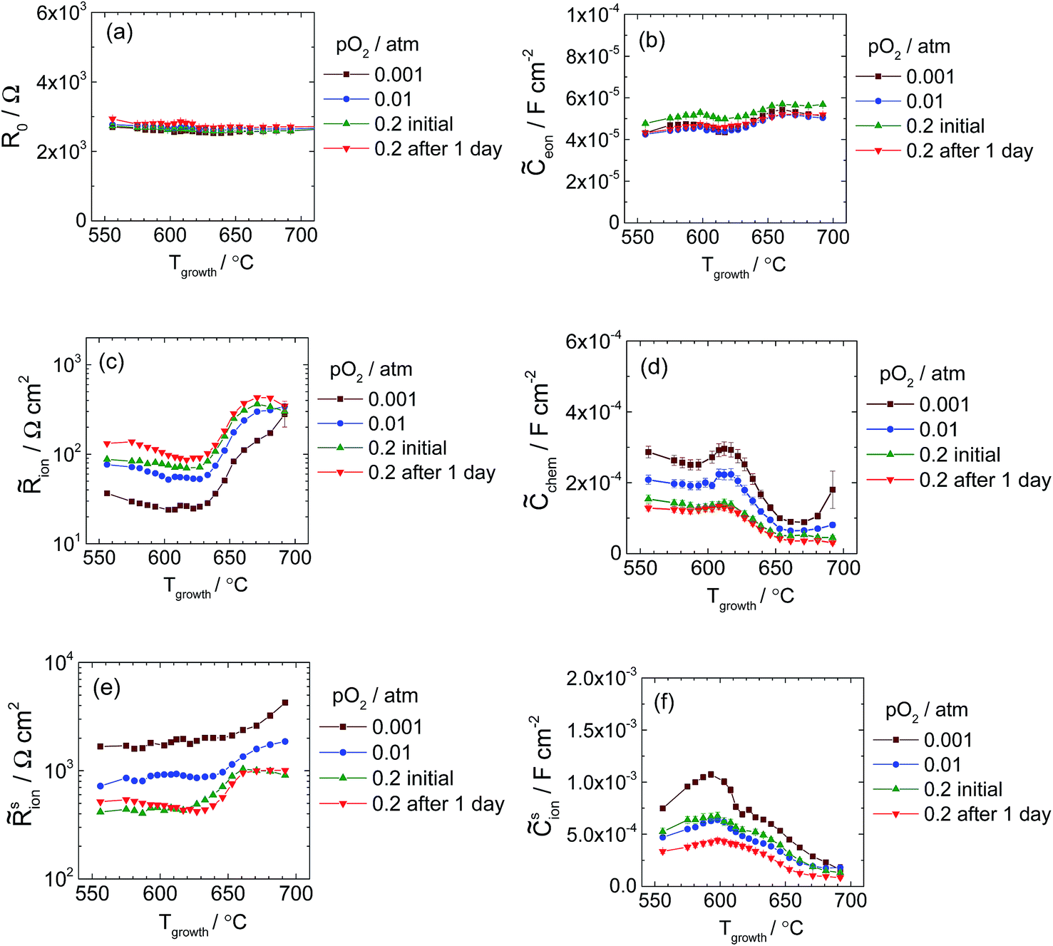 | ||
| Fig. 16 Growth temperature dependence of six parameters obtained from fits to impedance spectra acquired from 200 μm diameter microelectrodes in Library 2 under various oxygen partial pressures as indicated (T ∼ 710 °C): (a) offset resistance; (b) interfacial electronic capacitance; (c) bulk ionic resistance; (d) bulk chemical capacitance; (e) surface reaction resistance; and (f) surface ionic capacitance. 95% confidence intervals from the impedance analysis are shown, except where they are smaller than the data points. Lines connect the points as guides for the eye. | ||
Immediately evident from Fig. 16 is the significant and nonlinear impact of growth temperature on the remaining four properties of LSM microelectrodes. In particular, the surface exchange resistance sion, which was hypothesized to be influenced by the presence of surface-terminated grain boundaries, generally increases with increasing growth temperature, i.e., decreasing grain boundary density. Moreover, the changes in sion occur predominantly in the growth temperature range 630–680 °C, precisely the range in which the grain size increases most sharply (Fig. 6 and S8†). This correlation is explored quantitatively, for the specific case of 0.01 bar O2 and 200 μm diameter microelectrodes, by comparing the inverse of sion, which is a direct measure of surface activity, to the area density of exposed grain boundary length. The results, Fig. 17a, reveal that for each library, the surface activity scales linearly with the number density of grain boundaries. While the absolute values in sion between the two types of libraries differ, the linear scaling provides compelling evidence that the surface-terminating grain boundaries are the predominant active sites for oxygen electro-reduction (and oxygen evolution). From the slopes of these trends, it can be estimated that the surface activity of an LSM film increases by 10−13 Ω−1 per micron of added grain boundary length. The interpretation provided here is supported by two very recent 18O tracer diffusion studies of polycrystalline LSM films from which it was deduced that the surface exchange at grain boundaries was much greater than that at the grain-boundary free surface.11,38 In addition, an increase in the electrochemical reaction impedance in polycrystalline LSM films subjected to high temperature treatment has been attributed to grain growth and loss of the active surface-terminating grain boundaries.15
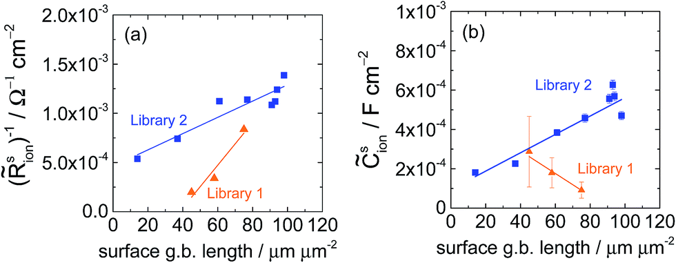 | ||
| Fig. 17 Dependence of surface electrochemical parameters on surface-terminated grain boundary length as measured from 200 μm diameter microelectrodes in Libraries 1 and 2 (varied thickness for Library 1 and varied growth temperature for Library 2) under 0.01 bar O2 (T ∼ 710 °C). (a) Electrochemical activity, defined as the inverse of the area-specific surface reaction resistance, and (b) area-normalized surface ionic capacitance. | ||
A myriad of reasons may be responsible for the difference in absolute magnitudes of sion obtained from the thickness and growth temperature libraries. Of these, that considered most likely is the possibility that the faster deposition (5 Hz frequency) of the growth temperature library may have generated a non-equilibrium surface, explicitly within the vicinity of the surface-terminating grain boundaries, with greater activity than that of the more slowly grown (1 Hz) thickness gradient libraries. The faster cooling rate employed upon completion of the growth may also have played a role, but given the high measurement temperature, quenching of the surface characteristics seems unlikely. The possibility that the use of different oxygen pressures during growth caused the observed electrochemical differences also is considered unlikely. Library 1 and the supplemental thickness library were grown under different oxygen pressures and yielded comparable results (Fig. S13†). Sample evolution over the long-time measurements is similarly deemed an unlikely explanation. As shown in Fig. 16 (for Library 2) and Fig. S13† (for the supplemental library), measurements performed immediately after library installation and those performed 1 to 2 days later gave essentially identical results. This electrochemical stability suggests negligible morphological changes during the measurements due to crystallization of any residual amorphous material present in the films grown at the lower temperatures.
A second unexplained difference in the two libraries lies in the dependence of sion on the presence of surface-terminating grain boundaries, Fig. 17b. In the thickness library, fewer grain boundaries (i.e., increasing film thickness) correlated with a larger sion, whereas in the growth temperature library, fewer grain boundaries (i.e., increasing growth temperature) coincide with a smaller sion. Thus, sion and sion are counter-correlated in Library 1, but correlated in Library 2. This intriguing result awaits further in-depth inquiry.
The variation of ion and chem with growth temperature may also ultimately be due to the impact of grain boundaries. ion tends to increase with increasing growth temperature and hence decreasing area-density of grain boundary length, which may plausibly be a result of enhanced oxygen ion conductivity along grain boundaries. This suggestion is consistent with oxygen tracer diffusion studies indicating that oxygen transport is substantially faster along the grain boundaries of LSM than through the bulk.11,38,39 In contrast to ion, chem tends to decrease with increasing area density of grain boundary length. This trend may reflect a lower capacity for oxygen stoichiometry changes in the grain boundary regions relative to the bulk. Trends in bulk properties with grain boundary density are further detailed in Fig. S14.† It should be noted that if transport is indeed dominated by grain boundaries, then the assumption of 1D transport through a homogenous material is, in principle, violated, particularly because the grain size varies through the thickness of the film, and the boundaries are slightly tilted. However, from the variation in grain boundary density, Fig. 7, the tilt angle is calculated to be <5° on average, and even for the thickest films, the density of grain boundaries changes with thickness by only no more than a factor of 2. Hence, violations to the model assumptions are small.
From the respective values of ion and chem the through-film ionic conductivity σion and the volume-normalized chemical capacitance ![[small epsilon, Greek, circumflex]](https://www.rsc.org/images/entities/i_char_e107.gif) chem can be readily computed using the expressions σion = L/ion, chem = chem/L, where L is the microelectrode thickness. Here we introduce the symbol chem to denote the volume-normalized chemical capacitance, in analogy with εdielec the volume-normalized dielectric capacitance (also recognized as the absolute permittivity), using a to indicate the atypical dimension of capacitance per unit volume. From these quantities it is then possible to compute the ambipolar diffusivity using the expression Dchem = L2/(ionchem) = σion/chem.26 For Library 1, the calculation was performed for each measurement and, upon observing only a weak dependence on thickness, for ease of comparison the values at each pO2 were averaged over all 18 thicknesses measured. (As stated previously, for the two highest pO2 conditions, at which ion could not be resolved, σion was taken to be the average of those values obtained at the other pO2 conditions.) For Library 2, the calculation was performed for three selected growth temperatures: the lowest and highest temperatures examined (556 and 692 °C, respectively), and 653 °C, which corresponds to the growth temperature used in the preparation of Library 1.
chem can be readily computed using the expressions σion = L/ion, chem = chem/L, where L is the microelectrode thickness. Here we introduce the symbol chem to denote the volume-normalized chemical capacitance, in analogy with εdielec the volume-normalized dielectric capacitance (also recognized as the absolute permittivity), using a to indicate the atypical dimension of capacitance per unit volume. From these quantities it is then possible to compute the ambipolar diffusivity using the expression Dchem = L2/(ionchem) = σion/chem.26 For Library 1, the calculation was performed for each measurement and, upon observing only a weak dependence on thickness, for ease of comparison the values at each pO2 were averaged over all 18 thicknesses measured. (As stated previously, for the two highest pO2 conditions, at which ion could not be resolved, σion was taken to be the average of those values obtained at the other pO2 conditions.) For Library 2, the calculation was performed for three selected growth temperatures: the lowest and highest temperatures examined (556 and 692 °C, respectively), and 653 °C, which corresponds to the growth temperature used in the preparation of Library 1.
The resulting values of σion, chem, and Dchem are shown in Fig. 18 along with comparable literature values. The ionic conductivity, Fig. 18a, is similar to the values measured using a d.c. blocking electrode method by Huang et al.40 from 2 μm thick sputtered La0.85Sr0.15MnO3+δ films, and nearly identical values were obtained by Fleig et al. from 100–250 nm thick (La0.8Sr0.2)0.92MnO3+δ films at ∼800 °C.6 The volume-normalized chemical capacitance, Fig. 18b, also agrees with the results for (La0.8Sr0.2)0.92MnO3+δ from Fleig et al. at ∼800 °C, however, la O' et al. reported values an order of magnitude larger for La0.8Sr0.2MnO3+δ films.10 In light of the different impedance model used to analyze the spectra in the latter work, the discrepancy is not surprising. The slightly differing chemical composition between the works may also be a factor. In principle, values of chem can also be calculated from oxygen nonstoichiometry data reported in the literature. However, as discussed in Yang et al.,41 the reliability of the available data does not enable a meaningful comparison using this approach. The ambipolar diffusivity, Fig. 18c, is consistent with the range of values measured from La0.8Sr0.2MnO3+δ bulk samples by Bak et al.42 (plotted in the figure as a gray box) and with the values reported for (La0.8Sr0.2)0.92MnO3+δ films by Fleig et al. at ∼800 °C.6 Overall, these consistencies further validate the electrochemical model used in this study. A final parameter of importance is the critical film thickness, LC, at which the surface reaction step and bulk diffusion contribute equally to the global electrode impedance.6 For σion ∼ 10−7 Ω−1 cm−1 and sion ∼ 103 Ω cm2, LC becomes 1 μm, reflecting the observation that all the microelectrodes examined here are surface dominated rather than bulk diffusion dominated.
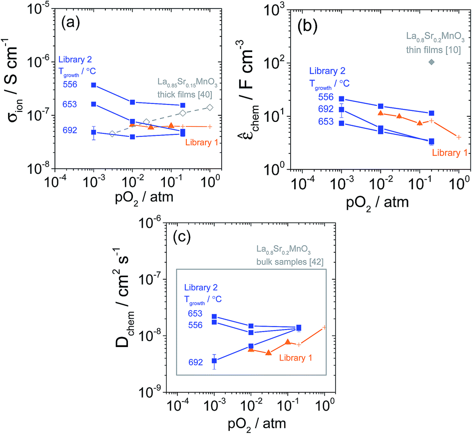 | ||
| Fig. 18 Through-film ionic conductivity σion (a), volume-normalized chemical capacitance chem (b), and ambipolar diffusivity Dchem (c) of (La0.8Sr0.2)0.95MnO3+δ obtained from 200 μm diameter microelectrodes at ∼710 °C. 95% confidence intervals are shown except where smaller than the markers. For Library 1, negligible thickness dependence was observed, and the data shown are an average over the eighteen measured film thicknesses. The data at 0.2 and 1 bar are shown with different markers because the values of Rion were fixed in the impedance fits at those conditions. For Library 2, the data at three growth temperatures are shown. Comparable literature data are shown in (a) for La0.85Sr0.15MnO3+δ thick films,40 (b) for La0.8Sr0.2MnO3+δ thin films,10 and in (c) for La0.8Sr0.2MnO3+δ bulk samples as a box that bounds the range of values measured.42 | ||
5. Summary and concluding remarks
Libraries containing hundreds of LSM thin film microelectrodes with systematically varied thickness or growth temperature were prepared and characterized. An automated impedance microprobe was developed to measure the electrochemical impedance response of such thin film microelectrodes in automated fashion. The electrochemical impedance response of the LSM microelectrodes at ∼710 °C was found to be well fit by a physically-derived equivalent circuit, and all trends were consistent with a pathway involving oxygen reduction over the entire surface of the LSM microelectrode followed by diffusion through the film and into the YSZ electrolyte. The surface activity was found to scale linearly with the area density of grain boundary length on the LSM microelectrode surface, suggesting that grain boundaries are more active than boundary-free surfaces towards the rate-limiting surface step. Film transport properties moreover support recent proposals that oxygen transport rates are enhanced in the grain boundaries relative to that in the bulk.The results underscore the importance of employing physically grounded models in analyzing impedance spectra. In the absence of such a model, the observation of increasing total electrode impedance with increasing LSM film thickness can easily be misinterpreted as arising from a diffusion-limited process. The findings further emphasize the importance of independently assessing film characteristics, in this case morphology, to uncover fundamental structure–property relations.
A question that naturally arises is whether and how the insights from this work can be applied to SOFC cathode design. Conventional LSM/YSZ composite cathodes have a 3PB![[thin space (1/6-em)]](https://www.rsc.org/images/entities/char_2009.gif) :2PB ratio that is roughly 100 times that of the model electrodes measured in the current study.43 Thus, the present results, collected in a configuration that inherently favors the 2PBs, do not exclude the possibility that the 3PBs dominate in a real device. Nevertheless, since the grain size in such cathodes, typically 3 to 5 μm, is not much greater than the critical thickness determined here, and since cathodic overpotentials (as would be found during operation) tend to increase the relative contribution of the bulk pathway,3 the electrocatalytic activity of the LSM/air interface may be relevant in conventional porous cathodes. In that case, the above results suggest it may be possible to improve the performance of commercially relevant electrodes by nanostructuring the LSM surface so as to increase the area density of exposed grain boundaries.
:2PB ratio that is roughly 100 times that of the model electrodes measured in the current study.43 Thus, the present results, collected in a configuration that inherently favors the 2PBs, do not exclude the possibility that the 3PBs dominate in a real device. Nevertheless, since the grain size in such cathodes, typically 3 to 5 μm, is not much greater than the critical thickness determined here, and since cathodic overpotentials (as would be found during operation) tend to increase the relative contribution of the bulk pathway,3 the electrocatalytic activity of the LSM/air interface may be relevant in conventional porous cathodes. In that case, the above results suggest it may be possible to improve the performance of commercially relevant electrodes by nanostructuring the LSM surface so as to increase the area density of exposed grain boundaries.
Acknowledgements
The authors would like to thank McAllister Technical Services for their help in designing and assembling the automated impedance microprobe, and Ben Meyers and Xinqi Chen at Northwestern University for their assistance in performing the FIB-SEM and SIMS characterization, respectively. This work was funded by the National Science Foundation via awards DMR-0520565 and EFRI-1038307, the Resnick Sustainability Institute at the California Institute of Technology, the National Central University of Taiwan, and the W. M. Keck Foundation. Selected facilities used were supported by the National Science Foundation via Northwestern University's MRSEC, DMR-1121262. (Opinions, findings, and conclusions or recommendations expressed in this material are those of the authors and do not necessarily reflect the views of these funding agencies.)References
- W. C. Chueh and S. M. Haile, Annu. Rev. Chem. Biomol. Eng., 2012, 3, 313–341 CrossRef CAS PubMed.
- Fuel Cell Handbook, U.S. Department of Energy, 2004 Search PubMed.
- S. Adler, Chem. Rev., 2004, 104, 4791–4843 CrossRef CAS PubMed.
- V. Brichzin, J. Fleig, H. U. Habermeier and J. Maier, Electrochem. Solid-State Lett., 2000, 3, 403–406 CrossRef CAS.
- V. Brichzin, J. Fleig, H. U. Habermeier, G. Cristiani and J. Maier, Solid State Ionics, 2002, 152, 499–507 CrossRef.
- J. Fleig, H. R. Kim, J. Jamnik and J. Maier, Fuel Cells, 2008, 8, 330–337 CrossRef CAS.
- T. Ioroi, T. Hara, Y. Uchimoto, Z. Ogumi and Z. Takehara, J. Electrochem. Soc., 1997, 144, 1362–1370 CrossRef CAS.
- E. Koep, D. S. Mebane, R. Das, C. Compson and M. L. Liu, Electrochem. Solid-State Lett., 2005, 8, A592–A595 CrossRef CAS.
- G. J. la O' and Y. Shao-Horn, Electrochem. Solid-State Lett., 2009, 12, B82–B85 CrossRef.
- G. J. la O', B. Yildiz, S. McEuen and Y. Shao-Horn, J. Electrochem. Soc., 2007, 154, B427–B438 CrossRef.
- A. M. Saranya, D. Pla, A. Morata, A. Cavallaro, J. Canales-Vazquez, J. A. Kilner, M. Burriel and A. Tarancon, Adv. Energy Mater., 2015, 5, 6 Search PubMed.
- A. Endo, M. Ihara, H. Komiyama and K. Yamada, Solid State Ionics, 1996, 86–88, 1191–1195 CrossRef CAS.
- L. Yan, K. R. Balasubramaniam, S. L. Wang, H. Du and P. A. Salvador, Solid State Ionics, 2011, 194, 9–16 CrossRef CAS.
- R. Radhakrishnan, A. V. Virkar and S. C. Singhal, J. Electrochem. Soc., 2005, 152, A210–A218 CrossRef CAS.
- T. M. Huber, M. Kubicek, A. K. Opitz and J. Fleig, J. Electrochem. Soc., 2015, 162, F229–F242 CrossRef CAS.
- G. Bergerhoff and I. D. Brown, Crystallographic Databases, International Union of Crystallography, Chester, 1987 Search PubMed.
- A. J. Zambano, H. Oguchi, I. Takeuchi, Y. Choi, J. S. Jiang, J. P. Liu, S. E. Lofland, D. Josell and L. A. Bendersky, Phys. Rev. B: Condens. Matter Mater. Phys., 2007, 75, 7 CrossRef.
- S. H. Lim, M. Murakami, J. H. Yang, S. Y. Young, J. Hattrick-Simpers, M. Wuttig, L. G. Salamanca-Riba and I. Takeuchi, Appl. Phys. Lett., 2008, 92, 3 Search PubMed.
- S. P. Jiang and J. G. Love, Solid State Ionics, 2001, 138, 183–190 CrossRef CAS.
- Z. H. Cai, M. Kubicek, J. Fleig and B. Yildiz, Chem. Mater., 2012, 24, 1116–1127 CrossRef CAS.
- D. Necas and P. Klapetek, Cent. Eur. J. Phys., 2012, 10, 181–188 Search PubMed.
- J. Januschewsky, M. Ahrens, A. Opitz, F. Kubel and J. Fleig, Adv. Funct. Mater., 2009, 19, 3151–3156 CrossRef CAS.
- P. Plonczak, A. Bieberle-Hutter, M. Sogaard, T. Ryll, J. Martynczuk, P. V. Hendriksen and L. J. Gauckler, Adv. Funct. Mater., 2011, 21, 2764–2775 CrossRef CAS.
- O. Durand, A. Letoublon, D. J. Rogers and F. H. Teherani, Thin Solid Films, 2011, 519, 6369–6373 CrossRef CAS.
- I. Petrov, P. B. Barna, L. Hultman and J. E. Greene, J. Vac. Sci. Technol., A, 2003, 21, S117–S128 Search PubMed.
- W. Lai and S. M. Haile, J. Am. Ceram. Soc., 2005, 88, 2979–2997 CrossRef CAS.
- J. Jamnik and J. Maier, J. Electrochem. Soc., 1999, 146, 4183–4188 CrossRef CAS.
- E. Barsoukov and J. Macdonald, Impedance Spectroscopy: Theory, Experiment, and Applications, Wiley-Interscience, New York, 2005 Search PubMed.
- J. Newman, J. Electrochem. Soc., 1966, 113, 501–502 CrossRef CAS.
- J. Park and R. Blumenthal, J. Electrochem. Soc., 1989, 136, 2867–2876 CrossRef CAS.
- K. A. Sasaki, Y. Hao and S. M. Haile, Phys. Chem. Chem. Phys., 2009, 11, 8349–8357 RSC.
- J. Maier, Physical Chemistry of Ionic Materials: Ions and Electrons in Solids, 2004 Search PubMed.
- J. Mizusaki, N. Mori, H. Takai, Y. Yonemura, H. Minamiue, H. Tagawa, M. Dokiya, H. Inaba, K. Naraya, T. Sasamoto and T. Hashimoto, Solid State Ionics, 2000, 129, 163–177 CrossRef CAS.
- I. Yasuda and M. Hishinuma, Solid State Ionics, 1995, 123, 382–390 CrossRef.
- H. Kamata, Y. Yonemura, J. Mizusaki, H. Tagawa, K. Naraya and T. Sasamoto, J. Phys. Chem. Solids, 1995, 56, 943–950 CrossRef CAS.
- F. W. Poulsen, Solid State Ionics, 2000, 129, 145–162 CrossRef CAS.
- A. Wedig, M. E. Lynch, R. Merkle, J. Maier and M. Liu, Ionic and Mixed Conducting Ceramics 8, 2012, vol. 45, pp. 213–224 Search PubMed.
- E. Navickas, T. M. Huber, Y. Chen, W. Hetaba, G. Holzlechner, G. Rupp, M. Stoger-Pollach, G. Friedbacher, H. Hutter, B. Yildiz and J. Fleig, Phys. Chem. Chem. Phys., 2015, 17, 7659–7669 RSC.
- R. A. de Souza, J. A. Kilner and J. F. Walker, Mater. Lett., 2000, 43, 43–52 CrossRef CAS.
- W. H. Huang, S. Gopalan and U. Pal, J. Power Sources, 2007, 173, 887–890 CrossRef CAS.
- C. K. Yang, Y. Yamazaki, A. Aydin and S. M. Haile, J. Mater. Chem. A, 2014, 2, 13612–13623 RSC.
- T. Bak, J. Nowotny, M. Rekas, C. C. Sorrell and E. R. Vance, Solid State Ionics, 2000, 135, 557–561 CrossRef CAS.
- J. R. Wilson, A. T. Duong, M. Gameiro, H.-Y. Chen, K. Thornton, D. R. Mumm and S. A. Barnett, Electrochem. Commun., 2009, 11, 1052–1056 CrossRef CAS.
Footnotes |
| † Electronic supplementary information (ESI) available. See DOI: 10.1039/c5ta02428e |
| ‡ Current address: Materials Science and Engineering, Northwestern University, Evanston, IL, USA; E-mail: sossina.haile@northwestern.edu |
| This journal is © The Royal Society of Chemistry 2015 |