
 Open Access Article
 This Open Access Article is licensed under a
 Creative Commons Attribution 3.0 Unported Licence
Aerosol assisted chemical vapour deposition of Ga-doped ZnO films for energy efficient glazing: effects of doping concentration on the film growth behaviour and opto-electronic properties†
Shuqun
Chen
a,
Giorgio
Carraro
b,
Davide
Barreca
c,
Andrei
Sapelkin
d,
Wenzhi
Chen
e,
Xuan
Huang
e,
Qijin
Cheng
e,
Fengyan
Zhang
e and
Russell
Binions
*a
aSchool of Engineering and Materials Science, Queen Mary University of London, London E1 4NS, UK. E-mail: r.binions@qmul.ac.uk
bDepartment of Chemistry and INSTM, Padova University, 35131 Padova, Italy
cCNR-IENI and INSTM, Department of Chemistry, Padova University, 35131 Padova, Italy
dDepartment of Physics and Astronomy, Queen Mary University of London, London E1 4NS, UK
eSchool of Energy Research, Xiamen University, Xiamen 361005, China
First published on 19th May 2015
Abstract
High quality Ga-doped ZnO thin films for use as energy efficient glazing coatings were deposited onto glass substrates by low cost single source aerosol assisted chemical vapour deposition (AACVD) of zinc and gallium acetylacetonates (in methanol) at a temperature of 350 °C. The effect of Ga content ranging from 0.4 at% to 6.1 at% on the structural and functional properties of ZnO films was investigated. Highly c-axis oriented films are easily formed in the case of pure ZnO with hexagonal (002) surfaces observed. This texture is gradually weakened in 0.4 at% to 3.0 at% Ga doped samples, and the deposit morphology is transformed to granular particles, irregular platelets, agglomerated particles and wedge-like structures, respectively, which may result from retarded grain boundary growth and increasing exposed non-(002) surfaces. Further gallium addition to 4.3 at% suppresses the grain growth and deteriorates the system crystallinity, with a concomitant change to a (102) preferential orientation in the heavily 6.1 at% Ga doped sample. The ZnO:Ga coatings exhibit high carrier concentration (up to 4.22 × 1020 cm−3) and limited carrier mobility (<5 cm2 V−1 s−1), and the minimum resistivity value obtained is 1.16 × 10⁻² Ω cm. Due to their large band gaps (3.14–3.42 eV) and favourable carrier numbers, high visible transmittance (83.4–85.3%) and infrared reflection (up to 48.9% at 2500 nm) are observed in these films, which is one of the best AACVD ZnO reported for low emissivity application and close to the optical requirements for commercial energy saving glazing.
1. Introduction
The energy required for the heating and cooling of modern buildings accounts for around 40% of global energy consumption and 30% of all carbon dioxide emissions.1,2 These numbers will continue to grow as increasingly larger areas of the world become developed and greater numbers of buildings are constructed.3 A variety of approaches, such as installing more efficient heating (e.g. heat pumps rather than electric hot water systems4), cooling (e.g. green roofs5) or renewable power systems (e.g. solar energy as a power source6), have been applied to reduce building energy demand. Moreover, the usage of energy saving glazing is another effective solution because untreated glass is a poor heat insulator whereby windows become a major heat transfer path between the inside and outside of buildings, resulting in unwanted heat loss or input.7 This is especially true in modern architecture, where a larger proportion of the exterior wall is designed and constructed with glass façades to be aesthetically pleasing and space efficient, but also provides an additional challenge to its thermal efficiency.3 Low emissivity (low-E) insulating windows are one kind of energy efficient glazing specifically designed for cold climate dominant areas. The use of spectrally selective coatings on the glass surface maintains transparency in solar wavelengths (0.3 to 2.5 μm) and reflective in the thermal radiation range (3.0 to 50 μm), which helps to minimize the heat transfer and therefore reduce heat loss.8,9 The European Commission aims at a 20% improvement in energy efficiency and 20% reduction in greenhouse gas emissions by 2020 (Horizon 2020),10 and suggests that up to 30% of the reduction targets for building sector could be achieved with low-E glazing.11Transparent conducting oxides (TCO) with a large enough band gap to transmit the visible spectrum of light and with a high charge carrier concentration to reflect infrared radiation can be used as low-E coatings.8,12 One typical example is Pilkington K-glass, where a thin fluorine-doped tin oxide (FTO) coating is deposited on a glass surface by an atmospheric pressure chemical vapour deposition (CVD) process.13 In recent years, wide-band-gap zinc oxide has been investigated as new energy efficient coating because it is cheap, biocompatible, chemically stable and easy to fabricate.14–16 The intrinsic ZnO, however, has a low electron concentration of 1018 to 1019 cm−3 (ref. 17) and doping becomes an indispensable approach to meet the low-E optical requirements. Among group-III elements (such as Al, Ga and In), common n-type dopants in ZnO, gallium is regarded as a better choice because its ionic and covalent radii (0.62, 1.26 Å) is closer to those of zinc (0.74, 1.31 Å) than to those of aluminium (0.5, 1.26 Å) or indium (0.81, 1.44 Å), so the lattice distortion under a high doping input can be minimized.18–20 In addition, Ga is relatively oxidation resistant, so the formation of non-conductive gallium oxide in ZnO can be suppressed.21,22
High quality ZnO:Ga films (carrier density superior to 1020 cm−3) can be produced by magnetron sputtering,18 pulsed laser deposition24 and spray pyrolysis25 on glass substrates, but they are hardly fabricated by conventional CVD processes probably due to the absence of appropriate Zn and/or Ga precursors. In recent years, aerosol assisted CVD (AACVD) has been increasingly utilized to fabricate TCO materials because it could provide a wider availability of precursors for high quality CVD products.26–28 The architecture of AACVD thin films can be easily tailored by tuning deposition conditions, i.e. the physical properties of the carrier solvent (boiling point, heat of combustion and viscosity), the gas flow rate and the substrate temperature.29–31 This is important because the morphology of a film could directly influence its optical performance and application.32 For instance, to improve the absorption efficiency of silicon thin film solar cells, a ZnO layer with rough pyramid-like surfaces can be introduced to scatter and trap light into the absorber material,33,34 whereas low-sized surface features make the coatings suitable for architectural glazing.14 Moreover, for TCO material deposition, the introduction of doping atoms could also alter film growth processes, resulting in different film structure and spatial organization. As a result, the morphology and bulk properties of TCO films can be modified by adding various type and amount of dopant material. A variety of dopant elements, including Al, Ga, In, F, Cu and Ag, in ZnO film deposition has been reported in earlier AACVD works.14,35–37 However, to our knowledge, there has been hardly any systematic study on the structural and functional properties of AACVD zinc oxide films as a function of doping concentration.
Based on the above observations, in this work, a detailed investigation of the influence of Ga content on the growth behaviour and functional properties of ZnO films prepared by AACVD process has been undertaken. The main goal of this work was to characterize the film composition, structure, morphology, electrical and optical properties as a function of doping content, discussing the interplay between the system structural parameters and opto-electronic performances.
2. Experimental section
2.1 Synthesis
AACVD was carried out in a horizontal bed cold-walled tubular reactor (dimensions 17 cm × 6 cm). The precursor solution was made by mixing 1.2 g zinc-acetylacetonate-monohydrate (Aldrich) and various amount of gallium-acetylacetonate (99.99%, Aldrich) ranging from 0.016 g to 0.16 g (Ga/Zn molar ratio from 0.5% to 5%) in 120 mL methanol (≫99.6%, Sigma-Aldrich). After placing the mixture in a glass bubbler, an aerosol mist was created using a piezoelectric device and then transported to the reaction chamber by 2 L min−1 flowing nitrogen gas (99.9%, BOC). Deposition was carried out on silica coated-barrier glass (50 nm SiO2 was coated on one side of float glass to prevent unwanted leaching of ions from the glass into the thin films38). The substrate temperature was kept at 350 °C and the deposition time was 90 min. For a successful deposition, a uniform area in the middle of the glass substrate can be observed (see Fig. S1†), and this area was subsequently selected for materials characterization.2.2 Characterization
Film surface elemental analysis was performed on a Perkin Elmer Φ 5600ci X-ray photoelectron spectroscopy (XPS) at a pressure lower than 10−8 mbar, using a non-monochromatized MgKα excitation source (1253.6 eV). The spectrometer was calibrated by assigning to the Au 4f7/2 line the Binding Energy (BE) of 84.0 eV with respect to the Fermi level and charging effects were corrected assigning to the C 1s line of adventitious carbon a value of 284.8 eV. Atomic composition (at%) was estimated using sensitivity factors provided by Φ V5.4A software. Sputtering treatments were carried out by Ar+ bombardment at 3.5 kV, with an argon partial pressure of ≈5 × 10⁻⁸ mbar. Samples were introduced directly by a fast entry lock system into the analytical chamber. Glancing incidence X-ray diffraction (GIXRD) measurements were made to identify phase constitutions on a PANalytical X'Pert Pro diffractometer in a glancing angle (α = 3°) mode using a CuKα X-ray source (Kα1 = 0.1540598 nm; Kα2 = 0.15444260 nm). The diffraction patterns were collected over 10–70° with a step size of 0.03° and a step time of 1.7 s per point. The surface morphology was evaluated using a FEI Inspect F Field Emission scanning electron microscope (SEM) at an accelerating voltage of 10 keV and spot size of 3.5 mm. Film thickness (shown in Table 1) was measured by cross-sectional images. High resolution transmission electron microscope (HRTEM) images and selected area electron diffraction (SEAD) patterns of ZnO:Ga films were collected using a FEI Tecnai F30 FEG operated at 300 kV. Root mean square roughness (RRMS) of the film surfaces were measured on a NT-MDT NTEGRA atomic force microscopy (AFM) over an area of 5 μm × 5 μm. Semicontact mode imaging was performed under air ambient conditions using silicon tips (Acta-20-Appnano ACT tapping mode with aluminium reflex coating, Nanoscience instruments) with a resonant frequency of 300 kHz and a spring constant of 40 N m−1. Electrical properties of films were studied by the van der Pauw method at room temperature using an Ecopia HMS-3000 hall measurement system. Square-cut samples (1 cm × 1 cm) were subjected to a 0.58 T permanent magnet and a current of 0.5 mA during the measurement. Photoluminescence (PL) spectroscopy was performed at room temperature using a micro-Raman system in co-ordination with a He:Cd CW laser Triax 320 (325 nm exciation, 1200/1 mm grating, 30 mW output power). UV/Vis/near IR transmission and reflection spectra were recorded in the range of 300 to 2500 nm using a Perkin-Elmer Fourier Transform Lambda 950 UV-Vis-NIR spectrometer. The transmission spectra background was taken against an air background. The average visible light transmittance (380 nm to 780 nm) of the studied glasses was computed according to the British Standard EN 673.| Sample I.D. | Elemental composition [at%] | Film thickness [μm] | TC (hkl) | Lattice constant a [Å] | Lattice constant c [Å] | Surface roughness [nm] | ||||||
|---|---|---|---|---|---|---|---|---|---|---|---|---|
| Zn | O | Ga | (002) | (101) | (102) | (103) | (112) | |||||
| ZnO | 46.9 | 53.1 | 0 | 0.76 | 3.51 | 0.03 | 0.30 | 1.05 | 0.12 | 3.2504 | 5.2082 | 13.5 |
| ZnO:Ga(0.4) | 42.2 | 57.8 | Not detected | 0.41 | 3.01 | 0.09 | 0.58 | 1.03 | 0.28 | 3.2501 | 5.2101 | 8.2 |
| ZnO:Ga(0.8) | 46.1 | 53.1 | 0.8 | 0.49 | 2.78 | 0.13 | 0.77 | 0.98 | 0.34 | 3.2518 | 5.2107 | 28.2 |
| ZnO:Ga(2.3) | 46.2 | 51.5 | 2.3 | 0.72 | 2.66 | 0.14 | 0.91 | 0.90 | 0.39 | 3.2511 | 5.2102 | 36.8 |
| ZnO:Ga(3.0) | 45.4 | 51.5 | 3.0 | 0.48 | 2.01 | 0.29 | 1.12 | 0.94 | 0.63 | 3.2504 | 5.2067 | 14.1 |
| ZnO:Ga(4.3) | 43.9 | 51.8 | 4.3 | 0.51 | 1.54 | 0.70 | 1.36 | 0.79 | 0.62 | 3.2527 | 5.2063 | 7.1 |
| ZnO:Ga(6.1) | 41.8 | 52.1 | 6.1 | 0.49 | 0.68 | 1.27 | 1.61 | 0.68 | 0.76 | 3.2530 | 5.1921 | 4.6 |
3. Results and discussion
3.1 Chemical composition of ZnO and ZnO:Ga films
Surface elemental analysis of ZnO and ZnO:Ga films with different Ga content was carried out by using XPS and the spectra are presented in Fig. 1. The survey spectra of studied samples indicate the presence of carbon, oxygen, zinc and gallium photoelectron and Auger signals. No other elements were detected in appreciable amounts. After a few minutes of Ar+ erosion, carbon signals were significantly reduced, indicating thus that contamination was mainly limited to the sample surface.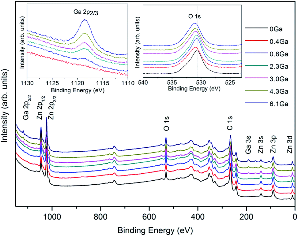 | ||
| Fig. 1 Wide-scan XP spectra of ZnO and ZnO:Ga films with various Ga contents. The insets show the Ga 2p3/2 and O 1s XP bands. | ||
Irrespective of the specific processing conditions, Zn 2p3/2 peak positions (average BE = 1021.3 eV) pointed out the presence of Zn(II) in ZnO environment. This indication could be confirmed by the analysis of the Zn LMM Auger signal and the calculation of the corresponding Auger parameters [αZn = BE(Zn 2p3/2) + KE(Zn LMM) = 2010.4 eV] further verify this indication.39,40 The insets of Fig. 1 display high-resolution Ga 2p3/2 and O 1s XPS photoelectron signals. The Ga 2p3/2 peak position and shape indicate the presence of Ga(III) in an oxide environment.41,42 In addition, the intensity of the Ga 2p3/2 signal is monotonically enhanced with an increase of gallium dopant content, indicating a progressive enhancement of Ga content in the obtained systems (compare Table 1). Regarding oxygen, the main peak is centred at 530.1 eV, in agreement with the position expected for O in ZnO lattice.43 The asymmetry of the O 1s signals on the high BE side at ≈531.8 eV suggests the co-presence of hydroxyl groups.39,40 Moreover, it is seen that an increase in the Ga content in the specimens produced a concomitant chemical shift to higher BEs of the main O 1s component. This phenomenon can be attributed to the fact that Ga atoms are bonded more strongly to oxygen, as the Ga–O covalent bond length is smaller than that of Zn–O.18,23 Due to the low gallium loading, the Ga 2p3/2 peak signal in the first doped sample was undetectable by XPS measurement and the Ga atomic content in other five ZnO:Ga films can be calculated at 0.8 at%, 2.3 at%, 3.0 at%, 4.3 at% and 6.1 at%, respectively. In spite of this, we can still estimate its content to be approximately 0.4 at% based on a linear relationship between the nominal Ga/Zn molar ratio in precursor solutions and the final gallium content in films, as illustrated in Fig. S2.† The details of the film elemental composition and the corresponding sample I.D. are listed in Table 1.
3.2 Structural properties of ZnO and ZnO:Ga films
Crystal structures of ZnO and ZnO:Ga films with various doping contents were analysed by GIXRD. As shown in Fig. 2, all the reflection signals can be matched to the standard diffraction pattern of hexagonal wurzite phase ZnO (JCPDS 36-1451).44 Moreover, the pure ZnO exhibits a very strong c-axis texture, as often reported,43,45 and the introduction of gallium dopants weakens this texture to some degree. This indicates the growth of (002)-oriented crystals is less favoured in doped samples. The (002) peak still dominates in the patterns of ZnO with Ga content lower than 2.3 at%. Further addition of gallium atoms to 3.0 at% results in a reduction of peak intensity associated with emergence of new peaks, such as (100) and (110). The film crystallinity of heavily doped ZnO:Ga(4.3) and ZnO:Ga(6.1) sample is quite poor and the crystallites are more randomly oriented. In order to attain a deeper insight into the texturing phenomenon, a texture coefficient, TC (hkl), is introduced to estimate the degree of film orientation46 and the calculated results for present films are summarized in Table 1. As observed, pure ZnO exhibits a high (002) texture coefficient of 3.51, representing a significant c-axis preferred orientation, and this value decreases continuously from 3.01 in ZnO:Ga(0.4) to 2.01 in ZnO:Ga(3.0), which is mainly compensated by an enhanced texture coefficient in (102) plane. Further increase of Ga atoms would suppress the (002) plane growth greatly and the preferred orientation is changed to (102) in ZnO:Ga(6.1).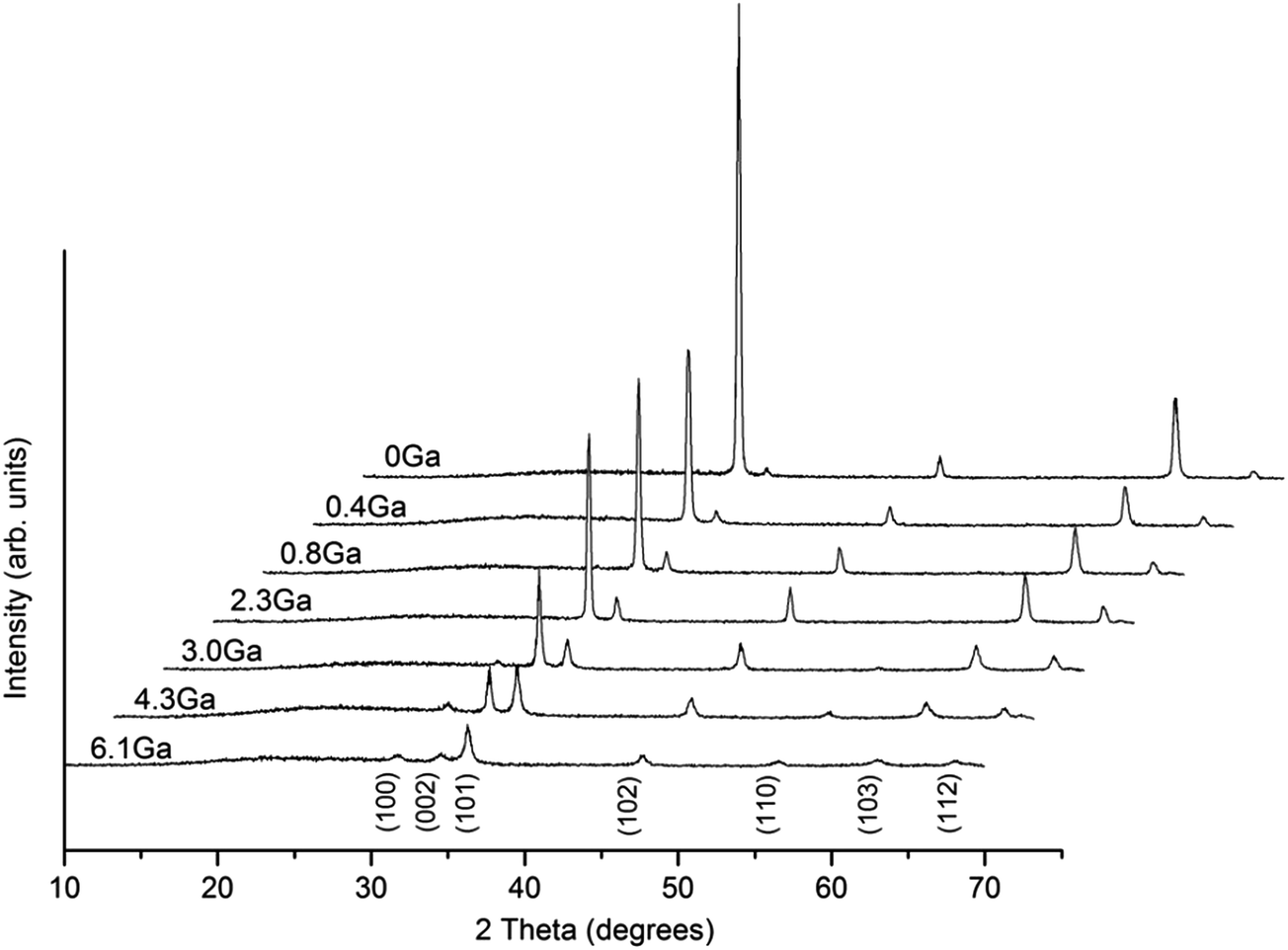 | ||
| Fig. 2 GIXRD patterns of ZnO and ZnO:Ga films with various Ga contents. | ||
The lattice parameters, a and c, of hexagonal ZnO and ZnO:Ga films are listed in Table 1. Among five strong c-axis oriented samples, the c value in pure ZnO is lower than that of others except for the ZnO:Ga(3.0). This result might be apparently surprising because Ga3+ holds a smaller ionic radius with respect to Zn2+, whereby the substitution of Zn2+ with Ga3+ at lattice sites could decrease the lattice constant.23 The first possible reason could due to the presence of high oxygen vacancy density in ZnO causing lattice distortion and decreasing the interplanar spacing.47,48 The existence of oxygen vacancies is indeed demonstrated by the analysis of film electrical properties, where the ZnO obtains a carrier density of 0.2 × 1020 cm−3. Fig. 3 shows the photoluminescence spectra of pure ZnO and two doped samples ZnO:Ga(0.4) and ZnO:Ga(3.0). The spectra display two intense peaks near 540 nm and 610 nm. It is generally believed the green emission at 540 nm is due to transition in defects, in particular the oxygen vacancies.49–51 The orange emission at 610 nm is less commonly reported, and could be related to the presence of interstitial oxygen ions.52,53 The reduced peak intensity at 540 nm indicates the generation of oxygen vacancies in ZnO is suppressed with Ga addition since the oxygen atoms are boned more strongly.54,55 The other more likely reason is the existence of interstitial gallium atoms in ZnO lattice, which expands the lattice parameters considerably.56 Also this kind of defect is hard to avoid under non-vacuum deposition conditions. Therefore, larger c-axis lattice constants are observed in ZnO:Ga(0.4) to ZnO:Ga(2.3) compared with pure ZnO. A further increase of Ga content to 3.0 at% starts suppressing the c-axis oriented crystal growth, associated with a reduction of (002) peak intensity, and the lattice parameter decreases to a value of 5.2067 Å. For ZnO:Ga(4.3) and ZnO:Ga(6.1), the crystal lattice is heavily distorted and the (002) signal intensity is significantly lowered, leading to a minimum c value of 5.1921 Å. Also the general larger lattice parameter a in doped samples could due to the reduction of oxygen vacancies, existence of interstitial gallium atoms and the promotion of near a-axis oriented crystal growth. For example, the normal direction of (102) plane is 58.03° deviated from the c-axis,25 so the promoted (102) crystal growth could help increase the a parameter.
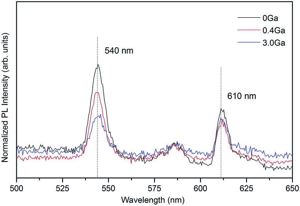 | ||
| Fig. 3 Room-temperature PL spectra of ZnO, ZnO:Ga(0.4) and ZnO:Ga(3.0) films. | ||
The interplay between Ga doping and morphology is shown by the SEM images in Fig. 4. It is seen that the pure ZnO is composed of uniform regular grains, with hexagonal faces parallel to the substrate, although not so obvious as those in ZnO nanorods.57 After adding 0.4 at% Ga, the hexagonal grains disappear and turn into granular particles, and then transform into irregularly shaped platelets in ZnO:Ga(0.8). Agglomerated particles exhibit in the sample with 2.3 at% Ga and the ZnO:Ga(3.0) film morphology is largely wedge-like in shape. Further Ga addition appears to suppress the grain growth and poorly connected particles are observed both in ZnO:Ga(4.3) and ZnO:Ga(6.1), a phenomenon which correlates with the reduced peak intensities in their XRD patterns. It is also worth mentioning that both pure ZnO and samples with a low doping level exhibit typical columnar grain structure, as seen from their cross-section SEM images in Fig. S3,† while the ZnO:Ga(4.3) and ZnO:Ga(6.1) are more likely thickened by overlapped particles without any evidence of macro-texture, indicating that coalescence processes are largely suppressed.
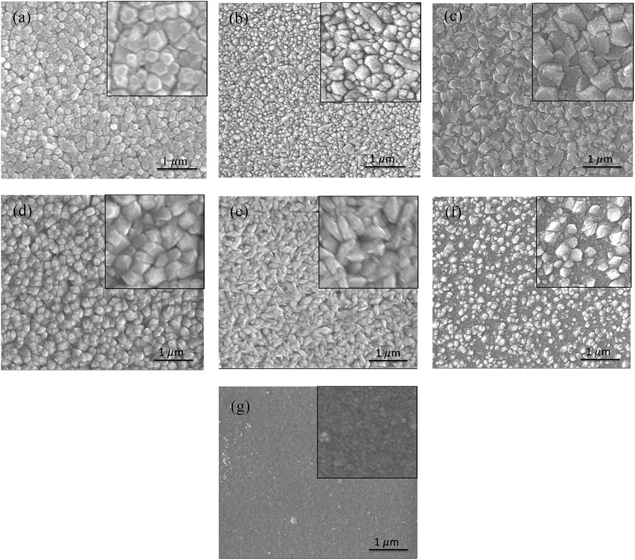 | ||
| Fig. 4 Plane-view SEM micrographs of (a) ZnO, (b) ZnO:Ga(0.4), (c) ZnO:Ga(0.8), (d) ZnO:Ga(2.3), (e) ZnO:Ga(3.0), (f) ZnO:Ga(4.3) and (g) ZnO:Ga(6.1) films. The insets show higher magnification images for each sample. | ||
The film crystallization occurs through sequential nucleation, initial growth and coalescence processes.58 Texture can be formed during the first nucleation stage, driven by surface energy minimization, or developed in the subsequent growth phase because only grains with lower surface energy can survive during the coalescence process.59 In pure ZnO, the polar (002) planes have higher surface energy, so the fastest crystal growth rate is usually along the c-axis to reduce the (002) facet areas as well as the system energy.60 Moreover, only those [002]-oriented crystallites with their c-axis orientation normal or near normal to the underlying substrate could grow all the way upwards, all differently oriented crystals stop their growth at earlier stages, resulting in columnar grain features and strong (002) texturing.61 The surface morphology of crystalline films is also affected by the preferred growth direction but in many cases they are more related to the exposed crystal planes. For instance, c-axis oriented ZnO films could preserve a hexagonal surface feature with their (002) planes exposed or exhibit a pyramidal structure by exposing the (101) planes, whose normal direction is 62° deviated from that of the basal (002) planes.62 The introduction of extrinsic doping atoms could greatly influence the ZnO film growth as well as the resulting morphology. On the one hand, the dopant atoms could alter the surface energy of crystallographic planes. For example, Liu et al. reported the growth of the a-axis-oriented (100) plane is more active than the growth of the c-axis-oriented (002) planes in ZnO:F films due to F− anions filling O vacancies or substituting O sites.63 This phenomenon would promote the growth of wedge-like grains parallel to the substrate rather than columnar ones.17 On the other hand, the dopant impurities are prone to segregating at the non-crystalline grain boundary areas, especially when the doping content suppresses its saturation point in ZnO, and drag the grain boundary movement, which reduce the grain size as well as the film crystallinity.64,65
For our pure ZnO sample, its pronounced columnar grains and strong (002) texture represent the microstructure evolution process have been fully developed. Also the observed hexagonal surface feature suggests the growth rate of ingrain and grain boundary areas are identical along the film thickening direction. For the coatings with a low doping level (0.4 at% to 3.0 at%), their highly c-axis oriented textures indicate (i) the (002) planes still hold much higher surface energy and growth rate than the others under the given gallium content, and (ii) the film coalescence processes are also greatly developed in these samples. In spite of this, the enhanced (102) texture coefficient suggests the incorporation of Ga atoms in ZnO lattice may increase the surface energy of (102) facets and populate their growth. A similar phenomenon has also been reported in Ga-doped ZnO nanowires, where the wire growth direction was changed from [001] direction in pure ZnO to [102] in ZnO:Ga samples.66 Thus, the c-axis textures are less significant in doped coatings and also weaken with increasing gallium content. Moreover, the grain boundary growth in ZnO:Ga samples would be retarded compared with the ingrain areas, resulting in the disappearance of hexagonal grains and the exposure of other low-index facets. These non-[002] oriented surfaces, which are formed at the final deposition stage, could successfully avoid to be incorporated into the columnar grain structure. It is likely that Ga will preferentially move to the polar (002) surfaces as a way of charge compensation in the crystal. This will also contribute to the retardation of growth in this direction. But in order to identify exactly which facets are exposed in ZnO:Ga(0.4) to ZnO:Ga(3.0), cross-section TEM investigation is required in our future work. When the Ga content exceeds 4.3 at%, the segregation of gallium atoms at grain boundaries become pronounced and suppress the grain growth greatly. So the [002]-oriented crystallites can no longer overgrow other crystallites with different orientations during the film thickening, leading to an obvious reduction in (002) peak intensity as well as the disappearance of a columnar texture structure. Also the obtained [102] preferential orientation in ZnO::Ga(6.1) should originate from a preferred nucleation in the early growth stage as the heavy doping inhibits all the crystallites growth significantly and refined grains are observed in this sample. The coarse grain boundaries, with amorphous-like contrast to the grain interiors, in its HRTEM image (Fig. 5) could verify the segregation of dopant atoms in ZnO:Ga(6.1). The doping dependent ZnO film growth behavior is schematically illustrated in Fig. S4.†
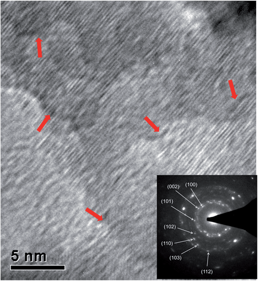 | ||
| Fig. 5 Bright field HRTEM images of the nanograins in ZnO:Ga(6.1). The inset shows the selected area electron diffraction pattern and the red arrows refer to grain boundary areas. | ||
3.3 Electrical properties of ZnO and ZnO:Ga films
The electrical parameters, including resistivity, Hall mobility and carrier concentration, of ZnO and ZnO:Ga films with doping content ranging from 0.4 at% to 6.1 at% were determined by Hall effect measurements via the van der Pauw method. The results in Table 2 show that all the films were n-type semiconductors and that Ga introduction has a limited influence on the film resistivity, while a large variation in the carrier density and mobility exists between the undoped and doped ZnO samples.| Sample I.D. | Carrier concentration | Carrier mobility | Resistivity | Resistance | Doping efficiency | T λ550 | T λ380−780 | Plasma wavelength | R λ2500 | Band gap |
|---|---|---|---|---|---|---|---|---|---|---|
| [×1020 cm−3] | [cm2 (V s)−1] | [×10−2 Ω cm] | [Ω sq−1] | [%] | [%] | [%] | [nm] | [%] | [eV] | |
| ZnO | 0.20 | 25.0 | 1.28 | 168.9 | — | 82.5 | 84.6 | — | — | 3.14 |
| ZnO:Ga(0.4) | 0.80 | 4.8 | 1.62 | 395.6 | 63.9 | 83.9 | 85.3 | — | — | 3.19 |
| ZnO:Ga(0.8) | 1.70 | 2.6 | 1.42 | 289.4 | 68.2 | 81.6 | 83.4 | 2440 | 17.5 | 3.27 |
| ZnO:Ga(2.3) | 3.55 | 0.9 | 1.92 | 266.8 | 45.0 | 83.4 | 83.6 | 1825 | 41.1 | 3.39 |
| ZnO:Ga(3.0) | 4.22 | 1.3 | 1.16 | 241.9 | 42.4 | 86.3 | 84.7 | 1670 | 48.9 | 3.40 |
| ZnO:Ga(4.3) | 3.60 | 0.6 | 2.97 | 582.4 | 25.6 | 86.5 | 84.5 | 1920 | 35.0 | 3.42 |
| ZnO:Ga(6.1) | 1.14 | 0.1 | 57.57 | 11![[thin space (1/6-em)]](https://www.rsc.org/images/entities/char_2009.gif) 749 749 |
5.8 | 83.6 | 84.7 | 2380 | 18.6 | 3.37 |
The pure ZnO film has a carrier concentration of 0.2 × 1020 cm−3 and these charge carriers can be identified as oxygen vacancies since the films are deposited under an oxygen-deficient atmosphere. The addition of Ga atoms enhances ZnO carrier density to a range of 1020 cm−3. As the Ga content increased, the concentration of carrier shows a rapid enhancement from 0.80 × 1020 cm−3 in ZnO:Ga(0.4) to 4.22 × 1020 cm−3 in ZnO:Ga(3.0), and then gradually decreases to 1.14 × 1020 cm−3 at higher Ga loadings. These concentration values are quite high and comparable to the previously reported values in sputtered ZnO:Ga films (upto ∼5 × 1020 cm−3).23,67 The electron carriers in gallium-doped ZnO films are generated by substituting Zn2+ ions with Ga3+ ions, and this substitution efficiency is essential for the film electrical performance because those inactive doping atoms, such as interstitial gallium atoms, cannot generate free electrons but act as electron scattering centres.17 The doping efficiency (ηDE) can be defined as the ratio of the electron concentration to the Ga atomic concentration in ZnO:Ga films under an assumption that every incorporated Ga cation provides one free electron with substitution of a Zn ion:17,68
 | (1) |
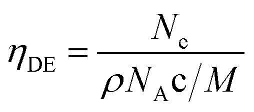
A high carrier mobility of 25.0 cm2 (V s)−1 can be observed in pure ZnO as such it is easy to appreciate that scattering by the carriers is limited. After the Ga atoms are introduced, the mobility values decrease dramatically. Upon enhancing Ga content, the mobility in ZnO:Ga samples declines gradually from a maximum value of 4.8 cm2 (V s)−1 in ZnO:Ga(0.4) to a lowest value of 0.1 cm2 (V s)−1 in ZnO:Ga(6.1). It is known that the mobility of free carrier is determined by the electron scattering arising mainly from grain boundaries, ionized impurities and neutral impurities in doped ZnO films.25 The dominance of the scattering effects varies with the carrier density and the potential barrier at the grain boundary has been considered to be negligible when the carrier concentration is superior to 1020 cm−3.69 Moreover, the ionized impurity scattering cannot be the only dominant mechanism in our case because even more charge carriers are generated by ionized impurities in sputtered ZnO:Ga films, their mobility (10–30 cm2 V−1 s−1) could still one order higher than our results.23,67 Thus, the inferior mobility performance in present samples could mainly result from an insufficient doping efficiency, where many inactive dopant atoms locate in the ZnO lattice as interstitial defects or segregate at grain boundary areas as neutral impurities. By comparison, the higher mobility values in sputtered ZnO:Ga coatings should due to an improved incorporation efficiency. We attribute this to the high vacuum condition during their depositions, which typically leads to films of higher purity and a reduced number of defects.70 In Fig. 6, the charge carrier mobility is plotted versus the carrier density and doping efficiency for the studied coatings. It is seen that the mobility values depend linearly on the doping efficiency, and a similar trend is also observed with respect to carrier density, except for the most heavily doped sample ZnO:Ga(6.1). This indicates the dominant electron scattering mechanism is transformed from a combined ionized and neutral impurity scattering in ZnO:Ga(0.4) to ZnO:Ga(4.3) to the neutral impurity scattering only in ZnO:Ga(6.1).
 | ||
| Fig. 6 The carrier mobility as a function of (a) carrier concentration and (b) doping efficiency for ZnO:Ga films. The dash circle marks the sample deviating from the linear trend. | ||
Through a combination of carrier concentration and mobility, a lowest resistivity value of 1.16 × 10⁻² Ω cm was obtained in ZnO:Ga(3.0) film with an estimated carrier density 4.22 × 1020 cm−3 and mobility 1.27 cm2 (V s)−1. Due to the inferior mobility performance, our film resistivity is one order of magnitude higher than previously reported highly conductive ZnO:Ga film.23,67 In spite of this, these coatings could still have a potential application in energy efficient glazing. According to our observations, carrier density is the most important electric parameter rather than resistivity, though clearly they are related.
3.4 Optical properties of ZnO and ZnO:Ga films
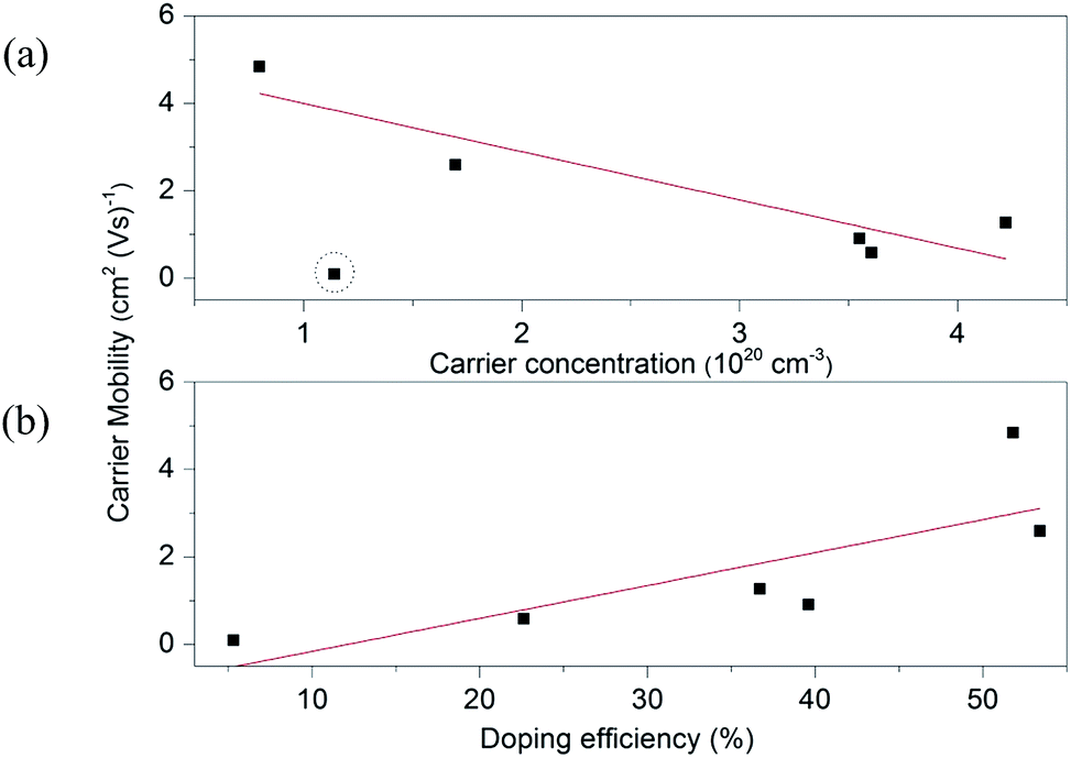
Fig. 7 shows the optical transmittance of pure ZnO and various ZnO:Ga films from 300 nm to 2500 nm and the reflectance of selected ZnO:Ga samples from 1000 nm to 2500 nm. It is seen that the ZnO:Ga coatings exhibit high transparency across the visible lights (>80% transmission across the visible portion of the spectrum, including the substrate absorbance, see Table 2) and good reflectivity in the near-infrared range (up to 48.9% reflection at 2500 nm). The films also display prominent interference fringes, which are caused by the multiple reflections at the three interfaces of the air/film/substrate bilayer,14 and the transmission of doped samples reduces rapidly in the near infrared region, compensated by a continuous reflection enhancement after a certain wavelength. | ||
| Fig. 7 (a) Optical transmission spectra of ZnO and various ZnO:Ga films. (b) Optical reflection spectra of selected ZnO:Ga films. | ||
The calculated average transmittance in the visible light region (380 nm to 760 nm) of pure ZnO and ZnO:Ga films are 84.6%, 85.3%, 83.4%, 83.6%, 84.7%, 84.5% and 84.7%, respectively, a little lower than the values in sputtered ZnO:Ga samples (90–95%),23,67 thus a majority of visible light could transmit through the coatings. The minor light loss in TCO films is expected to mainly depend on the light scattering as a function of grain size, surface roughness and the level of defects.71,72 Among the studied coatings, a high visible transmission value of 84.7% can be observed in ZnO:Ga(6.1) even though a greater number of boundary areas is existed in this sample because its grain size is much smaller than that of others. This indicates the grain boundary light scattering is unlikely to be the main reason for visible light loss. Furthermore, the transmittance of pure ZnO and ZnO:Ga(3.0) are basically same despite their large difference in carrier density, representing the carrier scattering effect is also limited for present samples. Based on this, the obtained lower transmission values in ZnO:Ga(0.8) and ZnO:Ga(2.3) could be due to their rougher surface. This idea can be directly verified by two representative AFM images in Fig. 8, where the most transparent sample ZnO:Ga(0.4) exhibits a low surface roughness of 8.2 nm and this value in ZnO:Ga(2.3) could reach as high as 36.8 nm.
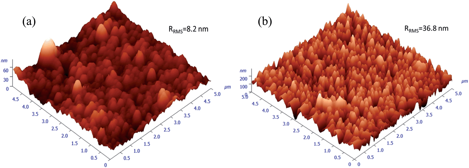 | ||
| Fig. 8 AFM images for samples (a) ZnO:Ga(0.4) and (b) ZnO:Ga(2.3). Roughness values of other samples are summarised in Table 1. | ||
The reduction of transmittance and increase of reflectivity in near infrared region in ZnO:Ga films are caused by a coherent oscillation of conduction electrons (plasmons) with incident electromagnetic radiation.73 The reflection onset occurs at the plasma wavelength (λp) which can be defined as follows:74
| λp2 = c2m*ε/Nee2 | (2) |
The optical band gaps of pure ZnO and various ZnO:Ga films were determined by constructing Tauc plots using the (ahv)2 relation.77 The resulting plots are shown in Fig. 9(a) and the corresponding values are listed in Table 2. It is seen the band gap of pure ZnO film at 3.14 eV is lower than the reported value of bulk ZnO (3.24 eV) and the introduction of Ga atoms could enhance this band gap obviously with a maximum value of 3.42 eV obtained in sample ZnO:Ga(4.3). Such a band-gap widening phenomenon has been reported in many literatures for doped ZnO and can be explained through the Burstein–Moss effect. Accordingly, the excess free electrons with the addition of donor Ga3+ ions would fill the bottom levels of conduction band, thereby leading to an increase in the Fermi level.58,78,79 This band gap broadening (ΔEg) is related to the electron concentration Ne through the following equation:80
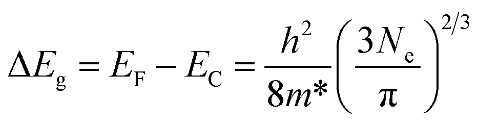 | (3) |
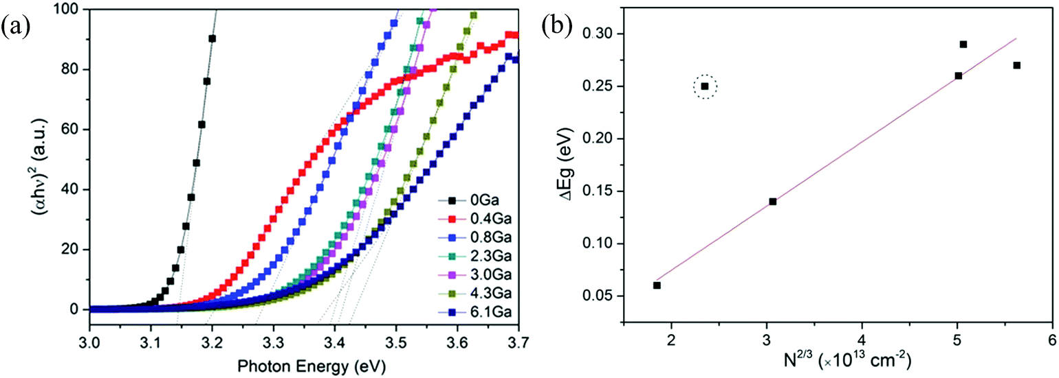 | ||
| Fig. 9 (a) Tauc plots of ZnO and ZnO:Ga films with various Ga contents. (b) The relationship between film carrier concentration and the band gap shift. The dash circle marks the sample deviating from the linear trend. | ||
4. Conclusions
Transparent conductive Ga-doped ZnO thin films were successfully deposited on glass substrate by AACVD process and the effect of Ga doping content on the growth behaviour and the functional properties of ZnO films were analysed. Highly c-axis oriented films are easily formed in the case of pure ZnO with hexagonal surface features. This texture is gradually weakened in 0.4 at% to 3.0 at% doped samples, and the film morphology is transformed to granular particles, irregularly platelets, agglomerated particles and wedge-like structure, respectively, resulting from retarded grain boundary growth and increasing exposed non-(002) surfaces. Further Ga addition to 4.3 at% suppress the grain growth and deteriorate the film crystallinity, and the preferential growth orientation is changed to (102) in heavily doped ZnO:Ga(6.1) film. High carrier density (up to 4.22 × 1020 cm−3) but inferior carrier mobility (<5 cm2 V−1 s−1) are observed in ZnO:Ga films, resulting in a minimum resistivity of 1.16 × 10⁻² Ω cm. The poor mobility performance is mainly originated from an insufficient doping efficiency with a high amount of inactive doping atoms cannot generate free electrons but act as electron scattering centres. In spite of this, high visible transmittance (averages between 83.4 and 85.3% across the visible portion of the spectrum) and good infrared reflection (up to 48.9% at 2500 nm) are still exhibited in the ZnO:Ga coatings due to their wide band gaps and favourable carrier densities. The optical performance of ZnO:Ga(3.0) film is close to the optical requirement for commercial low-E coating. We hope this study could provide valuable information on the fabrication and optimization of ZnO based energy efficient coating with a cost-effective approach.Acknowledgements
S.Q. Chen would like to thank the China Scholarship Council/Queen Mary University of London Joint PhD scholarship program. Dr Rory Wilson, Ms Fengfeng Zhang and Mr Congwei Wang are acknowledged for their appreciated assistance in this work. Pilkington-NSG is specially thanked for providing glass substrates. G.C. and D.B. kindly acknowledge the financial support from Padova University PRAT 2010 project (no. CPDA102579) and grant no. CPDR132937/13 (SOLLEONE).References
- I. P. Parkin and T. D. Manning, J. Chem. Educ., 2006, 83, 393 CrossRef CAS.
- M. E. A. Warwick and R. Binions, J. Mater. Chem. A, 2014, 2, 3275 CAS.
- M. E. A. Warwick, G. Hyett, I. Ridley, F. R. Laffir, C. Olivero, P. Chapon and R. Binions, Sol. Energy Mater. Sol. Cells, 2013, 118, 149–156 CrossRef CAS PubMed.
- R. Dowling, P. McGuirk and H. Bulkeley, Cities, 2014, 38, 18–24 CrossRef PubMed.
- I. Jaffal, S.-E. Ouldboukhitine and R. Belarbi, Renewable Energy, 2012, 43, 157–164 CrossRef PubMed.
- X. Guan, Z. Xu and Q.-S. Jia, IEEE Trans. Smart Grid, 2010, 1, 243–252 Search PubMed.
- Chemical Vapour Deposition, ed. A. C. Jones and M. L. Hitchman, Royal Society of Chemistry, Cambridge, 2008 Search PubMed.
- C. G. Granqvist, Sol. Energy Mater. Sol. Cells, 2007, 91, 1529–1598 CrossRef CAS PubMed.
- S.-Y. Li, G. A. Niklasson and C. G. Granqvist, Appl. Phys. Lett., 2011, 99, 131907 CrossRef PubMed.
- http://ec.europa.eu/clima/policies/package/ .
- http://www.glassforeurope.com/images/cont/117_57609_file.pdf.11 .
- S.-Y. Li, G. A. Niklasson and C. G. Granqvist, Appl. Phys. Lett., 2011, 99, 131907 CrossRef PubMed.
- D. S. Bhachu, M. R. Waugh, K. Zeissler, W. R. Branford and I. P. Parkin, Chem.–Eur. J., 2011, 17, 11613–11621 CrossRef CAS PubMed.
- D. S. Bhachu, G. Sankar and I. P. Parkin, Chem. Mater., 2012, 24, 4704–4710 CrossRef CAS.
- M. Rydzek, M. Reidinger, M. Arduini-Schuster and J. Manara, Thin Solid Films, 2012, 520, 4114–4118 CrossRef CAS PubMed.
- X. Chu, H. Tao, Y. Liu, J. Ni, J. Bao and X. Zhao, J. Non-Cryst. Solids, 2014, 383, 121–125 CrossRef CAS PubMed.
- Y.-J. Choi and H.-H. Park, J. Mater. Chem. C, 2014, 2, 98 RSC.
- X. Yu, J. Ma, F. Ji, Y. Wang, X. Zhang, C. Cheng and H. Ma, J. Cryst. Growth, 2005, 274, 474–479 CrossRef CAS PubMed.
- A. Z. Barasheed, S. R. S. Kumar and H. N. Alshareef, J. Mater. Chem. C, 2013, 1, 4122 RSC.
- S. Chen, M. E. A. Warwick and R. Binions, Sol. Energy Mater. Sol. Cells, 2015, 137, 202–209 CrossRef CAS PubMed.
- J. H. Kim, B. Du Ahn, C. H. Lee, K. A. Jeon, H. S. Kang and S. Y. Lee, J. Appl. Phys., 2006, 100, 113515 CrossRef PubMed.
- H. J. Ko, Y. F. Chen, S. K. Hong, H. Wenisch, T. Yao and D. C. Look, Appl. Phys. Lett., 2000, 77, 3761 CrossRef CAS PubMed.
- S. Liang and X. Bi, J. Appl. Phys., 2008, 104, 113533 CrossRef PubMed.
- S.-M. Park, T. Ikegami and K. Ebihara, Thin Solid Films, 2006, 513, 90–94 CrossRef CAS PubMed.
- A. Tiburcio-Silver, A. Sanchez-Juarez and A. Avila-Garcia, Sol. Energy Mater. Sol. Cells, 1998, 55, 3–10 CrossRef CAS.
- R. Elleuch, R. Salhi, N. Maalej, J.-L. Deschanvres and R. Maalej, Mater. Sci. Eng., B, 2013, 178, 1124–1129 CrossRef CAS PubMed.
- S. Chen, R. M. Wilson and R. Binions, J. Mater. Chem. A, 2015, 3, 5794–5797 CAS.
- P. Marchand, I. A. Hassan, I. P. Parkin and C. J. Carmalt, Dalton Trans., 2013, 42, 9406–9422 RSC.
- M. R. Waugh, G. Hyett and I. P. Parkin, Chem. Vap. Deposition, 2008, 14, 366–372 CrossRef CAS PubMed.
- M. A. Ehsan, H. N. Ming, M. Misran, Z. Arifin, E. R. T. Tiekink, A. P. Safwan, M. Ebadi, W. J. Basirun and M. Mazhar, Chem. Vap. Deposition, 2012, 18, 191–200 CrossRef CAS PubMed.
- K. Choy, Prog. Mater. Sci., 2003, 48, 57–170 CrossRef CAS.
- L. Chen, T.-M. Lu and G.-C. Wang, J. Appl. Phys., 2012, 112, 024303 CrossRef PubMed.
- J. Müller, B. Rech, J. Springer and M. Vanecek, Sol. Energy, 2004, 77, 917–930 CrossRef PubMed.
- C. Battaglia, J. Escarre, K. Söderström, F.-J. Haug, D. Dominé, A. Feltrin and C. Ballif, Mater. Res. Soc. Symp. Proc., 2011, 1245, A03–A04 Search PubMed.
- M. G. Nolan, J. A. Hamilton, S. O'Brien, G. Bruno, L. Pereira, E. Fortunato, R. Martins, I. M. Povey and M. E. Pemble, J. Photochem. Photobiol., A, 2011, 219, 10–15 CrossRef CAS PubMed.
- G. Walters and I. P. Parkin, Appl. Surf. Sci., 2009, 255, 6555–6560 CrossRef CAS PubMed.
- S. Chen, N. Noor, I. P. Parkin and R. Binions, J. Mater. Chem. A, 2014, 2, 17174–17182 CAS.
- N. Noor and I. P. Parkin, J. Mater. Chem. C, 2013, 1, 984 RSC.
- http://srdata.nist.gov/xps/ .
- C. D. Wagner, Handbook of x-ray photoelectron spectroscopy: a reference book of standard data for use in x-ray photoelectron spectroscopy, Physical Electronics Division, Perkin-Elmer Corp., 1979 Search PubMed.
- J. Zhang, X. F. Li, J. G. Lu, Z. Z. Ye, L. Gong, P. Wu, J. Huang, Y. Z. Zhang, L. X. Chen and B. H. Zhao, J. Appl. Phys., 2011, 110, 084509 CrossRef PubMed.
- M. Hellwig, K. Xu, D. Barreca, A. Gasparotto, M. Winter, E. Tondello, R. A. Fischer and A. Devi, Eur. J. Inorg. Chem., 2009, 2009, 1110–1117 CrossRef PubMed.
- D. Bekermann, A. Gasparotto, D. Barreca, L. Bovo, A. Devi, R. A. Fischer, O. I. Lebedev, C. Maccato, E. Tondello and G. Van Tendeloo, Cryst. Growth Des., 2010, 10, 2011–2018 CAS.
- Joint Committee Powder Diffraction Standards, Powder Diffraction File (Data File 36-1451).
- C. S. McNally, D. P. Turner, A. N. Kulak, F. C. Meldrum and G. Hyett, Chem. Commun., 2012, 48, 1490–1492 RSC.
- A. A. Ramadan, A. A. Abd El-Mongy, A. M. El-Shabiny, A. T. Mater, S. H. Mostafa, E. A. El-Sheheedy and H. M. Hashem, Cryst. Res. Technol., 2009, 44, 111–116 CrossRef CAS PubMed.
- E.-K. Jeong, D.-H. Kim, I.-S. Kim, and S.-Y. Choi, in ECS Transactions, ECS, 2007, vol. 11, pp. 193–201 Search PubMed.
- X.-L. Li, Z.-L. Wang, X.-F. Qin, H.-S. Wu, X.-H. Xu and G. A. Gehring, J. Appl. Phys., 2008, 103, 023911 CrossRef PubMed.
- Q. Cheng and K. Ken Ostrikov, CrystEngComm, 2011, 13, 3455 RSC.
- Q. Cheng and K. K. Ostrikov, ChemPhysChem, 2012, 13, 1535–1541 CrossRef CAS PubMed.
- C.-L. Hsu, S.-J. Chang, Y.-R. Lin, S.-Y. Tsai and I.-C. Chen, Chem. Commun., 2005, 3571–3573 RSC.
- S. O'Brien, L. H. K. Koh and G. M. Crean, Thin Solid Films, 2008, 516, 1391–1395 CrossRef PubMed.
- X. L. Wu, G. G. Siu, C. L. Fu and H. C. Ong, Appl. Phys. Lett., 2001, 78, 2285 CrossRef CAS PubMed.
- G. C. Park, S. M. Hwang, J. H. Lim and J. Joo, Nanoscale, 2014, 6, 1840–1847 RSC.
- H. Wang, S. Baek, J. Song, J. Lee and S. Lim, Nanotechnology, 2008, 19, 075607 CrossRef PubMed.
- W. Lin, K. Ding, Z. Lin, J. Zhang, J. Huang and F. Huang, CrystEngComm, 2011, 13, 3338 RSC.
- J. Briscoe, D. E. Gallardo and S. Dunn, Chem. Commun., 2009, 1273–1275 RSC.
- B.-Z. Dong, G.-J. Fang, J.-F. Wang, W.-J. Guan and X.-Z. Zhao, J. Appl. Phys., 2007, 101, 033713 CrossRef PubMed.
- D. Köhl, G. Natarajan and M. Wuttig, J. Phys. D: Appl. Phys., 2012, 45, 245302 CrossRef.
- X. Zhou, Z.-X. Xie, Z.-Y. Jiang, Q. Kuang, S.-H. Zhang, T. Xu, R.-B. Huang and L.-S. Zheng, Chem. Commun., 2005, 5572–5574 RSC.
- M. Podlogar, J. J. Richardson, D. Vengust, N. Daneu, Z. Samardžija, S. Bernik and A. Rečnik, Adv. Funct. Mater., 2012, 22, 3136–3145 CrossRef CAS PubMed.
- T. Shinagawa, K. Shibata, O. Shimomura, M. Chigane, R. Nomura and M. Izaki, J. Mater. Chem. C, 2014, 2, 2908 RSC.
- B. Liu, M. Gu, X. Liu, S. Huang and C. Ni, Appl. Phys. Lett., 2010, 97, 122101 CrossRef PubMed.
- C. V. Thompson, Annu. Rev. Mater. Sci., 2000, 30, 159–190 CrossRef CAS.
- I. Petrov, P. B. Barna, L. Hultman and J. E. Greene, J. Vac. Sci. Technol., A, 2003, 21, S117 CAS.
- G.-D. Yuan, W.-J. Zhang, J.-S. Jie, X. Fan, J.-X. Tang, I. Shafiq, Z.-Z. Ye, C.-S. Lee and S.-T. Lee, Adv. Mater., 2008, 20, 168–173 CrossRef CAS PubMed.
- J. K. Sheu, K. W. Shu, M. L. Lee, C. J. Tun and G. C. Chi, J. Electrochem. Soc., 2007, 154, H521 CrossRef CAS PubMed.
- D.-J. Lee, K.-J. Kim, S.-H. Kim, J.-Y. Kwon, J. Xu and K.-B. Kim, J. Mater. Chem. C, 2013, 1, 4761 RSC.
- T. Yamada, H. Makino, N. Yamamoto and T. Yamamoto, J. Appl. Phys., 2010, 107, 123534 CrossRef PubMed.
- A. Kafizas, N. Noor, P. Carmichael, D. O. Scanlon, C. J. Carmalt and I. P. Parkin, Adv. Funct. Mater., 2014, 24, 1758–1771 CrossRef CAS PubMed.
- H. K. Yadav, K. Sreenivas and V. Gupta, J. Appl. Phys., 2006, 99, 083507 CrossRef PubMed.
- K. Yim and C. Lee, J. Mater. Sci.: Mater. Electron., 2006, 18, 385–390 CrossRef.
- N. Rashidi, V. L. Kuznetsov, J. R. Dilworth, M. Pepper, P. J. Dobson and P. P. Edwards, J. Mater. Chem. C, 2013, 1, 6960 RSC.
- H. L. Hartagel, A. L. Dawar, A. K. Jain, and C. Jagadish, Semiconducting Transparent Thin Films, Institute of Physics Publishing, Bristol, 1995 Search PubMed.
- R. M. Pasquarelli, D. S. Ginley and R. O'Hayre, Chem. Soc. Rev., 2011, 40, 5406–5441 RSC.
- J. M. Luther, P. K. Jain, T. Ewers and A. P. Alivisatos, Nat. Mater., 2011, 10, 361–366 CrossRef CAS PubMed.
- J. Tauc, Mater. Res. Bull., 1968, 3, 37–46 CrossRef CAS.
- E. Burstein, Phys. Rev., 1954, 93, 632–633 CrossRef CAS.
- T. S. Moss, Proc. Phys. Soc., London, Sect. B, 1954, 67, 775–782 CrossRef.
- P. Banerjee, W.-J. Lee, K.-R. Bae, S. B. Lee and G. W. Rubloff, J. Appl. Phys., 2010, 108, 043504 CrossRef PubMed.
- Y.-S. Lee, Y.-C. Peng, J.-H. Lu, Y.-R. Zhu and H.-C. Wu, Thin Solid Films, 2014, 570, 464–470 CrossRef CAS PubMed.
Footnote |
| † Electronic supplementary information (ESI) available. See DOI: 10.1039/c5ta02163d |
| This journal is © The Royal Society of Chemistry 2015 |