
 Open Access Article
 This Open Access Article is licensed under a
 Creative Commons Attribution 3.0 Unported Licence
Influence of deposition strategies on CdSe quantum dot-sensitized solar cells: a comparison between successive ionic layer adsorption and reaction and chemical bath deposition†
Ru
Zhou
ab,
Haihong
Niu
a,
Qifeng
Zhang
b,
Evan
Uchaker
b,
Zhiqiang
Guo
a,
Lei
Wan
a,
Shiding
Miao
a,
Jinzhang
Xu
*a and
Guozhong
Cao
*b
aSchool of Electrical Engineering and Automation, Hefei University of Technology, Anhui Province, Hefei, 230009, P. R. China
bDepartment of Materials Science and Engineering, University of Washington, Seattle, WA 98195, USA. E-mail: gzcao@u.washington.edu; Fax: +1 206 543 3100; Tel: +1 206 616 9084
First published on 6th May 2015
Abstract
Deposition and synthesis strategies of quantum dots (QDs) exert appreciable influences on the photovoltaic properties of quantum dot-sensitized solar cells (QDSCs). In this paper, a systematic characterization of morphology, optical and electrochemical properties has been carried out to correlate the assembling of QDs with the performance of the resultant QDSCs. CdSe sensitized TiO2 solar cells were investigated focusing on the influences of two commonly used in situ QD deposition methods, i.e., successive ionic layer adsorption and reaction (SILAR) and chemical bath deposition (CBD). By applying a pre-assembled CdS seed layer prior to CdSe deposition, a power conversion efficiency up to 4.85% has been achieved for CdS/CBD-CdSe cells, which is appreciably higher than 3.89% for the CdS/SILAR-CdSe cell. TEM images revealed that CdS seeded SILAR is only capable of less than full coverage, in contrast, the CdS seeded CBD technique secures full conformal coverage of QDs on TiO2. The full conformal coverage of QDs offers two benefits, (1) high loading of QDs for efficient photon capturing, contributing to the increase of photocurrent, and (2) suppression of interfacial charge recombination, resulting in high open-circuit voltage and a large fill factor. Our success in achieving the perfect coverage of QDs based on CdS seeded CBD highlights strong implications for the performance optimization of QDSCs.
1. Introduction
The development of cost-effective and high-performance solar devices for clean and sustainable energy partially to replace fossil fuels has been an urgent need all over the world.1,2 Inorganic quantum dots (QDs) have attracted considerable attention for novel quantum functional device application over the past couple of years.3–6 As a promising derivative of dye-sensitized solar cells (DSCs), quantum dot-sensitized solar cells (QDSCs), which employ semiconductor QDs as the photo-sensitizer instead of organic dyes, have demonstrated a hopeful development for future generation solar devices in view of the extraordinary optical and electrical properties, such as tunable band gap across a wide energy range by facilely changing the size, shape and composition, large extinction coefficient, high stability toward water and oxygen, and generation of multiple excitons with single-photon absorption.7–17 Another conceptual advantage of such nano-composite solar cells over most other types, like conventional p–n junction cells, is the high interfacial area between the absorbers and the electron and hole conductors, which makes the generation of electron–hole pairs always be close to the charge separating interface.18 Under such circumstances, carrier diffusion length requirements are relatively relaxed in contrast to the case for p–n junction cells. A high theoretical power conversion efficiency (PCE) up to 44%, beyond the traditional Shockley and Queisser limit of 32% for semiconductor solar cells, has encouraged people to develop QDSCs with the use of a variety of QDs as sensitizers for light harvesting.8,10,11,19–25 Although the utilization of narrow band gap QDs including PbS and Ag2S leads to broad absorption spectra, the electron injection efficiency from QDs to oxide semiconductors (TiO2, ZnO, etc.) has remained relatively low, which severely hinders the promotion of PCE.23–25 The most possible reason is the low conduction band (CB) of QDs, which reduces the driving force that injects the photo-excited electron. Among the kinds of QDs developed, CdSe and CdS/CdSe as conventional components for sensitizers in QDSCs have been excellent ones showing prominent PCEs until now, especially for the co-sensitization system, which has been reported to push up the efficiency over 5% by employing mesoporous TiO2 films.8,26,27However, the PCEs of QDSCs, employing liquid hole conductors, remain lower compared to that of DSCs exceeding 13%,28 though a faster progress has been witnessed for QDSCs over the past few years. Although the short-circuit photocurrent (Jsc) of QDSCs has already been comparable to that of DSCs, two other key parameters, open-circuit voltage (Voc) and fill factor (FF), are still too low. This might partially arise from the serious charge recombination caused by the imperfect assembly of QDs on the TiO2 surfaces which could generate dark current and lead directly to a poor Voc and FF.16,29 Therefore, to further improve the performance of QDSCs, one of the urgent issues is to overcome the difficulty of assembling QDs effectively to obtain a perfectly covered layer of QDs on TiO2 or ZnO, so as to suppress and block the charge recombination.
Two categories of deposition strategies have been widely employed and extensively studied for the assembly of QDs. One is in situ growth of QDs on mesoporous oxide films, including successive ionic layer adsorption and reaction (SILAR)8–10,16,19,22–26 and chemical bath deposition (CBD).13–15,18,27,29 The other is self-assembled binding of pre-synthesized colloidal QDs onto the surface of an oxide through the link of bi-functional molecules typically having a carboxylate or phosphonate group on a terminal and a thiol group on the other to attach QDs to the TiO2 surface, for instance, 3-mercaptopropionic acid (MPA).20,21,30,31 Although the self-assembly technique has the advantage of being able to precisely control the size of QDs, it is difficult to achieve uniform and sufficient coverage of QDs on the oxide film.30–32 In contrast to colloidal QDs, lower crystallinity QDs are grown in situ on nanostructured films, with a relatively broad distribution of particle sizes together with the development of grain boundaries;33 however, the lower control over the QD growth conditions is partially balanced by the advantage of higher QD loading. To date, SILAR and CBD have been the most commonly employed methods for the fabrication and study of QDSCs with high performance.8,25–27 Both SILAR and CBD methods are based on low-cost solution processes, ideal for up-scaling and fabrication of high efficiency photovoltaic devices. It has been recognized that the deposition methods and growth conditions dramatically affect the assembling of QDs and the corresponding photovoltaic performance when in situ grown QDs are employed.29,33 Developing an effective and reliable strategy to achieve a full conformal coverage of QDs on a mesoporous TiO2 network on a large scale is a crucial stride in the development of high performance QDSCs.
This paper reports the systematic study of the influences of QD deposition strategies on the photovoltaic behaviors of the resultant CdSe QDSCs based on SILAR and CBD. The corresponding photovoltaic characteristics were found to vary considerably with deposition strategies and parameters. A careful examination of SILAR- and CBD-grown CdSe QD absorber layers in QDSCs was conducted for a better understanding of physical and chemical processes occurring at TiO2/QDs/electrolyte interfaces. On the basis of the TiO2/CdS-seeded CBD-CdSe photoanode coupled with a Cu2S counter electrode and a polysulfide electrolyte, a PCE up to 4.85% has been achieved, as compared to 3.89% for the QDSC prepared by CdS seeded SILAR. Possible mechanisms resulting in such an appreciable difference in PCE have been discussed.
2. Experimental
2.1 Materials
Titanium oxide (TiO2, Degussa, P25), α-terpineol (C10H8O, 96%, Sigma Aldrich), ethyl cellulose ([C6H7O2(OC2H5)3]n, 48.0–49.5% (w/w) as ethoxyl, Sigma Aldrich), cadmium acetate dihydrate (Cd(CH3COO)2·2H2O, 98%, Sigma Aldrich), sodium sulfide nonahydrate (Na2S·9H2O, ≥98.0%, Sigma Aldrich), sulfur (S, purified by sublimation, Sigma Aldrich), sodium sulfide anhydrous (Na2SO3, 99.1%, Italy), trisodium salt of nitrilotriacetic acid (N(CH2COONa)3, ≥98.0%, Aldrich), zinc acetate dihydrate (Zn(CH3COO)2·2H2O, ≥99.0%, Aldrich), selenium powder (Se, 99.5%, Alfa Aesar), sodium borohydride (NaBH4, 98%, Alfa Aesar), brass foil (alloy 260, 0.3 mm thick, Alfa Aesar), hydrochloric acid (HCl, 37%, USA), methanol (CH3OH, ≥99.5%, Sigma Aldrich), and ethanol (CH3COOH, ≥99.5%, Decon) were all used as received.2.2 Preparation of mesoporous TiO2 films
Commercially available F-doped tin oxide (FTO) glass was used as transparent conducting substrates to prepare TiO2 photoanodes. To prepare TiO2 paste, 0.5 g Degussa P25 mixed with 0.25 g ethyl cellulose and 1.75 g α-terpineol were first dispersed into 5.0 mL ethanol, and then sonicated for 30 min to form a slurry after removing the ethanol under stirring. Mesoporous TiO2 films were prepared by doctor blading of TiO2 paste on the clean FTO substrates, followed by sintering at 500 °C for 30 min in air with a heating rate of 5 °C min−1. The thickness of the TiO2 film, measured from the cross-sectional image of SEM, was ca. 16 μm. The active area of the TiO2 films was approximately 0.36 cm2 (0.6 cm × 0.6 cm square).2.3 In situ QD assembly by SILAR and CBD
Typical procedures for SILAR and CBD to deposit CdSe QDs are illustrated in Scheme S1a and b.† In both cases, the films were immersed into the as-prepared precursor solutions to allow the ions of the reactants to penetrate into the mesoporous film and incorporate into the interior of mesopores, leading to the formation of one layer of semiconductor QDs. Specifically, the SILAR processes for CdSe deposition were all conducted inside a glovebox under a N2 atmosphere. TiO2 films were first dipped into 0.1 M Cd(CH3COO)2·2H2O methanol solution for 1 min, rinsed with methanol and dried under a N2 atmosphere for several minutes. Subsequently, the dried films were then dipped into a solution containing 0.1 M Se2− for another 1 min to allow Se2− to react with the pre-adsorbed Cd2+, leading to the formation of desired CdSe QDs. Se2− solution was prepared by mixing Se powder and excess NaBH4 in ethanol under vigorous stirring. One deposition cycle was completed by further rinsing and drying. The two-step dipping procedure is termed as one SILAR cycle. A certain number of SILAR cycles (2, 4, 6, 8 or 10) were employed to obtain a desired amount of CdSe loading on the TiO2 films. The following is a brief description of the CBD procedure for CdSe deposition: 0.1 M Na2SeSO3, 0.1 M Cd(CH3COO)2, and 0.2 M N(CH2COONa)3 aqueous solution were mixed together with a volume ratio of 1![[thin space (1/6-em)]](https://www.rsc.org/images/entities/char_2009.gif) :1:1, and then the TiO2 films were vertically immersed into the solution for the assembly of a CdSe layer under dark conditions at 24 °C for a certain amount of time (3, 5, 7 or 9 hours). Na2SeSO3 solution was prepared by dissolving Se powder in an aqueous solution of Na2SO3 at 70 °C for ca. 1 h under vigorous stirring. Prior to the assembling of CdSe, SILAR was employed to deposit CdS serving as a seed layer to facilitate the subsequent SILAR or CBD growth. Briefly, 0.1 M Cd(CH3COO)2 in methanol was used as a cation source and 0.1 Na2S in a mixture of methanol and water (1:1, volume ratio) as an anion source, and the SILAR procedure was conducted in air. Finally, all the photoanodes were coated with 2 SILAR cycles of the ZnS passivation layer, by dipping alternatively into 0.1 M Zn(CH3COO)2 and 0.1 M Na2S solutions for 1 min per dip. The deposition of ZnS serves as a tunnel barrier for back charge transfer at the absorber and TiO2 interface, which improves the performance and stability of the solar devices.
:1:1, and then the TiO2 films were vertically immersed into the solution for the assembly of a CdSe layer under dark conditions at 24 °C for a certain amount of time (3, 5, 7 or 9 hours). Na2SeSO3 solution was prepared by dissolving Se powder in an aqueous solution of Na2SO3 at 70 °C for ca. 1 h under vigorous stirring. Prior to the assembling of CdSe, SILAR was employed to deposit CdS serving as a seed layer to facilitate the subsequent SILAR or CBD growth. Briefly, 0.1 M Cd(CH3COO)2 in methanol was used as a cation source and 0.1 Na2S in a mixture of methanol and water (1:1, volume ratio) as an anion source, and the SILAR procedure was conducted in air. Finally, all the photoanodes were coated with 2 SILAR cycles of the ZnS passivation layer, by dipping alternatively into 0.1 M Zn(CH3COO)2 and 0.1 M Na2S solutions for 1 min per dip. The deposition of ZnS serves as a tunnel barrier for back charge transfer at the absorber and TiO2 interface, which improves the performance and stability of the solar devices.
2.4 Solar cell fabrication
A solar device was assembled by sandwiching the as-prepared photoanode and the Cu2S counter electrode using a scotch tape spacer (ca. 50 μm thick) and permeating the assembly with the polysulfide electrolyte. The polysulfide electrolyte employed in this study was composed of 1 M S and 1 M Na2S in deionized water. The counter electrode was a Cu2S film fabricated on a brass foil and the preparation procedure can be described briefly as follows: brass foil was immersed into 37% HCl solution at about 70 °C for 30 min, then rinsed with water and dried in air; the etched brass foil was then dipped into the as-prepared polysulfide electrolyte for about 5 min, resulting in the formation of a black Cu2S layer on the foil.2.5 Characterization
Morphologies of the film samples were directly characterized using a JEOL JSM 7000 scanning electron microscope (SEM) equipped with an energy dispersion X-ray (EDX) spectrometer to analyze the element content and distribution. Transmission electron microscopy (TEM) and high-resolution TEM observations were performed on a Tecnai G2 F20 microscope. Optical absorption spectra were measured on a thermal scientific UV-vis-NIR spectrophotometer (Evolution 300 PC) fitted with an integrating sphere accessory. Photovoltaic properties were measured using a HP 4155A programmable semiconductor parameter analyzer under AM 1.5 simulated sunlight with a power density of 100 mW cm−2. J–V characteristics were recorded using a Keithley 2400 source meter with a 0.36 cm2 active cell area. Electrochemical impedance spectroscopy (EIS) measurements were carried out under dark conditions using a Solartron 1287A coupled with a Solartron 1260 FRA/impedance analyzer to investigate the resistance distributions and charge recombination processes in QDSCs.3. Results and discussion
Fig. 1a and b show the UV-vis absorption spectra of CdSe QD sensitized TiO2 mesoporous films prepared by SILAR for various cycle numbers and CBD for different deposition hours, respectively. Apparently, for both SILAR- and CBD-CdSe, the successive deposition of CdSe QDs over mesoporous TiO2 was accompanied by deepening of the color visible to the naked eye along with increasing the SILAR cycle and CBD time, implying the increased amount of CdSe QDs as well as the grown particle size. Furthermore, as demonstrated in Fig. S1,† the effective band gap of CdSe QDs can be estimated by extrapolating the linear portion of the (Ahυ)2versus hυ plots at A = 0, according to the following equation, which expresses the relationship between the optical band gap (Eg) for direct interband transition and the absorption coefficient (A) near the absorption edge,16,34,35| (Ahυ)2 = c(hυ − Eg) | (1) |
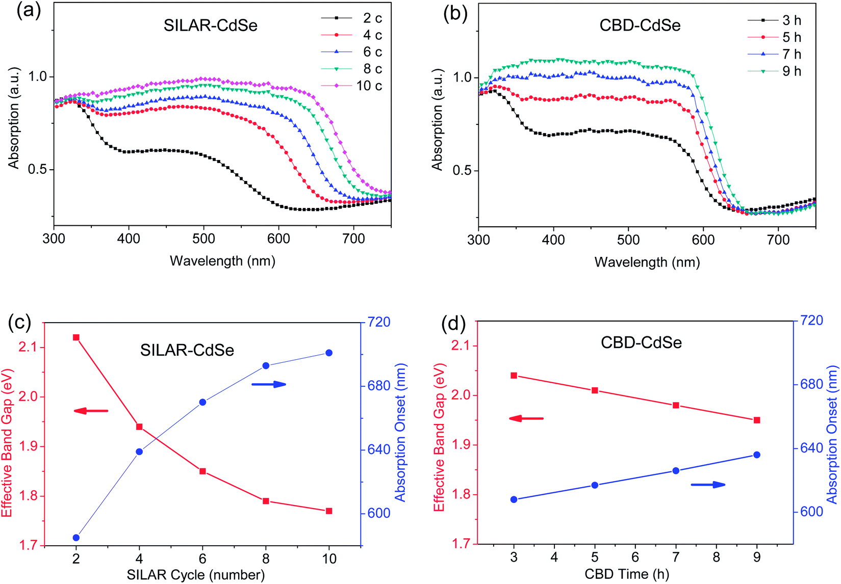 | ||
| Fig. 1 UV-vis absorption spectra of CdSe QD sensitized TiO2 mesoporous films prepared by (a) SILAR for various cycles and (b) CBD for different times, respectively, and the estimated effective band gaps and absorption onsets depending on (c) SILAR cycle and (d) CBD time, determined by the corresponding UV-vis absorption spectra. | ||
The light harvesting capability, as one of the key functional properties of a QD-sensitized film, can be evaluated using the UV-vis absorption spectrum, which highlights two important features: (1) the particle size of QDs reflected by the absorption range, and (2) the amount of QDs loaded determined by the absorbance. Through a careful examination of the absorption spectra of SILAR- and CBD-CdSe films, the clear differences need to be elaborated here. Firstly, it was more facile for SILAR-CdSe films to exhibit a pronounced absorption red shift compared to CBD-CdSe films, which suggested a larger crystalline size for QDs prepared by SILAR. Secondly, comparatively stronger absorbances were more likely to be reached for CBD-CdSe films in comparison with SILAR-CdSe films, indicating a relatively higher QD loading delivered by CBD.
The photovoltaic properties of CdSe QDSCs based on SILAR and CBD are carefully examined, and the corresponding J–V characteristics under the illumination of one sun (AM 1.5, 100 mW cm−2) are presented in panels (a) and (b) of Fig. 2 for SILAR- and CBD-CdSe QDSCs, respectively. For clear illustration, photovoltaic parameters (i.e., PCE, Jsc, Voc and FF) depending on the SILAR cycle and CBD time are plotted in Fig. 2c and d. It is noteworthy that, for each device studied in this paper, at least three identical samples have been fabricated to check the reproducibility of cell performance. As shown in the plotted histograms, the performance of a QDSC was very much dependent on the deposition parameters for both strategies, and the PCE first increased and then decreased with increasing the SILAR cycle and CBD time to deposit CdSe QDs. Specifically, it is easy to understand that a small amount of QDs incorporated on the TiO2 film would result in a small photocurrent density, along with a low PCE. However, an overload of QDs might also lead to a poor cell performance, possibly for the reason of blocking of the mesopores, which gave rise to a decrease of the QD/electrolyte contact area and unfavorable electron transport at the TiO2/QDs/electrolyte interface.16,36 This explains the fact that, although the QD loading would further increase, the cell performance deteriorated along with the overextended SILAR cycle (>6) or CBD time (>5 h).
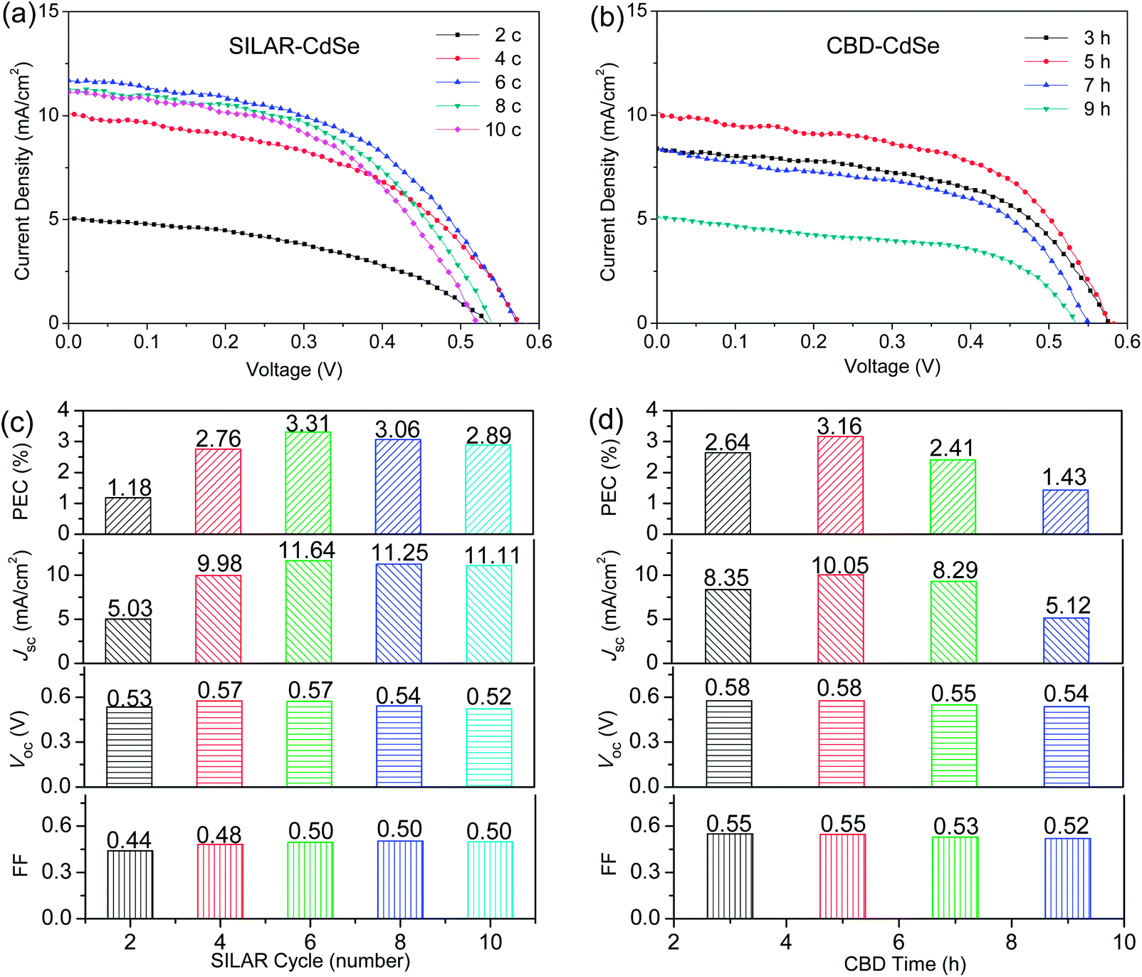 | ||
| Fig. 2 J–V characteristics of CdSe QDSCs prepared by (a) SILAR and (b) CBD, and photovoltaic parameters (PCE, Jsc, Voc and FF) depending on (c) SILAR cycle and (d) CBD time, respectively, measured under the illumination of one sun (AM 1.5, 100 mW cm−2). | ||
Optimized PCEs of 3.31% and 3.16% were achieved for SILAR- and CBD-CdSe QDSCs, respectively. In order to carefully compare the differences of the two deposition techniques, we take a look at each photovoltaic parameter separately. On one hand, as for Jsc, a highest value of 11.64 mW cm−2 could be obtained for the SILAR-CdSe cell (SILAR cycle = 6), a little higher than that of the highest one of 10.05 mW cm−2 for the CBD-CdSe cell (CBD time = 5 h). Evidently, as the photocurrent was proportional to the amount of photons captured, the slightly larger Jsc should be directly associated with the broader light absorption range of QDs for the SILAR-CdSe cell, compared to that of the CBD-CdSe cell, although the amount of QD loading might be comparatively smaller. On the other hand, higher Voc and FF values were systematically observed for CBD-CdSe cells compared to SILAR-CdSe cells, taking into consideration the value variation depending on the deposition parameters. For instance, the FF of CBD-CdSe cells lies between 0.52 and 0.55, higher than the values distributed in the range of 0.44 to 0.50 for SILAR-CdSe cells. As the identical TiO2 mesoporous film, electrolyte and counter electrode were employed for cell fabrication, the obvious differences in photovoltaic behavior of SILAR- and CBD-CdSe cells unequivocally resulted from the different deposition techniques.
A pre-assembled seed layer of CdS QDs prior to CdSe deposition has been extensively reported to improve the cell performance.8,10,18 Several possibilities have been proposed to explain the complementary effect in the literatures, including the passivation effect of CdS on the TiO2 surface, the growth of different natures of CdSe (or TiO2/CdSe junction), the formation of stepwise band-edge levels facilitating electron injection and so forth.10,18,37 Here, we will not belabor the particular effects of the CdS seed layer too much, as they are beyond the research scope of this study. A CdS QD seed layer prepared by SILAR for 4 cycles was employed in this work and verified to improve the cell performance.
Fig. 3a presents the UV-vis absorption spectra of CdS seeded SILAR-CdSe (SILAR cycle = 6) and CBD-CdSe (CBD time = 3 h) films, denoted as CdS/SILAR-CdSe and CdS/CBD-CdSe, respectively. In the presence of a SILAR-CdS seed layer, the growth of CdSe was greatly enhanced as demonstrated by the higher absorbances, compared to those of the corresponding pure CdSe QD sensitized films. Moreover, the CdS/SILAR-CdSe film exhibited a broader absorption range with an absorption onset at a wavelength of ca. 667 nm, longer than that of ca. 636 nm for the CdS/CBD-CdSe film (as illustrated in Fig. S1c†), while the absorbance of the CdS/CBD-CdSe film was higher than that of the CdS/SILAR-CdSe film, implying the larger amount of QD loading, similar to the case for pure CdSe sensitized films as demonstrated in Fig. 1a and b. Another point of particular interest is the CB lineup affected by the QD size. In consideration of the smaller QD size of CdS/CBD-CdSe suggested by the shorter wavelength of the absorption onset in comparison with CdS/SILAR-CdSe, the facilitated electron injection from the CB of QDs to the CB of TiO2 and the reduced back charge transfer might be achieved, arising from its higher CB edge, as illustrated in Scheme S2.† Although the exact CB lineups of QDs are not very clear in our case because of the high pH of the polysulfide electrolyte, which has been reported to make the TiO2 bands shift negatively to a greater extent than the corresponding shifts of CdS or CdSe QDs,18 it can be inferred that a larger offset of the CB of CdSe with respect to the CB of TiO2 will render the electron injection rather facile, while a smaller offset probably leads to the recombination of photo-generated carriers.
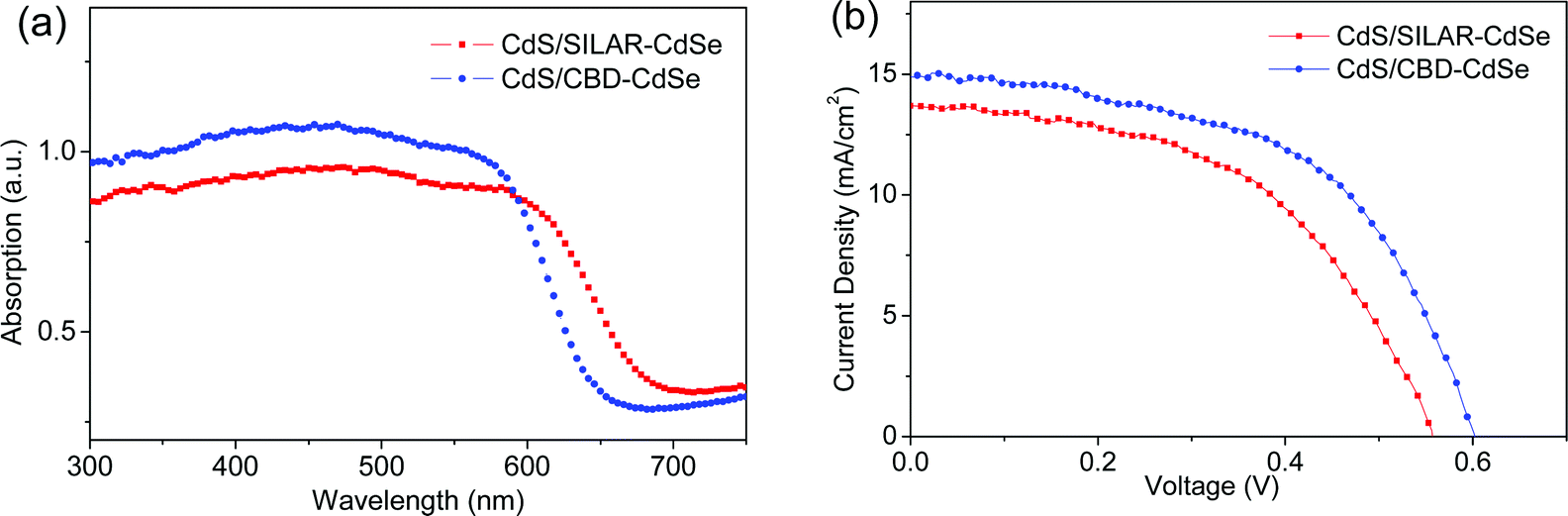 | ||
| Fig. 3 (a) UV-vis absorption spectra of CdS seeded SILAR- and CBD-CdSe electrodes, and (b) J–V characteristics of CdS seeded SILAR- and CBD-CdSe QDSCs measured under the illumination of one sun (AM 1.5, 100 mW cm−2). | ||
The photovoltaic characteristics of CdS seeded SILAR- and CBD-CdSe QDSCs measured under the illumination of one sun (AM 1.5, 100 mW cm−2) are compared in Fig. 3b and the extracted parameters (i.e., Jsc, Voc, FF and PCE) are summarized in Table 1. As shown, a Jsc of 13.64 mA cm−2, a Voc of 0.56 V, a FF of 0.51, and a PCE of 3.89% were achieved for the CdS/SILAR-CdSe cell, while the CdS/CBD-CdSe cell delivered a Jsc of 14.98 mA cm−2, a Voc of 0.60 V, and a FF of 0.54, leading to a PCE of 4.85%. Two performance features are worth mentioning here: firstly, a larger Jsc was reached for the CdS seeded CBD cell than that of the CdS seeded SILAR cell. It is well known that Jsc relies not only on the photocarrier generation process based on light harvest capability but also on a process after photocarrier generation, i.e., electron injection. On one hand, as presented in the absorption spectra, the CdS/CBD-CdSe film exhibited much more efficient photon capturing than that of the CdS/SILAR-CdSe film, although the red-shifted absorption edge of the CdS/SILAR-CdSe film could make up for a somewhat weaker light harvest capability. The stronger absorbance of the CdS/CBD-CdSe film indicated a higher QD loading delivered by CdS seeded CBD. On the other hand, a more facile electron injection achieved in view of the higher CB edge of CdS/CBD-CdSe QDs, compared to that of CdS/SILAR-CdSe QDs, would result in a more efficient photon to electron quantum yield. Therefore, CdS/CBD-CdSe cells delivered a larger Jsc than that of CdS/SILAR-CdSe cells. Secondly, particular attention is paid to Voc and FF. Compared to CdS seeded SILAR, the CdS seeded CBD consistently delivered higher and more reproducible Voc and FF. As Voc and FF are systematically correlated with the charge recombination processes in the solar device,29,38 it might be inferred that lower charge recombination would occur for the CdS/CBD-CdSe cell in comparison with the CdS/SILAR-CdSe cell, which might have resulted from the well-distributed CBD grown CdSe QDs. In order to validate our conjecture on the different photovoltaic features for CdS seeded SILAR- and CBD-CdSe cells, we resorted to microcosmic examinations for further reasonable explanations, as discussed below.
| Cell | J sc (mA cm−2) | V oc (V) | FF | PCE (%) |
|---|---|---|---|---|
| a The standard deviation of the photovoltaic characteristics is based on the data of three cells. | ||||
| CdS/SILAR-CdSe | 13.64 (±0.20) | 0.56 (±0.01) | 0.51 (±0.01) | 3.89 (±0.20) |
| CdS/CBD-CdSe | 14.98 (±0.20) | 0.60 (±0.01) | 0.54 (±0.01) | 4.85 (±0.20) |
The mesoporous structure of TiO2 films, shown in Fig. 4a, favors the penetration of the precursor solutions. As is well-known, for absorber (i.e., dye or QD) deposition, it is important that the absorber is deposited throughout the porous oxide layer, which is ca. 16 μm as revealed by the cross-sectional view (Fig. 4b) in this case. Therefore, a method that allows the infiltration of the reactants into the film pores is preferentially required. Solution deposition methods, such as SILAR and CBD, are supposed to be ideal for this purpose. Fig. 4c compares the EDX spectra based on the film surfaces for CdS seeded SILAR-CdSe and CBD-CdSe electrodes, which confirms the successful deposition of CdS and CdSe. The atomic ratios of the elements, listed in the inset of each spectrum, revealed that, compared to SILAR, CBD led to loading of a larger amount of QDs, consistent with the results obtained from the absorption spectra (Fig. 3a) and XPS analysis (Fig. S2†). For microscopically tracing the spatial distribution of CdS and CdSe in the mesoporous film, the elemental mapping technique was employed. The cross-sectional mapping images as presented in Fig. 4d demonstrated that the element distributions of Cd, S and Se were indeed essentially homogeneous throughout the thickness of the mesoporous TiO2 film for both CdS seeded SILAR and CBD, as we had expected.
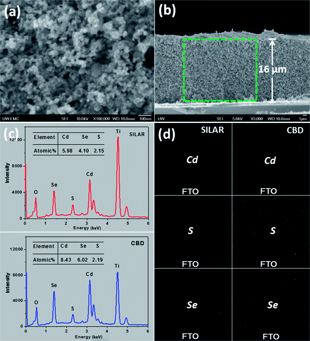 | ||
| Fig. 4 SEM images of (a) top view and (b) cross-sectional view of a bare TiO2 mesoporous film, (c) EDX spectra based on the film surface and (d) element distribution maps of Cd, S and Se along the cross-section for CdS seeded SILAR-CdSe and CBD-CdSe films. | ||
The deposition status of QDs on TiO2 films can be microscopically revealed by TEM images as shown in Fig. 5. Compared to the images of pure TiO2 nanoparticles (Fig. 5a and d), the images of TiO2 nanoparticles loaded with QDs (Fig. 5b and c) clearly indicated the successful deposition of QDs, which could be further confirmed as TiO2/CdS/CdSe structures by HRTEM images (Fig. 5e and f). It is apparent that the deposition status of CdS/SILAR-CdSe on the TiO2 surface differs from that of CdS/CBD-CdSe. The observations manifest that CBD can ensure the preferential growth of QDs on the TiO2 surface, forming a full conformal coverage of the “thin QD layer” coated continuously on the surface of TiO2, while SILAR produces separated “small QD particles” distributed on TiO2, as has also been previously reported in the literature.23,25,39,40 Presumably, the success in achieving a full conformal coverage and high loading of QDs for the CdS/CBD-CdSe electrode would lead to an interfacial structure with superior ability to inhibit the charge recombination at the TiO2/electrolyte interface, thus contributing for the improvements of Voc and FF of the corresponding solar cells. In contrast, although it was also easy for the CdS/SILAR-CdSe electrode to load a certain amount of QDs on TiO2 judging from the color change, the discontinuous distribution and imperfect anchorage of QDs might give rise to interface charge recombination, which would inevitably worsen the cell performance. The explanations coincide with the photovoltaic behaviors of CdS seeded SILAR- and CBD-CdSe cells.
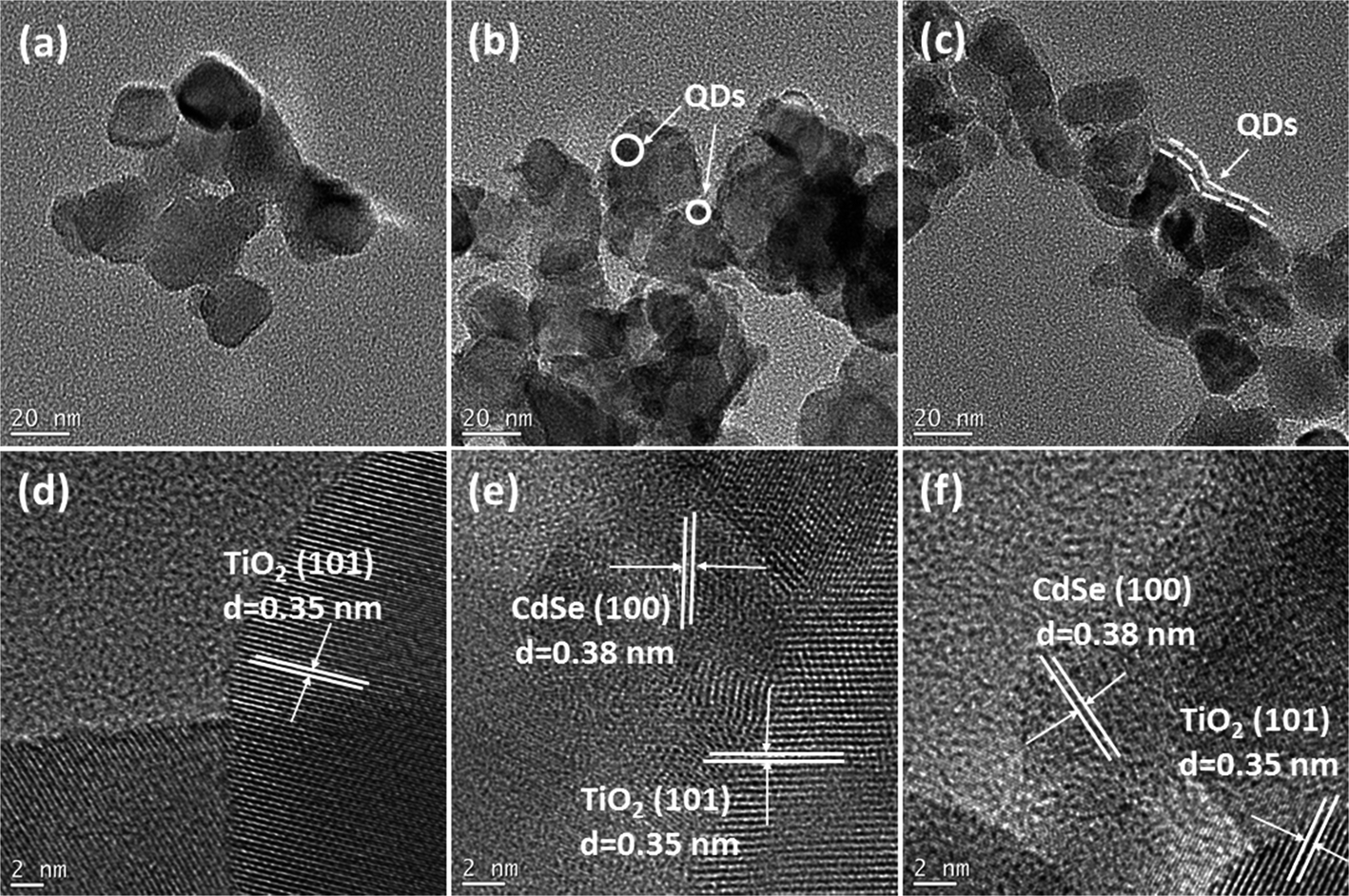 | ||
| Fig. 5 TEM and HRTEM images of TiO2 nanoparticles (a and d) before QDs deposition, and after CdSe QDs deposited by CdS seeded (b and e) SILAR and (c and f) CBD. | ||
The significant influences of QD deposition status on the interfacial charge transfer and recombination are illustrated in Fig. 6. As demonstrated in panel (a), under illumination, photons are harvested by the QD absorbers, generating electron–hole pairs that are quickly separated. The electrons excited to the CB of QDs inject into the CB of TiO2, and then are collected by the FTO substrate, while the holes left in the QDs are reduced by S2− ions in the electrolyte. Particularly, besides the charge transfer processes, there also exist some charge recombination pathways as marked in the schematic diagram:14,41kb and kr represent the back reaction of the injected electrons in the CB of QDs and TiO2 with Sn2− ions in the electrolyte and the recombination of these electrons with holes remaining in the VB of QDs, respectively. Among all these pathways, the back electron injection from TiO2 to the electrolyte dominates the recombination processes in view of the highly efficient charge separation of QDs.14,42 A full conformal coverage of the QD layer on TiO2 will be effective in preventing the back reaction of electrons in the CB of TiO2 with Sn2−. Schematic diagrams shown in panel (b) highlight the differences of CdSe QD deposition between CdS seeded SILAR and CBD, on the basis of TEM observations. Apparently, in comparison with CdS/SILAR-CdSe, the CdS/CBD-CdSe electrode provides better blockage of electron re-injection from TiO2 back into the electrolyte, which will undoubtedly suppress the charge recombination. In addition, it is worth mentioning that the QDs layer plays an active role in the charge transfer and recombination processes in QDSCs, perhaps by forming an electron transport channel along QDs, a situation that is different from that in typical DSCs.29,43 S. H. Yang's group has also reported that, even for the same TiO2 mesoporous films employed, the compact QD layer not only helps to suppress recombination but also gives rise to enhanced charge transport in a solar device.29
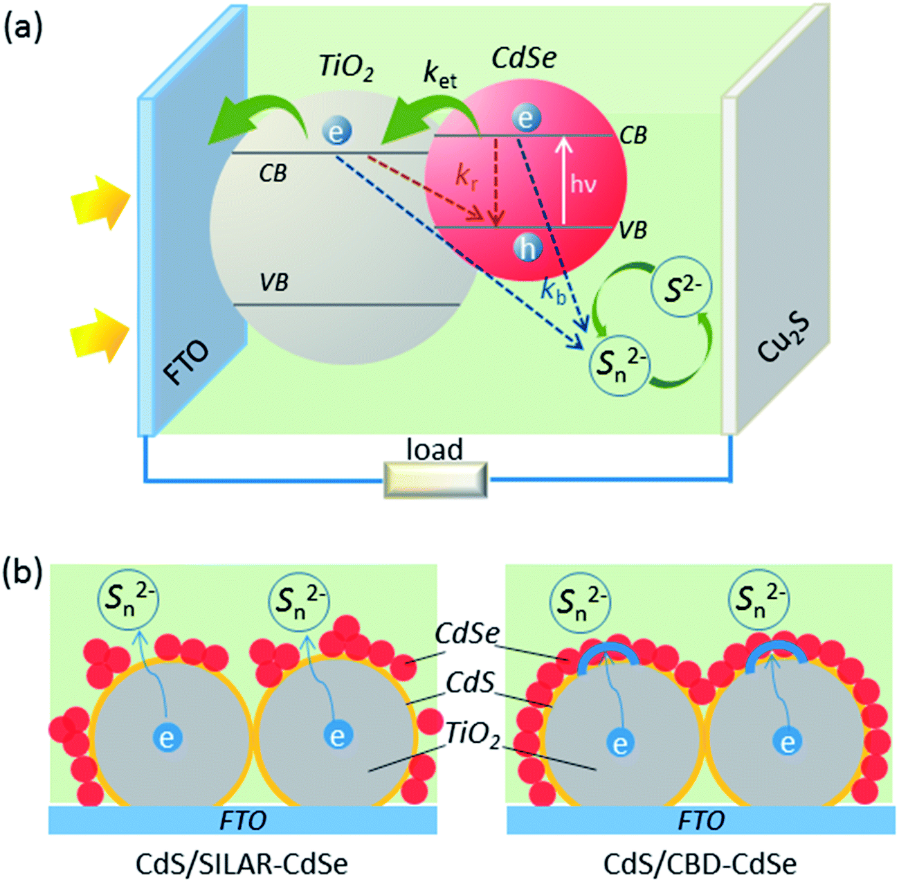 | ||
| Fig. 6 Schematic diagrams (a) illustrating the electron transfer (ket) from CdSe into TiO2 nanoparticles. kb and kr represent the back reaction of the injected electrons in the CB of QDs and TiO2 with Sn2− ions in the electrolyte and the recombination of these electrons with holes remaining in the VB of QDs, respectively; (b) highlighting the differences of CdSe QD deposition between CdS seeded SILAR and CBD. | ||
To evaluate the resistance distributions and charge recombination processes in the solar device, especially at interfaces, EIS measurements have been carried out. Fig. 7a and b show the impedance spectra of CdS seeded SILAR- and CBD-CdSe cells recorded under dark conditions at an applied forward bias of −0.6 V. The EIS curves were fitted in terms of the equivalent circuit depicted in the inset of Fig. 7a. Rs accounts for the sheet resistance of FTO and the contact resistance between FTO and TiO2, and two typical semicircles in the Nyquist plot of QDSCs corresponded to the redox reaction at the counter electrode/electrolyte interface at high frequencies (R1, smaller semicircle), and the electron transfer at the TiO2/QDs/electrolyte interface at medium frequencies (R2, bigger semicircle), respectively.29,42,44,45 The fitting results of Rs, R1 and R2 for QDSCs based on EIS measurements are presented in Table 2. In consideration of the same counter electrode and electrolyte employed in our experiments, R1 exhibits no apparent differences for CdS seeded SILAR- and CBD-CdSe cells as shown in Fig. 7a; while for our interest, we would like to draw attention to the most conspicuous difference between the two cells, i.e., R2, which reflects the charge recombination corresponding to the kb and kr processes illustrated in Fig. 6a. The R2 of the CdS/CBD-CdSe cell is 93.3 Ω, which is more than twice that of the CdS/SILAR-CdSe cell (40.2 Ω). This fact revealed that, compared to CdS/SILAR-CdSe, electrons in the CdS/CBD-CdSe photoanode are more difficult to recombine with the electrolyte redox couple (S2−/Sn2−) in view of the higher R2 value. As the same counter electrode, electrolyte and TiO2 film were employed in both cells, the value difference of R2 should be closely associated with the deposition status of QDs on the TiO2 surface, which could give rise to different charge transport and recombination characteristics. Evidently, the full conformal coverage of QDs on TiO2 achieved by the CdS seeded CBD technique leads to the reduction of the contact area of TiO2 with the electrolyte, thus leading to the suppressed charge recombination and enhanced electron transport in the device. Fig. 7b shows the bode plots of the impedance spectra. The electron lifetime (τn) in the TiO2 can be evaluated by the peak frequency at the minimum phase angle in the Bode plot based on the following equation:45–47
 | (2) |
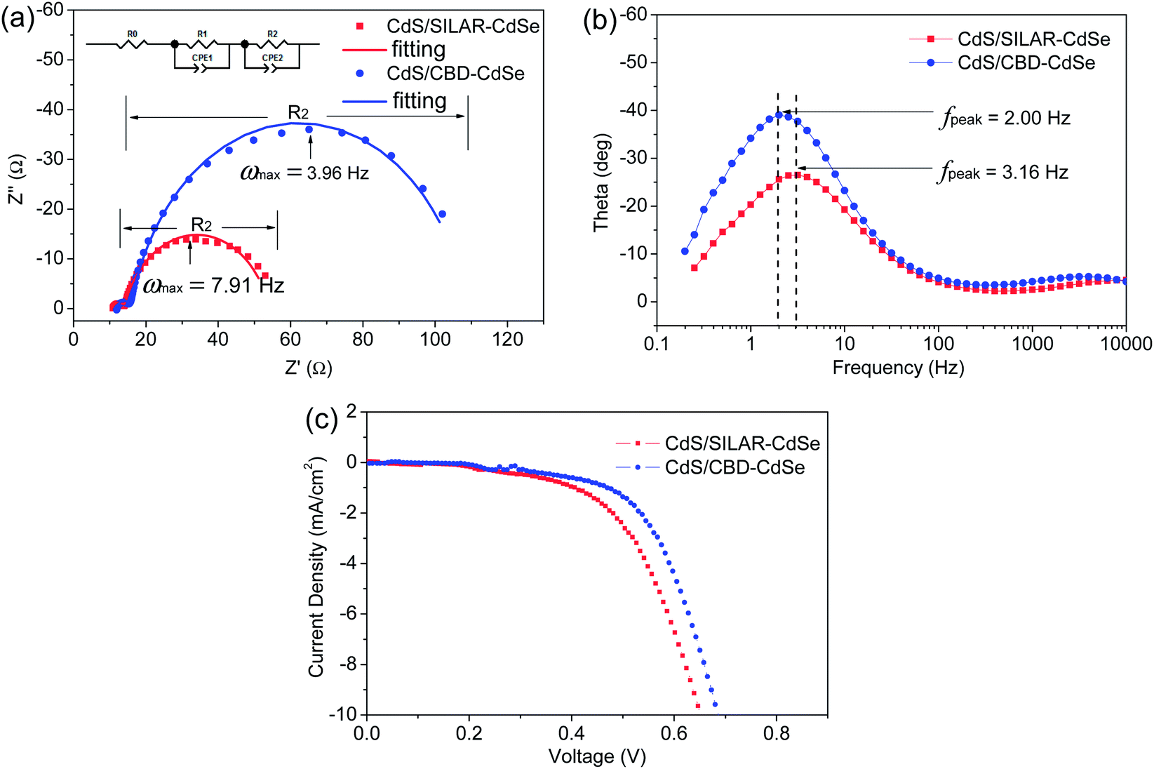 | ||
| Fig. 7 (a) Nyquist plots and (b) Bode plots of EIS spectra of CdS seeded SILAR- and CBD-CdSe cells recorded under dark conditions at an applied forward bias of −0.6 V, and (c) J–V characteristics of CdS seeded SILAR- and CBD-CdSe QDSCs measured under dark conditions. | ||
| Sample | R s (Ω) | R 1 (Ω) | R 2 (Ω) | τ n (ms) |
|---|---|---|---|---|
| CdS/SILAR-CdSe | 11.26 | 3.2 | 40.2 | 50.4 |
| CdS/CBD-CdSe | 11.92 | 3.9 | 93.3 | 79.6 |
The estimated electron lifetime of the CdS/CBD-CdSe cell is up to 79.6 ms, much longer than that of 50.4 ms for the CdS/SILAR-CdSe cell. Apparently, the long lifetime of the charge carrier implies a suppressed charge recombination, and ensures the efficient collection of electrons at the FTO substrate.
Based on the above discussions, it is concluded that CdS/CBD-CdSe has superior ability, compared to CdS/SILAR-CdSe, to inhibit the charge recombination from TiO2 back to the redox couple (S2−/Sn2−) in the electrolyte, arising from the full conformal coverage of QDs on the TiO2 surface. The suppression of interfacial charge recombination results in a high Voc and a large FF. Moreover, the inference is further supported by the J–V characteristics measured under dark conditions (shown in Fig. 7c), which shows a smaller dark current for the CdS/CBD-CdSe cell than that of the CdS/SILAR-CdSe cell.
4. Conclusions
The present work has demonstrated the appreciable influences of deposition strategies, i.e., SILAR and CBD, on the assembly of QDs on mesoporous films and the performance of the resultant QDSCs. The photovoltaic characteristics of CdSe sensitized TiO2 solar cells vary considerably depending on the synthesis strategy and deposition parameters. Optical measurement and microcosmic examination of the QD-deposited films revealed that, compared to CdS seeded SILAR that is only capable of less than full coverage, CdS seeded CBD could deliver a high loading and full conformal coverage of CdSe QDs on TiO2, which contributed to the improvement of cell performance. On one hand, a high loading of QDs secures efficient photon capturing, benefitting the increase of Jsc; on the other hand, the full conformal coverage of QDs suppresses the interfacial charge recombination, so as to enhance Voc and FF. Eventually, an overall PCE of 4.85% has been reached for CdS/CBD-CdSe cells, which remarkably outperformed CdS/SILAR-CdSe cells (PCE = 3.89%). This work emphasizes the importance of interface engineering in QDSCs and performance improvements are promisingly expected through further optimization and development of manufacturing procedures of solar devices.Acknowledgements
This work was financially supported by the National Natural Science Foundation (NSF) of China (no. 51372061 and 51302057) and the funding provided by the Seed Foundation of Hefei University of Technology (no. 2014HGBZ0334). This work was also supported in part by the National Science Foundation (DMR 1035196) and the University of Washington TGIF grant. R. Zhou also gratefully acknowledges a fellowship from the China Scholarship Council.Notes and references
- I. J. Kramer and E. H. Sargent, Chem. Rev., 2014, 114, 863–882 CrossRef CAS PubMed.
- M. Grätzel, Nat. Mater., 2014, 13, 838–842 CrossRef PubMed.
- Y. Shirasaki, G. J. Supran, M. G. Bawendi and V. Bulović, Nat. Photonics, 2013, 7, 13–23 CrossRef CAS PubMed.
- Z. X. Pan, I. Mora-Seró, Q. Shen, H. Zhang, Y. Li, K. Zhao, J. Wang, X. H. Zhong and J. Bisquert, J. Am. Chem. Soc., 2014, 136, 9203–9210 CrossRef CAS PubMed.
- H. Tada, M. Fujishima and H. Kobayashi, Chem. Soc. Rev., 2011, 40, 4232–4243 RSC.
- P. V. Kamat, K. Tvrdy, D. R. Baker and J. G. Radich, Chem. Rev., 2010, 110, 6664–6688 CrossRef CAS PubMed.
- S. Rühle, M. Shalom and A. Zaban, ChemPhysChem, 2010, 11, 2290–2304 CrossRef PubMed.
- P. K. Santra and P. V. Kamat, J. Am. Chem. Soc., 2012, 134, 2508–2511 CrossRef CAS PubMed.
- V. Gonzalez-Pedro, X. Xu, I. Mora-Seró and J. Bisquert, ACS Nano, 2010, 4, 5783–5790 CrossRef CAS PubMed.
- Y. L. Lee and Y. S. Lo, Adv. Funct. Mater., 2009, 19, 604–609 CrossRef PubMed.
- J. Wang, I. Mora-Seró, Z. X. Pan, K. Zhao, H. Zhang, Y. Y. Feng, G. Yang, X. H. Zhong and J. Bisquert, J. Am. Chem. Soc., 2013, 135, 15913–15922 CrossRef CAS PubMed.
- Z. X. Pan, K. Zhao, J. Wang, H. Zhang, Y. Y. Feng and X. H. Zhong, ACS Nano, 2013, 7, 5215–5222 CrossRef CAS PubMed.
- J. J. Tian, E. Uchaker, Q. F. Zhang and G. Z. Cao, ACS Appl. Mater. Interfaces, 2014, 6, 4466–4472 CAS.
- J. J. Tian, Q. F. Zhang, L. L. Zhang, R. Gao, L. F. Shen, S. G. Zhang, X. H. Qu and G. Z. Cao, Nanoscale, 2013, 5, 936–943 RSC.
- R. Zhou, Q. F. Zhang, E. Uchaker, J. L. Lan, M. Yin and G. Z. Cao, J. Mater. Chem. A, 2014, 2, 2517–2525 CAS.
- R. Zhou, Q. F. Zhang, J. J. Tian, D. Myers, M. Yin and G. Z. Cao, J. Phys. Chem. C, 2013, 117, 26948–26956 CAS.
- R. Zhou, Q. F. Zhang, E. Uchaker, L. Yang, N. Q. Yin, Y. H. Chen, M. Yin and G. Z. Cao, Electrochim. Acta, 2014, 135, 284–292 CrossRef CAS PubMed.
- O. Niitsoo, S. K. Sarkar, C. Pejoux, S. Rühle, D. Cahen and G. Hodes, J. Photochem. Photobiol., A, 2006, 181, 306–313 CrossRef CAS PubMed.
- H. Lee, W. T. Sun, Y. Yu, H. Y. Pan, X. F. Gao, Q. Chen and L. M. Peng, J. Am. Chem. Soc., 2008, 130, 1124–1125 CrossRef PubMed.
- I. Robel, V. Subramanian, M. Kuno and P. V. Kamat, J. Am. Chem. Soc., 2006, 128, 2385–2393 CrossRef CAS PubMed.
- T. L. Li, Y. L. Lee and H. Teng, Energy Environ. Sci., 2012, 5, 5315–5324 CAS.
- M. K. Wang, P. Chen, D. R. Gamelin, S. M. Zakeeruddin, M. Grätzel and M. K. Nazeeruddin, Nano Lett., 2009, 9, 4221–4227 CrossRef PubMed.
- A. Braga, S. Giménez, I. Concina, A. Vomiero and I. Mora-Seró, J. Phys. Chem. Lett., 2011, 2, 454–460 CrossRef CAS.
- A. Tubtimtae, K. L. Wu, H. Y. Tung, M. W. Lee and G. J. Wang, Electrochem. Commun., 2010, 12, 1158–1160 CrossRef CAS PubMed.
- J.-W. Lee, D.-Y. Son, T. K. Ahn, H.-W. Shin, I. Y. Kim, S.-J. Hwang, M. J. Ko, S. Sul, H. Han and N.-G. Park, Sci. Rep., 2013, 3, 1050 Search PubMed.
- M. A. Hossain, J. R. Jennings, C. Shen, J. H. Pan, Z. Y. Koh, N. Mathews and Q. Wang, J. Mater. Chem., 2012, 22, 16235–16242 RSC.
- J. J. Tian, L. L. Lv, C. B. Fei, Y. J. Wang, X. G. Liu and G. Z. Cao, J. Mater. Chem. A, 2014, 2, 19653–19659 CAS.
- S. Mathew, A. Yella, P. Gao, R. Humphry-Baker, B. F. E. Curchod, N. Ashari-Astani, I. Tavernelli, U. Rothlisberger, M. K. Nazeeruddin and M. Grätzel, Nat. Chem., 2014, 6, 242–247 CrossRef CAS PubMed.
- K. Y. Yan, W. Chen and S. H. Yang, J. Phys. Chem. C, 2013, 117, 92–99 CAS.
- H. J. Lee, D.-Y. Kim, J.-S. Yoo, J. Bang, S. Kim and S.-M. Park, Bull. Korean Chem. Soc., 2007, 28, 6 Search PubMed.
- D. J. Norris, K. S. Leschkies, R. Divakar, J. Basu, E. EnachePommer, J. E. Boercker, C. B. Carter, U. R. Kortshagen and E. S. Aydil, Nano Lett., 2007, 7, 1793–1798 CrossRef PubMed.
- S. Gimenez, I. Mora-Seró, L. Macor, N. Guijarro, T. LanaVillarreal, R. Gomez, L. J. Diguna, Q. Shen, T. Toyoda and J. Bisquert, Nanotechnology, 2009, 20, 295204 CrossRef PubMed.
- V. González-Pedro, C. Sima, G. Marzari, P. P. Boix, S. Giménez, Q. Shen, T. Dittrich and I. Mora-Seró, Phys. Chem. Chem. Phys., 2013, 15, 13835–13843 RSC.
- J. J. Tian, R. Gao, Q. F. Zhang, S. G. Zhang, Y. W. Li, J. L. Lan, X. H. Qu and G. Z. Cao, J. Phys. Chem. C, 2012, 116, 18655–18662 CAS.
- R. Gao, L. Wang, Y. Geng, B. Ma, Y. Zhu, H. Dong and Y. Qiu, J. Phys. Chem. C, 2011, 115, 17986–17992 CAS.
- S. C. Lin, Y. L. Lee, C. H. Chang, Y. J. Shen and Y. M. Yang, Appl. Phys. Lett., 2007, 90, 143517 CrossRef PubMed.
- Y.-L. Lee, B.-M. Huang and H.-T. Chien, Chem. Mater., 2008, 20, 6903–6905 CrossRef CAS.
- K. Lee, S. W. Park, M. J. Ko, K. Kim and N.-G. Park, Nat. Mater., 2009, 8, 665–671 CrossRef CAS PubMed.
- H. Lee, H. C. Leventis, S.-J. Moon, P. Chen, S. Ito, S. A. Haque, T. Torres, F. Nüesch, T. Geiger, S. M. Zakeeruddin, M. Grätzel and M. K. Nazeerruddin, Adv. Funct. Mater., 2009, 19, 2735–2742 CrossRef CAS PubMed.
- H. J. Lee, J. Bang, J. Park, S. Kim and S.-M. Park, Chem. Mater., 2010, 22, 5636–5643 CrossRef CAS.
- I. Mora-Seró, S. Giménez, F. Fabregat-Santiago, R. Gómez, Q. Shen, T. Toyoda and J. Bisquert, Acc. Chem. Res., 2009, 42, 1848–1857 CrossRef PubMed.
- X. Y. Yu, J. Y. Liao, K. Q. Qiu, D. B. Kuang and C. Y. Su, ACS Nano, 2011, 5, 9494–9500 CrossRef CAS PubMed.
- I. Hod, V. González-Pedro, Z. Tachan, F. Fabregat-Santiago, I. Mora-Seró, J. Bisquert and A. Zaban, J. Phys. Chem. Lett., 2011, 2, 3032–3035 CrossRef CAS.
- N. Koide, A. Islam, Y. Chiba and L. Y. Han, J. Photochem. Photobiol., A, 2006, 182, 296–305 CrossRef CAS PubMed.
- Q. Wang, J.-E. Moser and M. Grätzel, J. Phys. Chem. B, 2005, 109, 14945–14953 CrossRef CAS PubMed.
- R. Kern, R. Sastrawan, J. Ferber, R. Stangl and J. Luther, Electrochim. Acta, 2002, 47, 4213–4225 CrossRef CAS.
- J. J. Tian, Q. F. Zhang, E. Uchaker, R. Gao, X. H. Qu, S. G. Zhang and G. Z. Cao, Energy Environ. Sci., 2013, 6, 3542–3547 CAS.
Footnote |
| † Electronic supplementary information (ESI) available: Schematic illustrations of the typical procedures for SILAR and CBD processes to deposit CdSe QDs. (Ahυ)2vs. hυ plots for determining the absorption onsets, effective band gap and band gap shift of CdSe QDs obtained. Scheme illustrating the dependence of energy difference between the CBs on the QD size for CdS seeded SILAR-CdSe and CBD-CdSe, and the electron transfer from CdSe QDs with different sizes into TiO2. Experimental details and typical survey of XPS measurements and surface compositions of CdS/SILAR-CdSe and CdS/CBD-CdSe sensitized TiO2 electrodes obtained from XPS analysis. See DOI: 10.1039/c5ta01461a |
| This journal is © The Royal Society of Chemistry 2015 |