
 Open Access Article
 This Open Access Article is licensed under a
 Creative Commons Attribution 3.0 Unported Licence
Morphology and local electrical properties of PTB7:PC71BM blends†
Alexander
Alekseev
*ab,
Gordon J.
Hedley
c,
Alaa
Al-Afeef
a,
Oleg A.
Ageev
d and
Ifor D. W.
Samuel
*c
aMCMP, School of Physics and Astronomy, Kelvin Nanocharacterization Centre, University of Glasgow, University Avenue, Glasgow, G128QQ, UK. E-mail: alalrus@gmail.com
bKazan Federal University, Kremlevskaya str., 18, Kazan, 420000, Russia
cOrganic Semiconductor Centre, SUPA, School of Physics and Astronomy, University of St Andrews, North Haugh, St Andrews, Fife KY16 9SS, UK. E-mail: idws@st-andrews.ac.uk
dInstitute of Nanotechnologies, Electronics and Electronic Equipment Engineering, Southern Federal University, Shevchenko str., 2, Taganrog, 347928, Russia
First published on 12th March 2015
Abstract
The power conversion efficiency of single layer organic solar cells can approach 10% with blends such as the polymer PTB7 and the fullerene derivative PC71BM. Here the detailed structure of PTB7:PC71BM blends deposited with and without addition of diiodooctane is studied by transmission electron microscopy and scanning probe microscopy. The details of bulk structure, such as the thickness of the layer covering fullerene domains and the grain structure of the film are examined. We find that fullerene-rich domains can be near the surface of the film or buried deeper, near the substrate. The local electrical properties of these blends are studied by conductive atomic force microscopy for different configurations of electrodes. Different power conversion efficiencies of blends with and without diiodooctane are explained in terms of local photoconductive properties.
Introduction
Organic photovoltaic (OPV) solar cells, which can be made with simple manufacturing processes, borrowing deposition techniques from the printing industry such as roll-to-roll and spray coating, are attracting significant research activity in an effort to further improve efficiencies. The performance of OPVs depends critically on the nanoscale organization of the photoactive layer and the overall device architecture.1–3 The highest power conversion efficiencies (PCE) are achieved with the bulk heterojunction approach,1–5 in which a donor and an acceptor are mixed in a thin film. With this approach a large interface between the donor and acceptor materials within the whole volume of the photoactive layer is created, helping exciton dissociation. There are different processes influencing device performance, such as light absorption, exciton generation, dissociation and recombination, charge transport and collection etc. All these processes are strongly influenced by the OPV blend morphology. It is a very challenging task to determine and optimize the morphology of OPV blends to provide the maximum PCE. Recently, a single layer OPV based on a bulk heterojunction of two materials: the polymer PTB7, with alternating units of thieno[3,4-b]thiophene and benzodithiophene, and the fullerene derivative [6,6]-phenyl-C71-butyric acid methyl ester (PC71BM) has attracted the attention of researchers,6 since a very high PCE of 9.2% has been reported for devices based on this blend.7 It was reported that the highest PCE for this blend is achieved when diiodooctane (DIO) is used as an additive to solvent.6,7 Some exploration of the morphology and local properties of PTB7:PC71BM have been published in several recent papers,6,8–12 measured by AFM, SEM, TEM and energy filtered TEM. In AFM work looking with AFM11,12 significant changes of surface morphology after the addition of a few percent of DIO to the solution prior to spin-coating were observed, with large fullerene domains prevented from being formed and instead a homogenously mixed blend created, which is in agreement with TEM data. The SEM data also reveal similar morphology changes after use DIO as additive.12 The use of Scanning Transmission X-ray Microscopy (STXM) allowed for the conclusion that the large domains in the pristine blend (without DIO) are PC71BM-rich.10,11 Only blends with large domains (i.e. without DIO) were investigated by STXM due to the limited resolution of this method. Further details of the morphology of this important blend were discovered by using photoconductive-AFM (PC-AFM) and AFM measurements of a plasma-etched surface which removed a thin surface layer.12 Full understanding, however, of the morphology in the PTB7:PC71BM blend is still lacking, and determining the structure and control of the morphology are very important for future development of commercially successful OPVs. In this work we have used different methods of AFM and TEM to get more detailed and comprehensive information about the local structure, composition and properties of the PTB7:PC71BM blend. The combination of TEM and AFM results is very informative, since complementary data are obtained: the TEM detects a projection of the volume structure, energy filtered TEM can give compositional information and AFM is sensitive to the different surface properties. The results of this work expand the knowledge and understanding of the structure and structure–property relationship of OPV blends.Results and discussion
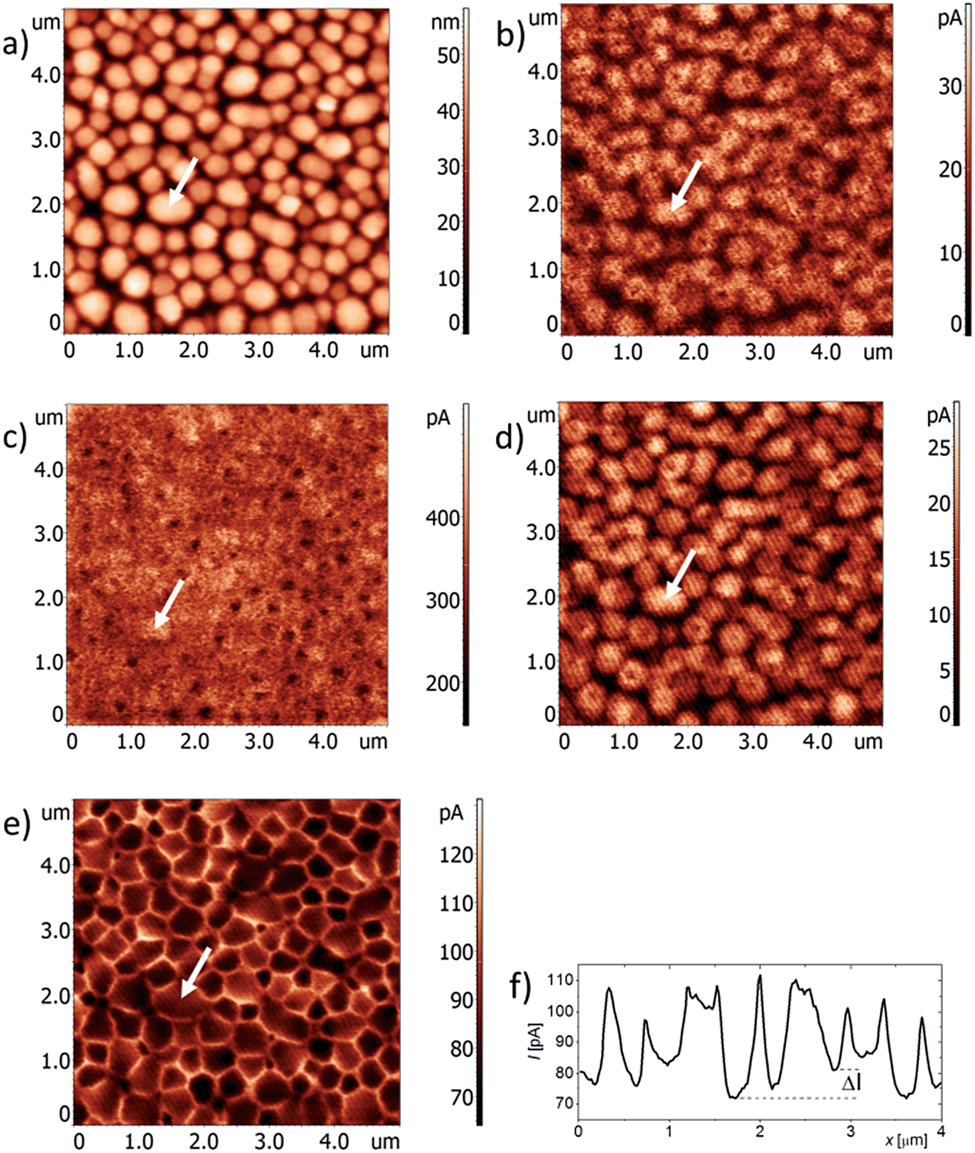
The results described below are related to two samples: PTB7:PC71BM spin-coated from chlorobenzene (Sample 1), and PTB7:PC71BM deposited from chlorobenzene with 3% DIO (Sample 2). First we describe results obtained for Sample 1, which gives additional information about the structure of this blend. AFM, TEM and SEM results of the surface of Sample 1, already reported,6–12 reveal large domains with sizes in the range 200–500 nm. By using AFM we have obtained a similar structure for Sample 1 (Fig. 1a). The average thickness of the PTB7:PC71BM film as measured by AFM across a scratch is around 120 nm. The height variations due to domains are typically less than 30% of the average film thickness. In our recent study we observed a thin skin layer, which covers the domains, by using SEM.12 This skin layer hides a grain structure inside the domains – in this work we will use the nomenclature “particles” to refer to the small pure fullerene spheres 20–60 nm in diameter, and “domains” to refer to agglomerated regions of the particles more than ∼200 nm in diameter.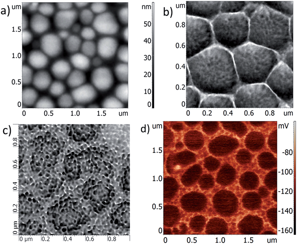 | ||
| Fig. 1 PTB7:PC71BM blend films with no additive (Sample 1): (a) topography measured with AFM, (b) hard-tapping AFM phase image, where repulsive tip-sample forces dominate, enabling observation of a sub-structure inside the domains. (c) After removing a top layer of the sample with plasma etching, AFM phase images show the sub-structure more clearly. (d) KPM image of etched sample. | ||
We were only able to observe below the skin layer by removing it with plasma etching. To ensure that the etching does not alter what we observe we wished to confirm the existence of the particles inside the domains without etching, thus we have applied hard tapping conditions with an AFM on the as-spun film, i.e. with the AFM we are enabling domination of repulsive tip-sample forces. With such a scan (Fig. 1b) we are able to observe a sub-structure inside the domains, strongly resembling the previously imaged particles without even having to remove the skin layer. This gives good evidence that the particles are in fact part of the morphology of the film and not artefacts of the skin removal etch. The bright lines between the domains in the phase image in Fig. 1b are detected because neighbouring domains are placed close to each other and thus the increased tip-sample contact area in such places influences the phase shift.
The observed structure becomes much more pronounced after the removal of the skin layer by plasma etching (Fig. 1c), which indicates that this structure exists inside the film. The thickness of the removed layer by plasma etching is approximately 50 nm, as determined by AFM measurements of a scratched sample. The phase difference between the domains and the matrix in Fig. 1c corresponds to less dissipation in the domains (darker areas with our setup). The different mechanical properties between the domains and the matrix clearly show that there is phase separation inside film. The sizes of particles in both the domains and the matrix are several tens of nanometres, which agrees with the results of photophysical measurements on this sample, which additionally indicated that the particles were composed of pure PC71BM.12 The reproducible removal of material from a polymer sample by plasma etching has been shown before and was used for reconstruction of the volume structure by AFM.13 By observing here that the granular structure inside the film can be detected on the film's surface by using hard tapping conditions with an AFM, and finding the same results using plasma etching, we conclude here that the granular structure inside the film can be detected and it also exists deep inside the photoactive layer.
The use of surface electric potential measurements with AFM (Kelvin Probe Microscopy (KPM)) enables us to distinguish between both components in the film due to their different electronic structure. Fig. 1d demonstrates the distribution of both components in a plasma etched film measured by KPM. The data in Fig. 1d are taken on the surface, which is a few tens nanometers under the original surface. The matrix and domains have a different surface potential, which results in a high contrast KPM image. The inhomogeneous character of the matrix is clearly seen: there are small particles, with diameter of several tens nanometers, which are embedded into a matrix. The particles visible in the domains in Fig. 1b and c are not distinguishable in the KPM image since they have same surface potential and are closely packed (the standard KPM resolution in normal conditions is ∼30–50 nm). Thus, from a comparison of Fig. 1c and d we assume that PC71BM particles form domains surrounded by polymer with inclusion of fullerene particles. A platinum coated probe was used for KPM measurements and the color bar in Fig. 1d shows the surface potential variations relative to the work function of platinum. The absolute value of the surface potential shown in scale bar in Fig. 1d has no real meaning since the surface was irradiated by argon/oxygen plasma and thus any quantitative estimation is not meaningful.
To explore the composition of the domains we have performed Energy Filtered TEM (EFTEM) on Sample 1. The carbon and sulfur maps, (Fig. 2a and b, respectively), demonstrates that the domains are PC71BM-rich, while the matrix mainly consists of the sulfur-containing polymer PTB7, which is consistent with the results obtained by STXM.11 Conventional TEM and EFTEM have been previously used for morphology investigations,6,11 while cross-section of tomography reconstruction made by using EFTEM shows some phase separation inside the volume of photoactive layer.9 Distributions of carbon and sulfur measured by EFTEM and shown in Fig. 2 have inverted contrast in relation to each other, which is a direct consequence of the chemical nature of both components.6
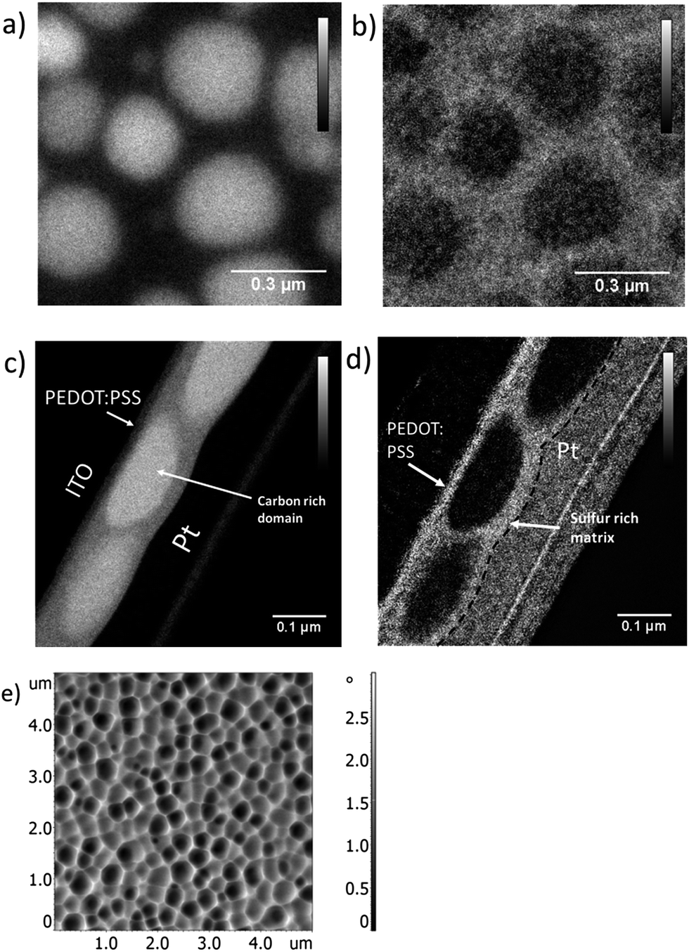 | ||
| Fig. 2 EFTEM images on PTB7:PC71BM without DIO (Sample 1), showing top-down views (top row) and cross-sectional lamella (middle row) of the film. In panels (a) & (c) the carbon distribution is shown, while in (b) & (d) the sulfur distribution. Arrows on the cross-sections indicate the main film stack features, with the glass/ITO/PEDOT:PSS side to the top left and the surface of the film to the bottom right. The scale bars in (c) and (d) are indicative of the observed relative signal strength rather than being absolute. The dashed line in (d) approximately represents the boundary between the electron beam deposited (EBD) platinum and the photoactive layer. (e) AFM phase contrast measurement of the film. Hard tapping enables discrimination between domains close to the surface and those buried deeper in the matrix. | ||
In order to get more detailed information about in-depth structure a cross-section lamella of Sample 1 has been prepared by FIB and investigated by TEM methods. By using CTEM the thin lamella with sample cross-section has been visualized and all sample layers were easily identified (Fig. S1a†). The thickness of the cut lamella is less than 100 nm, which means that the majority of a large domain goes through the lamella thickness. The carbon and sulfur distribution images obtained on the lamella by EFTEM (Fig. 2c and d, respectively) clearly show PC71BM-rich domains embedded into PTB7-rich matrix in the cross-section of the photoactive layer. Combining these results with in-plane images enables us to determine the three dimensional shape of the large domains, finding that they are nearly ellipsoidal in shape, and curve up away from the substrate as well as curving down away from the top of the film. It is also clear that the top skin layer does not have a uniform thickness: on the domain in the top part of Fig. 2c it is very thin, while above the neighbouring domain in the centre of the image the skin layer is quite thick. A similar situation exists on the PEDOT:PSS side of the stack, where the PC71BM domains can either be in close contact with the PEDOT layer or held at some distance away by PTB7-rich material. Typical thicknesses of the skin layer on both sides of the domains are in the range from few nanometres up to 30 nm. The same result was obtained on lamella by conventional TEM (Fig. S1b†).
The weak contrast of the domain in the lower part of Fig. 2c can be explained by fact that only edge of that domain is inside the lamella, and as a result the average concentration of PC71BM is lower when the signal is collected through the film. The same reason can explain the observation of a small sulfur signal coming from lower domain in Fig. 2d. Additionally, a small sulfur signal in the other domains is observed by EFTEM as the intermixing of polymer and PC71BM in domains may occur.11 The large energy filter slit width used by us is responsible for the signal coming from the Pt layer in Fig. 2d, since some background signal may influence the total signal. However, a larger slit width also allows for better signal-to-noise ratio, which is helpful for distinguishing between the domains and the surrounding matrix, and especially for a clearer observation of the thin skin layer. To enable us to distinguish the boundary of the skin layer using the sulfur map in Fig. 2d we use the area with highest signal, with the boundary with the deposited Pt layer marked by a dashed line. It is expected that the presence of a skin layer covering PC71BM-rich domains can significantly influence charge transport in a device. For example, a PTB7-rich skin layer can reduce the efficiency of electron collection, since there is reduced contact between the electron collecting electrode and PC71BM-rich domains.
The variation in the apparent thickness of the skin layer (which can also be viewed as variation in the depth at which fullerene domains are buried) can be explored using hard tapping (free amplitude A0 ∼ 80 nm, set-point to free amplitude ratio Asp/A0 = 0.5) on an AFM equipped with a relatively stiff probe (force constant ∼30 N m−1). In this case a large sample volume is involved in the interaction, which reduces spatial XY resolution, but, at the same time, detection of subsurface structures up to few tens nanometres from the surface becomes possible.14 The domains, which are placed closer to surface and covered by thin skin layer, can be distinguished in the phase image in Fig. 2e, indicating that about half of the domains are close to the surface, and about half are buried deeper within the matrix. We suppose that the skin layer is continues, i.e. no PC71BM-rich domains are exposed to the surface, since the sample surface looks very uniform in both SEM images and in AFM phase images measured with standard conditions (Fig. 1b).11,12 Stiff cores inside domains become visible in the phase image only when a very strong tip-sample interaction is used. It should be noted that the skin layer will influence quantitative results on the domain composition measured by STXM.11 The approximately 70 wt% of PC71BM inside domains measured by STXM is integral value through film thickness and it will be larger if the PTB7 skin layer is taken into account.
We have also used EFTEM tomography15–18 for a complete 3D reconstruction of the structure of Sample 1. Distribution of carbon inside the film after 3D reconstruction is shown in Fig. S2† (see also video in ESI†). The nearly ellipsoidal shape of the PC71BM-rich domains is seen in the tomography image. The cross-sections of tomography images helps to understand the volume structure, however due to the limited range of accessible angles it is not possible to correctly reconstruct the top skin layer by TEM tomography. Therefore, analysis of the lamella cross-section is the only way to get detailed information about the thickness of the skin layer. Investigation of lamella with device cross-section also allows for the utilization of standard high resolution and relatively high contrast TEM methods to study in-depth features.
In the sulfur map shown Fig. 2b it is possible to see a granular structure inside film, with the typical size of several tens nanometres. These particles look similar to that observed by AFM in Fig. 1. In order to have additional evidence of the existence of such particles inside the film, we have utilized the High Angle Annular Dark Field Scanning Transmission Electron Microscopy (HAADF-STEM) regime.19 It has been shown before that the HAADF-STEM regime is a powerful technique for the creation of high contrast images in polymer samples.20,21 The advantages of HAADF-STEM regime, in particular, are: imaging in focus, lack of phase contrast and the high sensitivity of the HAADF detector, which results in high signal-to-noise ratio. It was also shown that HAADF-STEM is able to detect highly electron beam sensitive polymer nanostructures.20 The main source of the contrast obtained by STEM is the density difference between the components of the polymer.20,21 We utilized HAADF-STEM for measurements of pristine blend and the results are shown in Fig. 3. The brighter contrast in the HAADF-STEM image means higher number of electrons collected at detection angles. At the low camera length used in measurements (6 cm) we observe mainly Rutherford scattering. Taking into account that the observed contrast is dependent on density, we conclude that when imaging in dark field conditions brighter areas correspond to PC71BM-rich clusters. This is in agreement with HAADF-STEM results for the MDMO-PPV:PC60BM blend.20,21 The density of observed particles varies: the particles form large domains, which we interpret as PC71BM rich domains described before. Some smooth variations of contrast in Fig. 3 may be related to thickness variations. These smooth variations of contrast overlaps with areas with high concentration of particles, i.e. a higher particle concentration is observed in thicker areas. Between large domains there are small particles with less dense packing. These particles have sizes of several tens nanometres, which is on the same length scale as that of particles in Fig. 1.
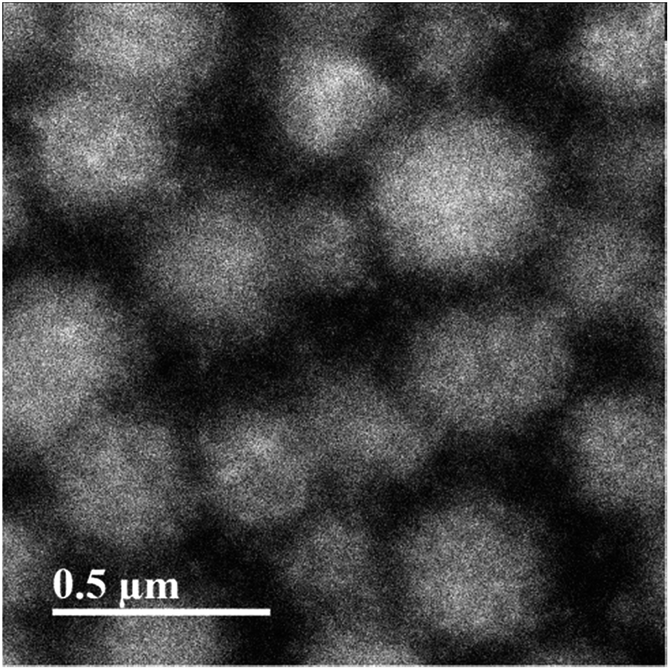 | ||
| Fig. 3 HAADF-STEM image of a film. | ||
Finally, we assume the Sample 1 structure based on all discussed measurements consists of small PC71BM particles, several tens nanometres in diameter, embedded in a PTB7-rich matrix. The large (200–500 nm) domains consist of agglomeration of the small PC71BM particles. The thickness of skin layer above and below domains varies in large range from few nanometres to 30 nm. At the same time exact distribution of PC71BM particles in matrix volume is not clear; more data on film cross-section are required. We believe that there are no visible particles in the domains and matrix in Fig. 2c and d because the measuring conditions (e.g. energy slit) were not optimum to see the very small contrast that will exist between two identical materials (PC71BM) separated by a small amount of PTB7.
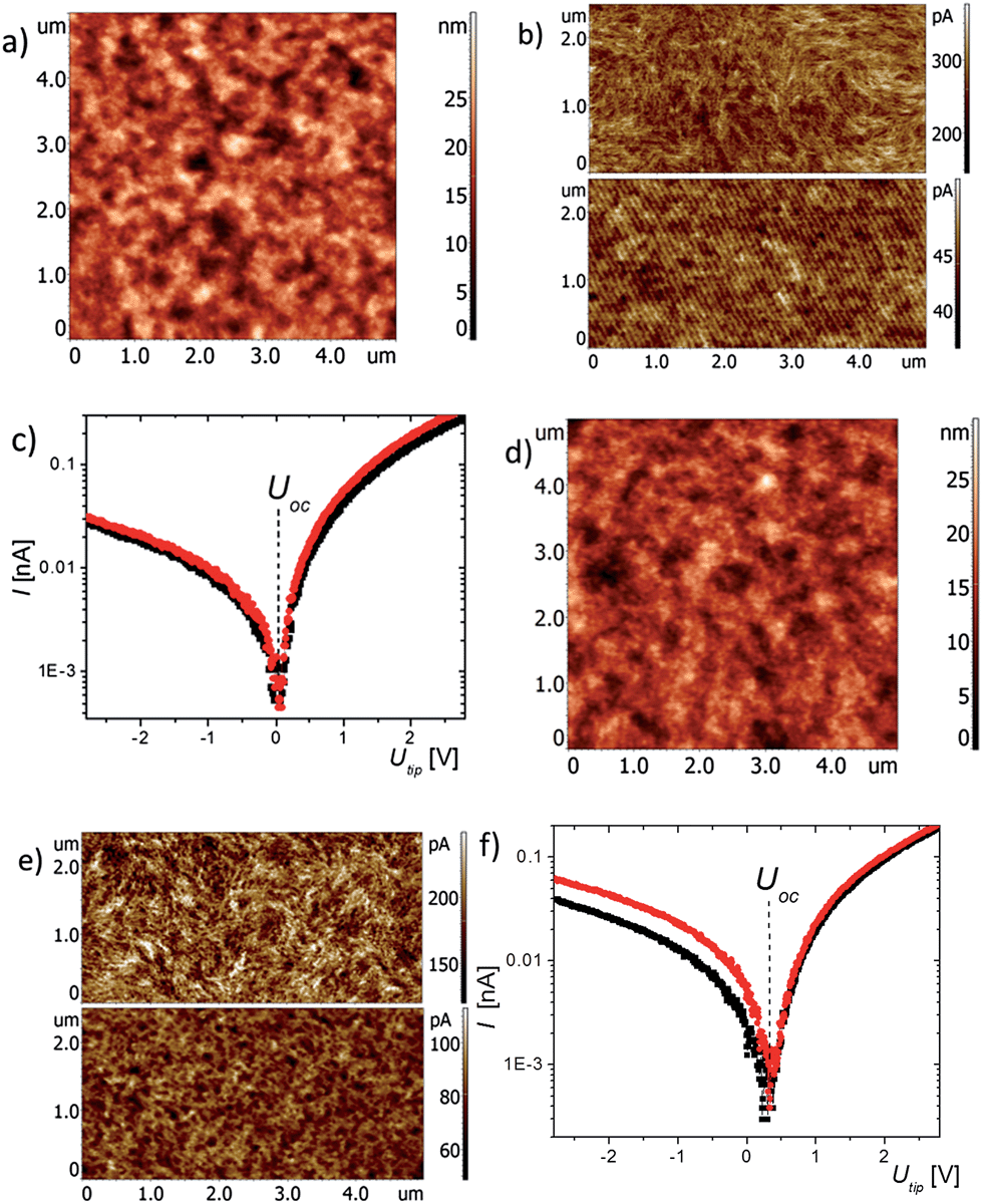
We now turn our attention to the influence of some of the revealed morphology features on the local electrical properties of the blend. AFMs equipped with conductive probes have been used for measurements of local conductivity and photoconductivity in many recent works.22–25 We have used an AFM placed in a nitrogen filled glovebox for local conductivity measurements on PTB7:PC71BM films deposited onto ITO/PEDOT:PSS. For a more detailed investigation an additional sample of PTB7:PC71BM has been prepared by film deposition on glass/Aluminium. The geometry of our setup allows for direct illumination of the tip-sample area by the AFM red laser and thus measured current is photocurrent, since the laser wavelength (670 nm) is near the maximum of PTB7 light absorption.
Fig. 4a and b demonstrate that with short circuit conditions (Utip = 0 V) no current is detected on the film deposited on PEDOT:PSS and there is clear contrast in current image obtained on the film deposited on aluminium. This behaviour is also illustrated by local current–voltage characteristics shown in Fig. 5c and d. The reason for this could be that work function of Au-coated probe is close to the PEDOT:PSS work function, and as a result a weak electric field across the device at short circuit conditions cannot provide any detectable photocurrent. When aluminium is used as substrate the difference of work functions between electrodes is higher and, due to the higher built-in electric field, C-AFM is capable of measuring photocurrent. In the case of an aluminium electrode the device has an inverted structure. The results in Fig. 4b clearly show that with our set-up the photoconductivity is measured.
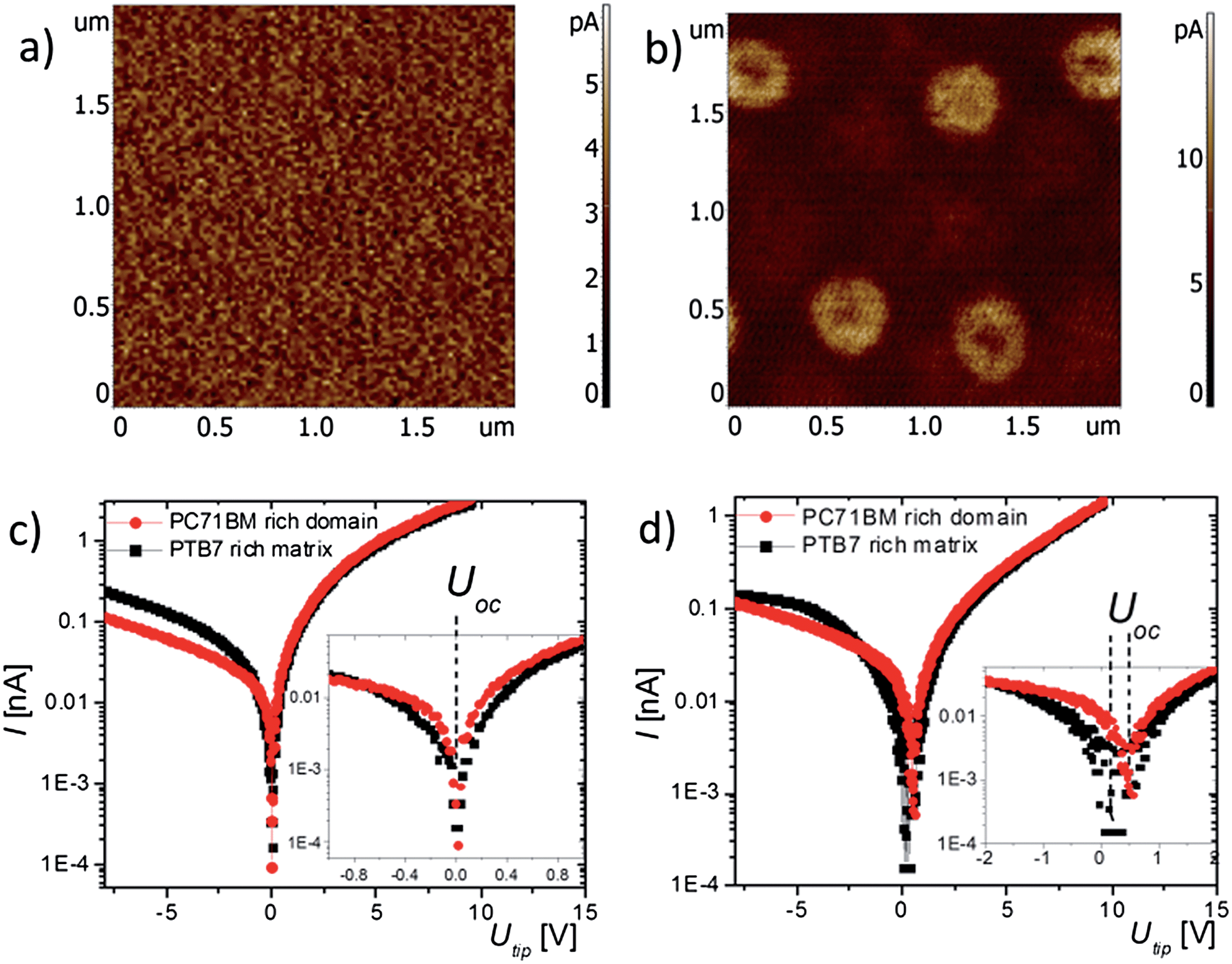 | ||
| Fig. 4 Conductivity distribution at Utip = 0 V and average I–V curves on the surface of PTB7:PC71BM films without DIO deposited on PEDOT:PSS (a & c) and aluminium (b & d). | ||
 | ||
| Fig. 5 Topography (a) and C-AFM images (b–e) obtained at Utip: (b) +0.5 V, (c) +3 V, (d) −0.5 V, (e) −3 V; (f) cross-section of (e). The white arrows indicate same domain. | ||
Topography of a PTB7:PC71BM film deposited on Al differs from that on PEDOT:PSS as the distance between domains is larger (Fig. S3a†). The majority of the domains in the film on PEDOT:PSS are placed with a distance of less than 200 nm in between them, while on Al it is usually in the range 500–1000 nm. In our following discussion we assume that the basic morphological features of both films are same: i.e. they consist of domains embedded into a matrix. However, some details of the substructure in the domains and matrix can be different, which implies that a direct comparison of all local properties may not be always relevant. Since we do not know all details of the morphology of both films, we will do any comparison of local properties only as an assumption. For example, Fig. 4b shows that the photocurrent is detected from the matrix region between domains. This indicates the presence of a bulk heterojunction in the vicinity of the AFM tip when it is placed at the matrix, i.e. there are PC71BM particles inside a PTB7-rich matrix forming a bulk heterojunction. This fact can be used as an additional support for model where PC71BM particles inside a PTB7 matrix exist in film on PEDOT:PSS if we assume a similar structure of matrix of both samples.
The variations of Uoc measured at locations on the domains and matrix of film on Al (Fig. 4d) may be explained by a dependence of the local Uoc on the morphology. At the same time there are no such variations of Uoc in the sample with ITO/PEDOT:PSS (Fig. 4a). This might be a result of different locations of domains inside the polymer-rich matrix. If domains in sample with ITO/PEDOT:PSS are not touching both electrodes then contact only to the polymer exist in the structure PEDOT:PSS/film/Au-tip, leading to a uniform Uoc on sample surface. If the domains in the sample with Al covered by the polymer are in contact with the Al electrode then a different Uoc will be detected at the domains versus at matrix. In this case variations of Uoc are the result of measurements of structures Al/domain/skin layer/Au-tip and Al/PTB7-rich matrix/Au-tip. This example shows that some details of morphologies are different in two samples.
The dependence of the local conductivity images on the voltage applied to the probe for a sample with PEDOT:PSS is shown in Fig. 5. The contrast in Fig. 5 reflects differences between I–V curves in Fig. 4c. At Utip = +0.5 V and −0.5 V the current inside PC71BM rich domains appears in the shape of either rings or circles (Fig. 5b and d) and at both polarities the current distribution is very similar, despite the direction of charge movement being opposite. Localization of photocurrent at PC71BM rich domains can be explained by the influence of a bulk heterojunction formed by the PTB7-rich skin layer and the PC71BM-rich domain, which is placed close to the film surface and thus improves charge transport. The reduced current level in the centre of the ring-shaped current domains could be related to the PTB7-rich skin layer thickness variations, which leads to reduced photocurrent on very top of some of domains where the skin layer is very thin. This also agrees with the fact that light is absorbed mainly by PTB7 when the sample is illuminated by 670 nm tip light. At large positive voltages (Fig. 5c) holes are injected from the tip and the measured current is the result of combination of photocurrent and injected current. This is confirmed by the presence of the same areas with reduced current as in Fig. 5b and d in the central parts of some of the domains at Utip = +3 V. Corresponding to the energy levels of PC71BM and PTB7,6 the injected current in PEDOT:PSS/PTB7:PC71BM/Au structure should be mainly hole current through PEDOT:PSS/PTB7/Au (for energy levels see Fig. S4†). At large negative voltage (Utip = −3 V) holes are injected from PEDOT:PSS and the current distribution image is similar to the expected resistivity of film when holes are flowing through PTB7, i.e. lower resistance is between PC71BM rich domains (Fig. 5e). A cross-section of Fig. 5e shows a different value of current collected at different domains (Fig. 5f). This difference can be explained by the different thicknesses of the skin layer, which influences resistance. The contrast in the current distribution images (Fig. 5) is formed by the difference between I–V characteristics at different points on the surface. At low voltages the difference between currents in the domains and the matrix is determined mainly by photocurrent, while at higher voltages injected current dominates (inset in Fig. 4c). At higher positive voltages the curves are nearly overlapping, which implies weak contrast between the domains and the matrix when holes are injected from the tip (Fig. 5c). Disappearance of the current circles at increased voltages is due to current injection by the tip at high bias. It is also observed in Fig. 4c that the contrast between the domain and matrix changes sign when negative Utip is in the range ∼−0.6 to −0.8 V. This can be interpreted as transition from a low voltage range, where photocurrent dominates, to a region where the injected current determines contrast at negative biases.
In contrast to the I–V curves on a PEDOT-deposited film, the I–V curves obtained on a film deposited onto aluminium are shifted with respect to 0 (Fig. 4d). As can be seen from Fig. 4d, the contrast in the current image disappears at Utip ∼ 0.4 V, which is a local open circuit voltage on the domains. The macroscopic open circuit voltage for solar cells based on pristine blend is Uoc ∼ 0.7 V.12 The difference between local and macroscopic Uoc can be explained by different electrode configurations (Al–Au in C-AFM measurements vs. PEDOT:PSS-Ca in a functional solar cell), different illumination parameters, different electric field configuration near the sharp tip and between flat electrodes or the possible presence of dipoles near electrodes in complete devices. From electrical property mapping it can be concluded that in PTB7:PC71BM blends without additive, only areas near the domains contribute significantly to the photovoltaic effect, while the matrix has a very small influence on macroscopic short circuit current measured for the complete device.
There is no direct evidence of the influence of the granular structure in the film on the current, however, the existence of PC71BM in the PTB7-rich matrix (and, consequently, a bulk heterojunction) is confirmed for the sample on Al by a non-zero open circuit voltage measured in the matrix (Fig. 4d), which is a consequence of a bulk heterojunction between both components localized in the vicinity of the AFM tip. Also the current distribution inside the matrix in Fig. 4b, S3d and S3e† is not uniform, which may be related to PC71BM particles in the polymer matrix.
We now turn out attention to the PTB7:PC71BM blend with 3% of the additive DIO added to the solution prior to spin coating, which enables the highest OPV efficiencies to be obtained. We have previously reported12 initial PC-AFM measurements on this blend with 3% DIO, while here we have been able to look in more detail, applying EFTEM, AFM and PC-AFM with bias and electrode variation to provide greater evidence for the optimum morphology in this high performance photovoltaic blend. Firstly, we can observe results obtained by EFTEM and AFM phase imaging (Fig. 6). There is a significantly decreased size of features visible in all data in Fig. 6 when compared to the case without DIO in Fig. 1.
 | ||
| Fig. 6 PTB7:PC71BM with 3% DIO (Sample 2). (a) EFTEM sulfur map. AFM topography (b) and phase image (c) in hard tapping. | ||
Previously we have observed12 a fibre-like morphology, and this can be partially observed as a non-uniformity in the EFTEM image when looking at the sulfur map (Fig. 6a), where it is clear that there is some connectivity, or structure, observed. The small size of the domains and the high degree of mixing between PTB7 and PC71BM leads to a very weak TEM contrast and overlapping of features when looking through film which explains the lack of very obvious fibre morphology. In particular PTB7 rich fibres in the EFTEM image are not so pronounced because we see a projection of the bulk. In addition, unfortunately no variation in the carbon map in the blend with DIO was observed due to the well-mixed nature of the two materials. Lateral organization of this blend has been previously investigated, and it was found12 with SEM and AFM that the skin layer that is observed without DIO is no longer present in the films with 3% DIO, indicating that good mixing is present between the polymer and fullerene. Turning to the AFM data on the sample (Fig. 6b and c) AFM topography and phase images, measured in hard tapping (domination of repulsive tip-sample forces), also confirm the small domain size of Sample 2. No obvious fibre-like structure is observed in conventional AFM due to the high degree of mixing between the two materials, and thus there are only very subtle mechanical differences (e.g. hardness) between PTB7-rich and PC71BM-rich regions of the blend. These differences are so small that they cannot be measured conventionally.
We have, however, found success in using photoconductive-AFM to enable discrimination between the two material-rich domains. For PC-AFM analysis again two samples with DIO were prepared: one deposited on glass/ITO/PEDOT:PSS and second one deposited on glass/aluminium, and are shown in Fig. 7. Both the topography and contrast of the current distribution images are very similar for aluminium- and PEDOT-deposited samples. This tells us that the nanoscale morphology produced when spin-coating onto quite different substrates is very similar, indicating the resilience of the materials to self-organize whether being deposited onto a polymer or metal. The electrical structure of Sample 2 differs from the structure measured by TEM and AFM. The fibres are clearly seen in current image at positive bias, when holes are injected from tip, while a completely different structure has been detected at negative Utip, showing small particles. The fibre structure of sample deposited on PEDOT has been observed at different voltages from Utip = +0.5 V up to +6 V; at Utip = 0 no current was detected with our setup. The completely different contrast at negative Utip can be explained by different conditions for hole injection, i.e. the PEDOT:PSS and aluminium contacts may be responsible for it. This hypothesis is in agreement with observation of similar pattern at negative Utip in another OPV material deposited on PEDOT:PSS.26 Two different I–V curves measured at places with low and high current demonstrate an evolution of contrast with voltage applied in the sample deposited on PEDOT:PSS (Fig. 7c).
 | ||
| Fig. 7 AFM results for the blend with DIO deposited on PEDOT:PSS (a–c) and deposited on aluminium (d–f). Topography is shown in (a & b), while current distributions are shown in (b & e), with Utip = +3 V (top) and −3 V (bottom); (c and f) typical I–V curves on domains (black line) and off domains (red line). | ||
Local open circuit voltages measured at different places are close to 0 for this sample. I–V curves measured at different points on the PTB7:PC71BM:DIO film deposited on aluminium have local Uoc = +0.3 to +0.4 V (Fig. 7f), which is close to the local Uoc of a pristine sample measured on a PC71BM rich domain. The macroscopic Uoc for the complete device made with DIO additive and a calcium top electrode is ∼0.7 V, therefore the difference between the local and macroscopic Uoc is similar to that of a pristine blend, and can be explained as being due to the same mechanisms. Good intermixing of PTB7 and PC71BM in films with DIO leads to a larger total surface area between the materials with a high photovoltaic effect measured on the surface of the photoactive layer than that of the pristine blend. This leads to a larger macroscopic short circuit current in complete devices and, finally, larger PCE in devices produced with DIO. Another possible reason for higher PCE in such devices can be larger total area of PC71BM domains on film surface in comparison with devices without DIO, which improves charge transport due to better contact between fullerene and electrode. However, based on the morphology observed so far this is only a tentative suggestion.
Experimental
Sample preparation
ITO-coated glass substrates (15 Ω per square) from Xin Yan Technology Ltd were used. The substrates cleaned by sonication in deionized water, acetone and isopropanol and then dried prior to layer depositions. Poly(3,4-ethylenedioxythiophene): poly(styrenesulfonate) (PEDOT:PSS) (Clevios AI4083) was spin-coated at 4000 rpm onto the ITO. The PEDOT:PSS-coated ITO substrates were annealed on a hotplate at 120 °C for 20 min before being placed in a nitrogen-filled glovebox. PTB7:PC71BM solutions were prepared with a total concentration of 25 mg ml−1 at a 1![[thin space (1/6-em)]](https://www.rsc.org/images/entities/char_2009.gif) :1.5 weight ratio in chlorobenzene. The solution was left to dissolve in a glovebox for 5 hours with gentle stirring and 50 °C heating prior to spin coating. The blend was deposited in the glovebox with a spin speed of 1000 rpm for 60 seconds. For solutions that contained 3% by volume of DIO the samples were placed under 10−5 mbar vacuum after deposition to remove any residual DIO.
:1.5 weight ratio in chlorobenzene. The solution was left to dissolve in a glovebox for 5 hours with gentle stirring and 50 °C heating prior to spin coating. The blend was deposited in the glovebox with a spin speed of 1000 rpm for 60 seconds. For solutions that contained 3% by volume of DIO the samples were placed under 10−5 mbar vacuum after deposition to remove any residual DIO.
For plan view TEM measurements the samples were immersed into water and then photoactive layer floating on water surface was picked up by TEM grid.
Measurements
TEM measurements and tomography were performed with TEM Tecnai T20 (FEI) equipped with LaB6 filament and operated at 200 kV with a Gatan Image Filter GIF2000.The commercial AFMs Solver Next (NT-MDT) and SmartSPM (AIST-NT) were utilized for measurements. Conductivity measurements with AFM were performed by Solver P47H (NT-MDT) in nitrogen-filled glove-box (MBraun). The noncontact probes NSG11, NSG20 (NT-MDT) and conductive probes NSC36/Cr–Au and DCP18/Pt (Micromash) were used in AFM measurements.
Current–voltage characteristics are averaged from 3 independent measurements. Tip-sample force in C-AFM measurements was about 20 nN. Au coated probes were used for all C-AFM measurements. The samples were grounded and voltage was applied to the probe. The tip-sample force in C-AFM was adjusted in such a way that there are no visible changes in topography measured in tapping mode after C-AFM regime. The KPM measurements were performed with a Pt-coated probe by using a standard two-pass technique. The topography was measured during the first pass and surface potential was measured during the second pass. For surface potential measurements the amplitude of cantilever oscillations, induced by AC voltage, was nullified by applying the DC voltage between tip and sample. A plasma etching device (Fischione) with argon/oxygen plasma was utilized for sample etching.
Lamella preparation
In-depth measurements were performed on the thin (thinner than 100 nm) lamella with sample cross-section, which has been cut by Focused Ion Beam (FIB) using Ga ions for surface modification (the dual beam system Nova Nanolab (FEI)). For this purpose before ion milling the surface of sample was covered by an electron and ion beam deposited platinum layer, and after FIB cutting the obtained lamella with device cross-section was attached to the Omniprobe TEM grid. The standard procedure for lamella preparation written as a script provided by FEI Co. was implemented for lamella preparation. The initial ion milling of thick lamella was performed with 30 kV accelerating voltage and 15 nA ion current and then these parameters were gradually decreased down to 2 kV and 28 pA for final lamella thinning in order to minimize sample structure modification.27EFTEM analysis
Elemental maps were obtained by EFTEM using the three-window elemental mapping method.15–18 For carbon mapping three energy-loss images were acquired in the vicinity of the carbon K-edge: two pre-edges at 252 and 272 eV, and a post-edge at 294 eV. For sulfur mapping the sulfur L-edge was used: 130 eV first pre-edge, 150 eV for second pre-edge and 185 eV for the post-edge. A filter slit width of 10–20 eV was used (20 eV width was used for cross-section measurements and tomography), the collection angle was 12 mrad, the typical frame time was in the range 3–30 s. Brighter areas in EFTEM images correspond to higher content of corresponding element.EFTEM tomography
Polystyrene latex spheres of ∼50 nm in diameter were used as fiducial markers for TEM tomography reconstruction. A single-axis tilt series was acquired with Technai T20 over an angular range of ±62°, with increment of 2° between consecutive projections (a total of 63 projections), in a manual regime. Carbon maps were obtained at each tilt using the three-window elemental mapping method.15 The outputs of the 1024 × 1024 pixel detector in the GIF2000 were both binned to 512 × 512 pixels to improve the signal to noise ratio. Images and spectra were acquired and processed by means of Gatan Microscopy Suite (Gatan Inc). When specimen drift occurred between acquisition of the pre-edge and post-edge images, it was corrected by automated alignment using cross-correlation. An elemental map tilt series were generated from the three aligned images at each tilt. After obtaining the elemental map tilt series, an automated spatial drift correction (alignment) for the EFTEM series was performed with the Statistically Determined Spatial Drift algorithm using the SDSD plug-in for Digital Micrograph (DM).28 Three-dimensional reconstruction was performed using the simultaneous iterative reconstructive technique (SIRT) as implemented in IMOD tomography reconstruction software with 20 iterations.29 The visualization of all the reconstructions was done using the Amira 5.4.3 software package from FEI Visualization Sciences Group.HAADF-STEM imaging
TEM JEOL ARM200F was employed for HAADF-STEM regime with accelerating voltage of 200 kV, camera length 60 mm, probe current 12 nA and probe size 3 nm. The collection angles were 67–250 mrad. Electron dose for conditions of Fig. 3 (1024 × 1024 points) was <7 × 10⁵ electrons per nm2. This value is smaller than dose used for imaging of different electron beam sensitive polymer materials,20 which ensure small sample damage.Conclusions
The volume structure and local conductivity of PTB7:PC71BM spin-coated films with and without DIO has been investigated using TEM and AFM methods. It was found that PC71BM-rich domains in a film deposited from chlorobenzene solution without additive have nearly ellipsoidal shape. As revealed by both TEM and AFM, the volume of the pristine PTB7:PC71BM blend is not uniform and consists of particles with diameters of several tens nanometres. PC71BM rich domains are embedded into a PTB7 rich matrix and the thickness of the skin layer on both sides of film significantly varies from one domain to another one. The local I–V curves and evolution of current distribution contrast with tip bias were measured for both pristine PTB7:PC71BM films and films spin-coated with the addition of DIO. The features of the local electrical structure of both films have been revealed and connected with the measured morphology. In terms of local electrical properties, the higher power conversion efficiency for the device with DIO can be explained by a larger area of the sample with a noticeable photovoltaic effect, in contrast to the sample without DIO, where only areas near the domains contribute significantly to short circuit current.Acknowledgements
This work was supported by EPSRC (EP/I013288/1). I.D.W.S. was partly supported by the European Union Seventh Framework Programme under grant agreement 321305 and a Royal Society Wolfson Research Merit Award. Part of the work of A.A. and O.A was supported by Ministry of Education and Science of Russian Federation, project 14.A18.21.0887 and the Russian Government Program of Competitive Growth of Kazan Federal University. The authors would like to thank Jeol Japan, Dr David Miller and Prof. John Irvine (University of St Andrews) for measurements with TEM ARM200F. Authors are grateful to Prof. G. de With (Eindhoven University of Technology, The Netherlands) for opportunity to use the integrated AFM-glovebox setup and to Dr A. Kodentsov and Dr D. MacLaren for their help with TEM results interpretation.Notes and references
- C. J. Brabec, N. S. Sariciftci and J. C. Hummelen, Adv. Funct. Mater., 2001, 11, 15 CrossRef CAS.
- X. Yang, J. Loos, S. C. Veenstra, W. J. H. Verhees, M. M. Wienk, J. M. Kroon, M. A. J. Michels and R. A. J. Janssen, Nano Lett., 2005, 5, 579 CrossRef CAS PubMed.
- S. D. Oosterhout, M. M. Wienk, S. S. van Bavel, R. Thiedmann, L. J. A. Koster, J. Gilot, J. Loos, V. Schmidt and R. A. J. Janssen, Nat. Mater., 2009, 8, 818 CrossRef CAS PubMed.
- G. Yu, J. Gao, J. C. Hummelen, F. Wudl and A. J. Heeger, Science, 1995, 270, 1789 CAS.
- S. E. Shaheen, C. J. Brabec, N. S. Sariciftci, F. Padinger, T. Fromherz and J. C. Hummelen, Appl. Phys. Lett., 2001, 78, 841 CrossRef CAS PubMed.
- Y. Liang, Z. Xu, J. Xia, S.-T. Tsai, Y. Wu, G. Li, C. Ray and L. Yu, Adv. Mater., 2010, 22, E135 CrossRef CAS PubMed.
- Z. He, C. Zhong, S. Su, M. Xu, H. Wu and Y. Cao, Nat. Photonics, 2012, 6, 591 Search PubMed.
- S. J. Lou, J. M. Szarko, T. Xu, L. Yu, T. J. Marks and L. X. Chen, J. Am. Chem. Soc., 2011, 133, 20661 CrossRef CAS PubMed.
- M. R. Hammond, R. J. Kline, A. A. Herzing, L. J. Richter, D. S. Germack, H.-W. Ro, C. L. Soles, D. A. Fischer, T. Xu, L. Yu, M. F. Toney and D. M. DeLongchamp, ACS Nano, 2011, 5, 8248 CrossRef CAS PubMed.
- B. A. Collins, Z. Li, J. R. Tumbleston, E. Gann, C. R. McNeill and H. Ade, Adv. Energy Mater., 2012, 3, 65 CrossRef.
- F. Liu, W. Zhao, J. R. Tumbleston, C. Wang, Y. Gu, D. Wang, A. L. Briseno, H. Ade and T. P. Russell, Adv. Energy Mater., 2014, 4, 1676 Search PubMed.
- G. J. Hedley, A. J. Ward, A. Alekseev, C. T. Howells, E. R. Martins, L. A. Serrano, G. Cooke, A. Ruseckas and I. D. W. Samuel, Nat. Commun., 2013, 4, 2867 Search PubMed.
- R. Magerle, Phys. Rev. Lett., 2000, 85, 2749 CrossRef CAS.
- H. Bodiguel, H. Montes and C. Fretigny, Rev. Sci. Instrum., 2004, 75, 2529 CrossRef CAS PubMed.
- R. F. Egerton, Electron energy-loss spectroscopy in the electron microscope, Springer, New York, USA, 2011, p. 491 Search PubMed.
- M. Weyland and P. A. Midgley, Microsc. Microanal., 2003, 9, 542 CrossRef CAS PubMed.
- A. Berger and H. Kohl, Microsc., Microanal., Microstruct., 1992, 3, 159 CrossRef.
- G. Kothleitner and F. Hofer, Micron, 1998, 29, 349 CrossRef CAS.
- S. J. Pennycook, Ultramicroscopy, 1989, 30, 58 CrossRef.
- J. Loos, E. Sourty, K. Lu, G. de With and S. van Bavel, Macromolecules, 2009, 42, 7 CrossRef.
- E. Sourty, S. van Bavel, K. Lu, R. Guerra, G. Bar and J. Loos, Microsc. Microanal., 2009, 15, 251 CrossRef CAS PubMed.
- D. C. Coffey, O. G. Reid, D. B. Rodovsky, G. P. Bartholomew and D. S. Ginger, Nano Lett., 2007, 7, 738 CrossRef CAS PubMed.
- L. S. C. Pingree, O. G. Reid and D. S. Ginger, Nano Lett., 2009, 9, 2946 CrossRef CAS PubMed.
- X.-D. Dang, A. Mikhailovsky and T.-Q. Nguyen, Appl. Phys. Lett., 2010, 97, 113303 CrossRef PubMed.
- X.-D. Dang, A. B. Tamayo, J. Seo, C. V. Hoven, B. Walker and T.-Q. Nguyen, Adv. Funct. Mater., 2010, 20, 3314 CrossRef CAS.
- A. Alexeev, J. Loos and M. M. Koetse, Ultramicroscopy, 2006, 106, 191 CrossRef CAS PubMed.
- M. Schaffer, B. Schaffer and Q. Ramasse, Ultramicroscopy, 2012, 114, 62 CrossRef CAS PubMed.
- B. Schaffer, W. Grogger and G. Kothleitner, Ultramicroscopy, 2004, 102, 27 CrossRef CAS PubMed.
- J. R. Kremer, D. N. Mastronarde and J. McIntosh, J. Struct. Biol., 1996, 116, 71 CrossRef CAS PubMed.
Footnote |
| † Electronic supplementary information (ESI) available. See DOI: 10.1039/c5ta01224d |
| This journal is © The Royal Society of Chemistry 2015 |