
 Open Access Article
 This Open Access Article is licensed under a Creative Commons Attribution-Non Commercial 3.0 Unported Licence
Vertical and lateral morphology effects on solar cell performance for a thiophene–quinoxaline copolymer:PC70BM blend†
Rickard
Hansson
a,
Leif K. E.
Ericsson
a,
Natalie P.
Holmes
b,
Jakub
Rysz
c,
Andreas
Opitz
d,
Mariano
Campoy-Quiles
e,
Ergang
Wang
f,
Matthew G.
Barr
b,
A. L. David
Kilcoyne
g,
Xiaojing
Zhou
b,
Paul
Dastoor
b and
Ellen
Moons
*a
aDepartment of Engineering and Physics, Karlstad University, 65188 Karlstad, Sweden. E-mail: ellen.moons@kau.se
bCentre for Organic Electronics, University of Newcastle, Callaghan, NSW 2308, Australia
cInstitute of Physics, Jagiellonian University, 30-059 Kraków, Poland
dDepartment of Physics, Humboldt-Universität zu Berlin, 12489 Berlin, Germany
eInstitut de Ciència de Materials de Barcelona (ICMAB-CSIC), Campus UAB, Bellaterra, 08193, Spain
fDepartment of Chemistry and Chemical Engineering, Chalmers University of Technology, 41296 Göteborg, Sweden
gAdvanced Light Source, Lawrence Berkeley National Laboratory, Berkeley, CA 94720, USA
First published on 13th February 2015
Abstract
The distribution of electron donor and acceptor in the active layer is known to strongly influence the electrical performance of polymer solar cells for most of the high performance polymer:fullerene systems. The formulation of the solution from which the active layer is spincoated plays an important role in the quest for morphology control. We have studied how the choice of solvent and the use of small amounts of a low vapour pressure additive in the coating solution influence the film morphology and the solar cell performance for blends of poly[2,3-bis-(3-octyloxyphenyl)quinoxaline-5,8-diyl-alt-thiophene-2,5-diyl] (TQ1) and [6,6]-phenyl C71-butyric acid methyl ester (PC70BM). We have investigated the lateral morphology using atomic force microscopy (AFM) and scanning transmission X-ray microscopy (STXM), the vertical morphology using dynamic secondary ion mass spectrometry (d-SIMS) and variable-angle spectroscopic ellipsometry (VASE), and the surface composition using near-edge X-ray absorption fine structure (NEXAFS). The lateral phase-separated domains observed in films spincoated from single solvents, increase in size with increasing solvent vapour pressure and decreasing PC70BM solubility, but are not observed when 1-chloronaphthalene (CN) is added. A strongly TQ1-enriched surface layer is formed in all TQ1:PC70BM blend films and rationalized by surface energy differences. The photocurrent and power conversion efficiency strongly increased upon the addition of CN, while the leakage current decreased by one to two orders of magnitude. The higher photocurrent correlates with the finer lateral structure and stronger TQ1-enrichment at the interface with the electron-collecting electrode. This indicates that the charge transport and collection are not hindered by this polymer-enriched surface layer. Neither the open-circuit voltage nor the series resistance of the devices are sensitive to the differences in morphology.
1. Introduction
The active layer of a polymer solar cell typically consists of a blend of an electron-donating conjugated polymer and an electron-accepting fullerene derivative. For many systems the impact of the morphology of the active layer on the solar cell performance has been demonstrated.1–5 Polymer blend systems that display laterally phase separated domains have been studied extensively by a variety of microscopy techniques.6–17 A common way of varying and controlling the morphology of a donor/acceptor system is through the choice of processing solvents and the use of solvent additives during film formation.1,6,14–18 This change in morphology is often accompanied by improved performance. As reviewed by Liao et al.,16 the effect of additives on the film morphology and device performance depends strongly on the material system in use.Besides lateral structure, vertical phase separation has been observed for several systems. Surface enrichment of polymer at the free surface in polymer:fullerene blend films has previously been observed by dynamic secondary ion mass spectrometry (d-SIMS),19–21 near-edge X-ray absorption fine structure (NEXAFS) spectroscopy,21–23 ultraviolet photoelectron spectroscopy,24 X-ray photoelectron spectroscopy,25 ellipsometry26,27 and high kinetic energy X-ray photoelectron spectroscopy.28 These studies were mainly focused on poly[(9,9-dioctylfluorenyl-2,7-diyl)-co-5,5-(4′,7′-di-2-thienyl-2′,1′,3′-benzothiadiazole)] (APFO-3) and poly(3-hexylthiophene) (P3HT) respectively, blended with [6,6]-phenyl-C61-butyric acid methyl ester (PC60BM).
Poly[2,3-bis-(3-octyloxyphenyl)quinoxaline-5,8-diyl-alt-thiophene-2,5-diyl] (TQ1) is an easily synthesized polymer29 that, mixed with the fullerene derivative [6,6]-phenyl C71-butyric acid methyl ester (PC70BM), has demonstrated a solar cell power conversion efficiency (PCE) of 7%.30 For TQ1:PC70BM solar cells, spincoated from a single solvent, ortho-dichlorobenzene (oDCB) has so far given the highest PCE.29,30 The addition of small amounts of the high boiling point 1-chloronaphthalene (CN), significantly improved the device performance, assigned by Kim et al. to the smoother lateral morphology of the films.30
Here we study how the use of different solvents affects the lateral and vertical structure of spincoated thin films of TQ1:PC70BM blends. We extend the previously reported studies on lateral morphology by using a set of tools to probe the chemical composition distribution vertically through the film (d-SIMS and variable-angle spectroscopic ellipsometry (VASE)), laterally (atomic force microscopy (AFM) and scanning transmission X-ray microscopy (STXM)) as well as at the surface (NEXAFS). To evaluate the effect of the morphological differences on the device performance, solar cells processed from different solvents with and without additives were prepared and characterized.
2. Experimental section
2.1 Materials
The molecular structure of TQ1 and PC70BM are shown in Fig. 1b. The synthesis of TQ1 is described elsewhere.29 The number average and weight average molecular weights, determined by size exclusion chromatography relative to polystyrene standards, were Mn = 34 kg mol−1 and Mw = 91 kg mol−1 for all samples except for the STXM samples where they were Mn = 70 kg mol−1 and Mw = 265 kg mol−1. The molecular weight differences in this range do not affect the overall trends in morphology. Small variations in film thickness due to the molecular weight differences were compensated by adjusting the solution concentrations. The mass density of TQ1 is estimated to be 1 g cm−3.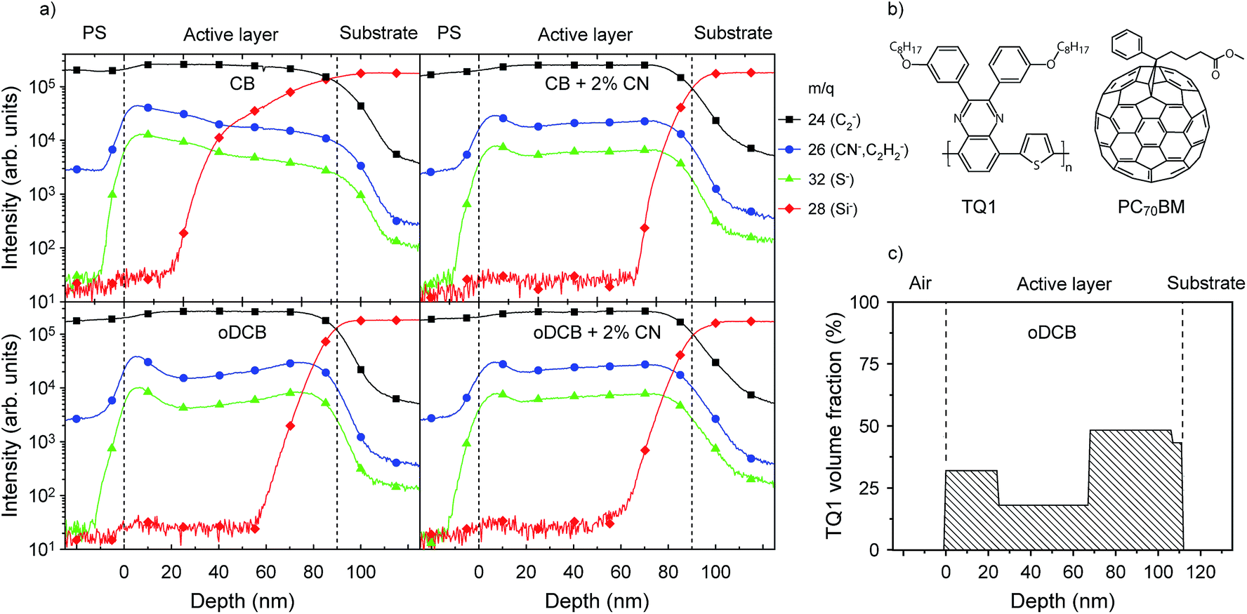 | ||
Fig. 1 (a) d-SIMS depth profiles for TQ1:PC70BM 1![[thin space (1/6-em)]](https://www.rsc.org/images/entities/char_2009.gif) :3 w/w films spincoated on silicon substrates from CB, CB + 2% CN, oDCB and oDCB + 2% CN. PS refers to the polystyrene sacrificial layer. The vertical dashed lines mark the top and bottom of the active layer; the top of the active layer is drawn where the intensity of the S− signal (green) has reached 50% of the maximum intensity value of the first peak whereas the bottom of the active layer is drawn where the C2− signal has dropped to 50% of its saturation intensity inside the active layer. For more details on the interpretation of the m/q = 26 signal, see the ESI.† (b) Molecular structures of TQ1 and PC70BM. (c) Ellipsometrically deduced polymer volumetric depth profile for a TQ1:PC70BM 1:3 w/w film spincoated from oDCB onto silicon. :3 w/w films spincoated on silicon substrates from CB, CB + 2% CN, oDCB and oDCB + 2% CN. PS refers to the polystyrene sacrificial layer. The vertical dashed lines mark the top and bottom of the active layer; the top of the active layer is drawn where the intensity of the S− signal (green) has reached 50% of the maximum intensity value of the first peak whereas the bottom of the active layer is drawn where the C2− signal has dropped to 50% of its saturation intensity inside the active layer. For more details on the interpretation of the m/q = 26 signal, see the ESI.† (b) Molecular structures of TQ1 and PC70BM. (c) Ellipsometrically deduced polymer volumetric depth profile for a TQ1:PC70BM 1:3 w/w film spincoated from oDCB onto silicon. | ||
PC70BM (purity > 99%) was purchased from Solenne BV (The Netherlands). For PC60BM, reported density values31–33 range from 1.3–1.6 g cm−3, and the mass density of PC70BM has been reported to be the same as for PC60BM.33 Here the value of 1.5 g cm−3 is used for the PC70BM mass density.
Poly(3,4-ethylenedioxythiophene) polystyrene sulfonate (PEDOT:PSS) (Clevios P VP AI 4083) was purchased from Heraeus Precious Metals GmbH & Co. KG.
Chloroform and chlorobenzene (both analytical grade) were purchased from Merck KGaA, ortho-dichlorobenzene (analytical grade) and 1-chloronapthalene (technical grade) were purchased from Sigma-Aldrich Corporation. All chemicals were used as received.
For the morphological characterizations, substrates were cut from silicon wafers (n-type, (001) orientation and resistivity 0.001–0.003 Ω cm) and cleaned using the standard RCA-method,34–36 without the final HF-etching step in order to leave the surface hydrophilic.
For solar cells, patterned ITO-coated glass substrates from Kintec Company, China, with a 200 nm thick ITO layer with sheet resistivity 10 Ω sq−1 were used, which were cleaned in isopropanol in an ultrasonic bath for 60 min and subsequently UV-ozone treated for 20 minutes.
2.2 Sample preparation
The d-SIMS and ellipsometry samples were prepared on Si without additional PEDOT:PSS interlayers in order to facilitate the identification of the interface between the active layer and the substrate. On all other substrates, a 50 nm PEDOT:PSS layer was spincoated after filtering through a 0.45 nm nylon filter. For AFM, NEXAFS and solar cell devices the PEDOT:PSS covered substrates were annealed at 120 °C for 20 minutes in a vacuum oven (∼10−1 mbar).Blend solutions of TQ1:PC70BM in a 1:3 weight/weight ratio were prepared in chlorobenzene (CB), and ortho-dichlorobenzene (oDCB) respectively, with and without the addition of 2% (vol) 1-chloronaphthalene (CN) and in chloroform (CF). The active layer was deposited by spincoating in a protected N2 atmosphere (<0.1 ppm O2, <0.1 ppm H2O) inside a glove box (M. Braun Inertgas-Systeme GmbH). Solution concentrations and spin speeds were chosen with the intention of achieving similar film thicknesses in all samples.
The film thicknesses of the active layers were measured by scanning across a scratch in the film with the tip of an AFM (Nanoscope IIIa Multimode, Veeco Metrology group) in tapping mode using a Si tip. The blend film thicknesses were 90 ± 10 nm, except for the film for ellipsometry that was 110 nm and the film from CF that was 140 ± 20 nm. Achieving a uniform thickness in films from CF was not possible due to the formation of striations.
For the SIMS depth profiling, a 50–100 nm thick sacrificial layer of polystyrene (PS) was deposited on top of the TQ1:PC70BM films by lifting off the PS film from an auxiliary glass substrate onto a water surface and floating it onto the active layer surface. This enables stable sputtering conditions before the TQ1:PC70BM layer is reached and a more accurate analysis of the topmost surface region.
The films for STXM were lifted off their PEDOT:PSS coated Si substrates and floated onto a copper TEM grid (300 mesh).
For the solar cells, after spincoating the active layer, the samples were transferred to the vacuum chamber of the thermal evaporator (Univex 350 G, Oerlikon Leybold Vacuum GmbH) integrated within the glove box before 0.3 nm LiF and 100 nm Al was deposited with a deposition rate of 0.5 Å s−1 (LiF) and 1 Å s−1 (Al) at 10−6 mbar.
2.3 Characterization
The d-SIMS depth profiles (5 nm depth resolution) were obtained using a TOF-SIMS 5 system (ION-TOF GmbH, Münster, Germany) equipped with a 30 keV liquid metal ion gun and a Time-of-Flight mass spectrometer. A 0.5 keV beam of Cs+ ions was used to remove material by sputtering a 300 μm × 300 μm region while a 30 keV pulsed beam of Bi3+ ions was used to analyze the composition of the central 100 μm × 100 μm area in that region. Secondary ions with mass to charge ratios of 24, 26, 28 and 32, corresponding to C2−, CN−, Si− and S− respectively, were collected. The C2− ions monitor the total carbon content in the film, the Si− ions show when the substrate is reached, while the S− and CN− ions act as labels for the TQ1 since sulfur and nitrogen are present in TQ1 but not in PC70BM.VASE was carried out with a RC2 instrument from J. A. Woollam Co., Inc. (USA). The incidence angle was scanned from 45 degrees to 75 degrees in steps of 10 degrees, and the photon energy varied from 0.74 eV to 5.06 eV. Modeling of the blend films was performed using the Winelli II software package. The optical properties of the pure materials (taken from literature37) were mixed through the effective medium approximation and the film was mathematically divided into a discrete number of sublayers. The film thickness and volume fraction of each sublayer were fitted.
NEXAFS spectra were recorded at beamline D1011 of the MAX-IV National Laboratory for Synchrotron Radiation in Lund, Sweden. All NEXAFS spectra were collected near the C1s absorption edge in the photon energy range 276–327 eV at 55° incidence angle with respect to the sample surface. Total electron yield (TEY) spectra were obtained by measuring the sample drain current and partial electron yield (PEY) spectra were collected by a multichannel plate detector with a −150 V retarding voltage applied to the entrance grid. TEY and PEY give different sampling depths, with TEY probing down to 5–10 nm (ref. 38 and 39) and PEY 2–3 nm (ref. 40 and 41) below the surface. Reference spectra were recorded both in TEY and PEY mode of a gold coated mica sample (Georg Albert, PVD-Beschichtungen) that had been cleaned in situ by sputtering with argon. All NEXAFS spectra were divided by their corresponding gold spectrum and normalized in the high photon energy region.38,42 The photon energy scale was calibrated by measuring the spectrum of highly ordered pyrolytic graphite (HOPG) and using the position of the exciton resonance at 291.65 eV as an energy reference.43
The surface composition was obtained from the NEXAFS spectra by finding the linear combination of the pure components' spectra that best matched the spectrum of the blend. The coefficients in that linear combination then give the volume ratio of the components.44 This assumes that the pure components do not react in the blend forming new components, that the electron scattering length is similar in both components, and that possible surface degradation is similar in the blend films compared to the films of the pure components. No degradation of the sample due to exposure to the X-ray beam was observed during the NEXAFS measurements. To compensate for a small drift in photon energy (<0.15 eV) that was caused by the monochromator, the spectra of the pure components were each shifted additionally in steps of 5 meV, ±30 steps, with respect to the blend spectrum until the residual was as small as possible. The uncertainties in composition are estimated based on the size of the residuals, calculated as the relative area of the absolute value of the residual curve (see ESI†) to the blend spectrum.
Contact angles were measured on films of pristine TQ1 and PC70BM using an FTA 200 contact angle equipment (First Ten Ångstroms, USA). The surface energy was calculated from the contact angles between the film and deionized water using the relation by Li and Neumann.45,46
The topography of the samples was examined by AFM in tapping mode using a Si tip.
The STXM measurements were performed on beamline 5.3.2.2 at the Advanced Light Source in Berkeley, USA47 in a helium atmosphere at 0.33 atm. The sample was raster scanned with respect to the X-ray beam and the transmitted X-rays were detected by a scintillator and a photomultiplier tube. The photon energies 284.3 eV for PC70BM and 287.3 eV for TQ1 were used for the image scans.
The current–voltage characteristics of the solar cells were measured using a Keithley 2636A Dual-channel SourceMeter, in a sealed cell with N2 atmosphere under AM 1.5 illumination (Sol2A, model 94022A, from Oriel Instruments, USA) through a 2 mm thick poly(methyl methacrylate) (PMMA) sheet. No spectral correction was made for any UV light absorption by the PMMA. When extracting the photovoltaic parameters, the data points were interpolated using a cubic spline. The series resistance was obtained by fitting the higher voltage part of the forward dark curve to the modified Shockley equation:
| eV = nkBT × ln(j/j0 + 1) + jRS | (1) |
3. Results
Fig. 1a shows the d-SIMS depth profiles for TQ1:PC70BM blend films spincoated on Si substrates from CB, CB + 2% CN, oDCB and oDCB + 2% CN. For clarity, the profile is separated by dashed lines into three regions: the polystyrene (PS) sacrificial layer, the active layer and the Si substrate. All blend films show an increased intensity of the m/q = 26 (CN−) and m/q = 32 (S−) signals near the interface with the PS compared to the rest of the active layer. In the film prepared from CB these TQ1 related signals decrease from the maximum intensity at the interface with PS all the way down to the Si substrate, while in the films prepared from oDCB the TQ1 related profiles go through a minimum at around 20 nm depth. The addition of 2% CN, regardless of being added to CB or oDCB, gives very similar depth profiles for m/q = 26 (CN−) and 32 (S−) in the active layer with a maximum signal intensity near the interface with PS, a minimum at around 20 nm, followed by a slightly increasing profile until the Si interface is reached.The depth profile was also determined independently by VASE. Fig. 1c shows the deduced profile in terms of the polymer volume fraction on a TQ1:PC70BM film spincoated from oDCB onto a silicon wafer, confirming the enrichment of polymer next to both interfaces while the fullerene accumulates in the middle of the film. We found that no further fitting improvement could be obtained when including more than four sublayers, which suggests a depth resolution of around 20 nm in this experiment.
NEXAFS spectra at the C1s edge show X-ray absorption resonances corresponding to transitions from the C1s ground state to molecular empty states, and are therefore used as molecular fingerprints. In Fig. 2, C1s NEXAFS spectra recorded in TEY and PEY mode of pristine TQ1 and pristine PC70BM spincoated from CB are shown. As can be seen in the figure, the TQ1 and PC70BM NEXAFS spectra are quite different, making it possible to compare a blend spectrum to those of the pristine components in order to calculate the chemical composition. These pristine spectra are independent of the solvent, films spincoated from oDCB have identical spectra (not shown). The PEY spectra look similar to the spectra recorded in TEY, apart from differences in relative peak intensities. Many of the main resonances of TQ1 overlap, or partly overlap with those of PC70BM, except for the PC70BM C1s → π* resonance at 284.3 eV that is well separated from any TQ1 resonances. The PC70BM NEXAFS spectrum is similar to what has previously been reported.48
 | ||
| Fig. 2 C1s NEXAFS spectra measured in total electron yield (TEY) and partial electron yield (PEY) of pristine PC70BM and pristine TQ1 films. | ||
Fig. 3 shows C1s NEXAFS spectra, both PEY and TEY, of TQ1:PC70BM blend films spincoated from CB, CB + 2% CN, oDCB and oDCB + 2% CN. The PEY blend spectra look similar to those of pristine TQ1, except for a shoulder at 284.3 eV from PC70BM, which is most pronounced in the film prepared from CB. The TEY blend spectra show, instead of a shoulder, a distinct peak at 284.3 eV, again with the highest intensity in the film prepared from CB. Comparing the 284.3 eV peak intensity between the PEY and the TEY spectra, the intensity is larger in TEY than in PEY for all the solvents.
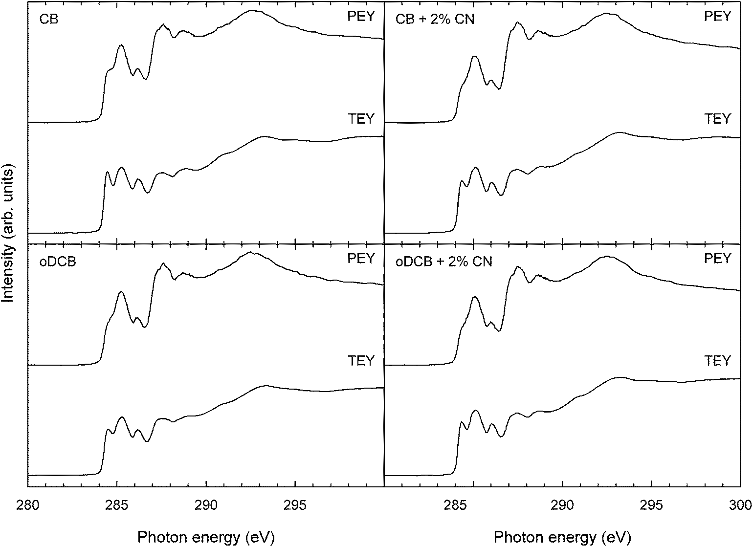 | ||
| Fig. 3 C1s NEXAFS spectra measured in total electron yield (TEY) and partial electron yield (PEY) of TQ1:PC70BM 1:3 w/w blend films spincoated from different solvents with and without 2% of the additive CN. | ||
The mass fractions of TQ1, found by fitting the blend spectra to those of the pristine components, are summarized in Table 1. All the TQ1:PC70BM blends, regardless of solvent, show polymer enriched surfaces with respect to the bulk composition (1:3 w/w). The enrichment is strongest for the blend films made with added CN, and the composition is very similar for CB + 2% CN and oDCB + 2% CN. The PEY spectra, corresponding to regions closer to the surface all show a higher intensity of the C1s → π* resonance at 284.3 eV than the TEY spectra corresponding to the subsurface.
The surface energies of pristine TQ1 and PC70BM were determined from contact angle measurements. The surface energy of TQ1 was found to be 29 mJ m−2 and for PC70BM 39 mJ m−2.
AFM height images, measured in tapping mode, of TQ1:PC70BM blend films spincoated from different solvents are shown in Fig. 4. Domains in the shape of islands are clearly visible in films prepared from CB and oDCB solutions. The size of the domains is strongly dependent on the spincoating solvent, with CB giving typical domains of 200–400 nm diameter and oDCB 50–100 nm diameter. With the addition of 2% CN, both to CB and to oDCB, this lateral domain structure is no longer visible, and the films are smoother compared to when no CN was added. Root mean square (RMS) roughness values are 6.6 nm (CB), 1.3 nm (oDCB), 0.45 nm (CB + 2% CN), 0.47 nm (oDCB + 2% CN). A new fine structure is apparent in the films prepared with additives.
 | ||
| Fig. 4 AFM height images (5 × 5 μm2), of TQ1:PC70BM 1:3 w/w, spincoated from CB, CB + 2% CN, oDCB and oDCB + 2% CN. RMS roughness values are 6.6 nm (CB), 1.3 nm (oDCB), 0.45 nm (CB + 2% CN), 0.47 nm (oDCB + 2% CN). | ||
Fig. 5 shows AFM images along with compositional maps for TQ1 and PC70BM of TQ1:PC70BM blend films spincoated from CF, CB and oDCB. Light colours in the STXM images correspond to high concentrations. The islands observed by AFM correspond to the compositional domains observed in the STXM maps, with similar domain sizes. The STXM maps reveal the bulk morphology, confirming that the protruding islands are PC70BM-rich whereas the surrounding phase is TQ1-rich.
 | ||
| Fig. 5 AFM height (left) and STXM images (middle and right), 2 × 2 μm2, of spincoated TQ1:PC70BM 1:3 w/w films. The height scales of the AFM images are 40 nm for CF and CB and 10 nm for oDCB. The STXM images show composition maps corresponding to mass fractions of PC70BM (middle) and TQ1 (right). Casting solvents are CF (top), CB (middle) and oDCB (bottom). Scale bars are 500 nm. The colour scale of the STXM images is such that light colours correspond to high concentrations. These images show the phase separated domains in the blends whose size decreases from CF to CB to oDCB. | ||
Fig. 6a shows JV-curves under AM 1.5 illumination of TQ1:PC70BM solar cells with active layers spincoated from different solvents, corresponding to the best performing devices. The photovoltaic parameters (mean values ± standard deviations, each from 9 devices) are shown in Table 2. Without any additives, films prepared from oDCB yield more efficient devices than those prepared from CB, which is dominantly due to a higher short circuit current density (JSC) but also because of a slight increase in fill factor (FF). With the addition of 2% CN, devices made from CB and from oDCB both improved in conversion efficiency, due to a large increase in JSC. In the case of the solar cells made from CB, the addition of CN more than doubles the JSC and the PCE reaches 5.5%, without a significant drop in VOC or FF.
 | ||
| Fig. 6 Current–voltage characteristics (a) under illumination and (b) in the dark of the best performing devices made from TQ1:PC70BM, spincoated from different solvents with and without 2% of the additive CN. The series resistance was determined by fitting the high voltage part of the dark curves (full line) to eqn (1). | ||
:3 w/w. Mean values ± standard deviations, each from 9 devices, are shown
| Solvent | J SC (mA cm−2) | V OC (V) | FF (%) | R S (Ω cm2) | PCE (%) |
|---|---|---|---|---|---|
| CB | 4.90 ± 0.14 | 0.90 ± 0.007 | 56.5 ± 2.7 | 3.24 ± 0.59 | 2.50 ± 0.14 |
| CB + CN | 10.46 ± 0.35 | 0.88 ± 0.013 | 59.2 ± 1.7 | 3.04 ± 0.66 | 5.48 ± 0.27 |
| oDCB | 6.54 ± 0.29 | 0.91 ± 0.012 | 62.2 ± 0.8 | 3.26 ± 0.25 | 3.71 ± 0.21 |
| oDCB + CN | 9.29 ± 0.63 | 0.89 ± 0.011 | 59.4 ± 0.8 | 2.78 ± 0.39 | 4.93 ± 0.39 |
Fig. 6b shows the corresponding dark JV-curves of the best performing devices. The series resistance RS is extracted from the high voltage region, while current at the low and reverse bias region is indicative for the leakage current. As can be seen in Table 2, the series resistance of the solar cells is not significantly influenced by the morphology changes. The leakage current in solar cells prepared from solutions containing CN additive is one to two orders of magnitude lower than for the devices prepared without CN.
4. Discussion
The SIMS depth profiles (Fig. 1) show that all the blend films exhibit an increase in TQ1 concentration at the interface between the active layer and the PS, indicating that a TQ1-rich surface layer is formed during spincoating at the free surface in all the blend films. The enrichment of TQ1 at the free surface is consistent with the difference in surface energy between TQ1 (29 mJ m−2) and PC70BM (39 mJ m−2). To minimize the total energy, TQ1, which has the lower surface energy, moves to the surface during the film formation. Polymer-enrichment at the free surface due to surface energy minimization has previously been reported for several other systems.19,21,23,25,49–51The SIMS depth profiles of Si− (m/q = 28) show a steep step for the films prepared from CB + 2% CN, oDCB and oDCB + 2% CN while the Si-profile for the film prepared from CB has an onset at a lower depth value and increases gradually. This early onset is due to a higher surface roughness in the film prepared from CB, as can be seen in the AFM images in Fig. 4. This roughness is carried on into the film as it gets sputtered which translates into broad interfaces in dynamic SIMS profiles. The actual surface composition (TQ1:PC70BM) cannot be reliably deduced from the SIMS depth profile due to variations in detection sensitivities for different elements. The overall depth profile shape is, however, in good agreement with the ellipsometrically deduced profile (Fig. 1c).
Comparing the NEXAFS spectra of the blend films (Fig. 3) with the spectra of the pristine components (Fig. 2), the spectra recorded in PEY mode of the blend films all closely resemble that of pristine TQ1, with the exception of the presence of a shoulder at 284.3 eV, corresponding to the π* resonance of PC70BM. Given the surface sensitivity of the PEY measurement, the absence of a strong peak in the NEXAFS blend spectra despite a 1:3 TQ1:PC70BM blend ratio indicates that far more TQ1 is present at the surface than PC70BM; in agreement with the SIMS results. Moreover, the observation that the PC70BM π* resonance is more pronounced in the CB blend spectra also shows that the degree of polymer enrichment is affected by the casting solvent. In the NEXAFS spectra of the blends recorded in the less surface sensitive TEY mode the PC70BM π* is clearly visible as a separate peak; indicating that the sub-surface, probed by TEY, contains more PC70BM than the surface, probed by PEY. In other words, in the first few nanometers below the surface, a concentration gradient is found for all the blend films, with higher TQ1 enrichment at the topmost surface than in the sub-surface. The quantitative values for the compositions, obtained by fitting the blend spectra as linear combinations of the pristine components' spectra, are shown in Table 1. The deviation between the volume fractions deduced with ellipsometry and NEXAFS is mainly due to the different sensitivities of the two experiments to the surface composition but could also be caused by sample to sample variations (e.g. film thickness).
From the NEXAFS values, we conclude that the samples prepared with solvent additives are more strongly polymer-enriched at the outmost surface than the samples prepared without solvent additives. The different TQ1 surface concentrations could be correlated to the different evaporation rates of the solvents, slowly evaporating solvents allowing the components more time to diffuse. However, effects of the surface roughness cannot be completely excluded. The difference between surface and sub-surface composition for the samples prepared with additives is also larger, indicating a stronger composition gradient.
AFM and STXM images combined show a lateral structure that strongly depends on the casting solvent. The lateral domain structure, observed in AFM and STXM images in the films prepared from CB and oDCB, consists of PC70BM-rich islands surrounded by a TQ1-rich homogenous phase. The decrease in domain size that is observed when CB is replaced by the lower vapour pressure oDCB is perhaps surprising, since the oDCB solution takes a longer time to dry than a CB solution. Films prepared from CF result in even larger domains than those spincoated from CB, despite the very short drying time of such a CF-based film. It is clear therefore that factors other than drying kinetics dominate the phase separation process, such as the difference in PC70BM solubility in these solvents.52–54 The addition of 2% of the additive CN with very high PC70BM solubility55 and very low vapour pressure (Tb = 263 °C) has a drastic effect on the lateral morphology. No lateral phase separation is observed in the films with added CN on the analyzed length scales, similar to what has been reported for other systems.56–58
From the device results it is clear that the performance of the ITO/PEDOT:PSS/TQ1:PC70BM/LiF/Al solar cells strongly depends on solvent. While the VOC, FF and RS remain largely unaffected by the choice of solvent, the dominant effect is on the JSC. Not unexpectedly, there is a strong correlation between the lateral domain size in the active layer and JSC; as the domain size decreases the JSC increases. This observation is in agreement with other reports on TQ1:PC70BM solar cells29,30,59 and several other polymer:fullerene systems6,17,60,61 where increased JSC has been attributed to decreased domain sizes, and rationalized by an improved exciton separation and free charge generation at the donor–acceptor interface.
As can be seen by comparing Tables 1 and 2, the best performing solar cells not only displayed the finest lateral structure, but had also the highest TQ1 enrichment at the free surface. In a simple model of the bulk-heterojunction solar cell operation, one would expect that the charge collection step would benefit from having an enrichment of the electron-accepting material (PC70BM) at the interface with the low work function (Al/LiF) electrode. All TQ1:PC70BM blend films studied here, however, show enrichment of electron-donating material (TQ1) at the free surface upon which the low work function electrode is deposited when constructing a solar cell. Such a TQ1 surface layer might be expected to act as a barrier for electrons, resulting in higher series resistance and poor charge collection. This is, however, not what we observe. Instead, as can be seen in Table 2, the photocurrent is higher for devices with high (up to 85%) TQ1 content at the electron-collecting electrode and the series resistance of the solar cells is not significantly influenced by the morphology differences.
It has also previously been shown for P3HT:PC60BM solar cells, that device performance can be insensitive to surface enrichment of the polymer.22 Even when a thin (8–9 nm) layer of pure P3HT was deposited on top of the P3HT:PC60BM blend film prior to cathode deposition, the devices were not severely impeded. In the case of the TQ1:PC70BM solar cells studied here, the TQ1-rich surface layer below the cathode does not hinder efficient device performance.
5. Conclusions
A TQ1-rich surface layer is formed at the free surface of spincoated thin films of TQ1:PC70BM blends, due to surface energy minimization. The composition of the surface layer depends on the choice of solvent and additives. The solvent additive CN makes the surface enrichment of TQ1 stronger. The addition of CN also resulted in smooth films with fine lateral mixing of donor–acceptor molecules and corresponding high efficiency solar cells due to the increased photocurrent compared to the films with phase separated lateral domain structures prepared without CN additive. The series resistance was unaffected by the morphology. The improved power conversion efficiency of TQ1:PC70BM solar cells upon addition of the solvent additive CN correlates with a finer lateral distribution of donor and acceptor molecules in the film, accompanied by an increased TQ1-enrichment of the surface layer.Acknowledgements
The authors thank Ana Sofia Anselmo and Monika Josiek for valuable experimental contributions in the initial stages of the research project, Christian Müller for the ellipsometry experiment and Alexei Preobrajenski at beamline D1011, MAX-IV Laboratory, for valuable technical advice with the NEXAFS experiments. E.M. acknowledges funding from the Swedish Research Council (Project 2010-4155) and the Göran Gustafsson Foundation for Research in Natural Sciences and Medicine. M.C.-Q. thanks the Spanish Ministerio de Economía y Competitividad for financial support through project PHOTOCOMB (MAT2012-37776). A.O. acknowledges the Röntgen–Ångström–Cluster for financial support. E.W. acknowledges the Swedish Research Council for financial support. This work was performed in part at the Materials node of the Australian National Fabrication Facility, which is a company established under the National Collaborative Research Infrastructure Strategy to provide nano and microfabrication facilities for Australia's researchers. STXM data were acquired at beamline 5.3.2.2 at the Advanced Light Source, Berkeley, which is supported by the Director, Office of Science, Office of Basic Energy Sciences, of the U.S. Department of Energy under Contract no. DE-AC02-05CH11231.References
- J. Peet, A. J. Heeger and G. C. Bazan, Acc. Chem. Res., 2009, 42, 1700–1708 CrossRef CAS PubMed.
- B. Kippelen and J.-L. Brédas, Energy Environ. Sci., 2009, 2, 251–261 CAS.
- A. Salleo, R. J. Kline, D. M. DeLongchamp and M. L. Chabinyc, Adv. Mater., 2010, 22, 3812–3838 CrossRef CAS PubMed.
- M. A. Brady, G. M. Su and M. L. Chabinyc, Soft Matter, 2011, 7, 11065–11077 RSC.
- F. Liu, Y. Gu, J. W. Jung, W. H. Jo and T. P. Russell, J. Polym. Sci., Part B: Polym. Phys., 2012, 50, 1018–1044 CrossRef CAS.
- S. E. Shaheen, C. J. Brabec, N. S. Sariciftci, F. Padinger, T. Fromherz and J. C. Hummelen, Appl. Phys. Lett., 2001, 78, 841–843 CrossRef CAS PubMed.
- J. Liu, S. Yijian and Y. Yang, Adv. Funct. Mater., 2001, 11, 420–424 CrossRef CAS.
- T. Martens, J. D'Haen, T. Munters, Z. Beelen, L. Goris, J. Manca, M. D'Olieslaeger, D. Vanderzande, L. De Schepper and R. Andriessen, Synth. Met., 2003, 138, 243–247 CrossRef CAS.
- H. Hoppe, M. Niggemann, C. Winder, J. Kraut, R. Hiesgen, A. Hinsch, D. Meissner and N. S. Sariciftci, Adv. Funct. Mater., 2004, 14, 1005–1011 CrossRef CAS.
- H. Hoppe, T. Glatzel, M. Niggemann, W. Schwinger, F. Schaeffler, A. Hinsch, M. C. Lux-Steiner and N. S. Sariciftci, Thin Solid Films, 2006, 511–512, 587–592 CrossRef CAS PubMed.
- C. R. McNeill, H. Frohne, J. L. Holdsworth, J. E. Furst, B. V. King and P. C. Dastoor, Nano Lett., 2004, 4, 219–223 CrossRef CAS.
- C. R. McNeill, H. Frohne, J. L. Holdsworth and P. C. Dastoor, Synth. Met., 2004, 147, 101–104 CrossRef CAS PubMed.
- C. R. McNeill, B. Watts, L. Thomsen, W. J. Belcher, A. L. Kilcoyne, N. C. Greenham and P. C. Dastoor, Small, 2006, 2, 1432–1435 CrossRef CAS PubMed.
- F. Zhang, K. G. Jespersen, C. Björström, M. Svensson, M. R. Andersson, V. Sundström, K. Magnusson, E. Moons, A. Yartsev and O. Inganäs, Adv. Funct. Mater., 2006, 16, 667–674 CrossRef CAS.
- Y. Yao, J. Hou, Z. Xu, G. Li and Y. Yang, Adv. Funct. Mater., 2008, 18, 1783–1789 CrossRef CAS.
- H.-C. Liao, C.-C. Ho, C.-Y. Chang, M.-H. Jao, S. B. Darling and W.-F. Su, Mater. Today, 2013, 16, 326–336 CrossRef CAS PubMed.
- M. T. Rispens, A. Meetsma, R. Rittberger, C. J. Brabec, N. S. Sariciftci and J. C. Hummelen, Chem. Commun., 2003, 2116–2118 RSC.
- A. C. Arias, J. Macromol. Sci., Part C: Polym. Rev., 2006, 46, 103–125 CrossRef CAS.
- C. M. Björström, A. Bernasik, J. Rysz, A. Budkowski, S. Nilsson, M. Svensson, M. R. Andersson, K. O. Magnusson and E. Moons, J. Phys.: Condens. Matter, 2005, 17, L529–L534 CrossRef.
- C. M. Björström, S. Nilsson, A. Bernasik, J. Rysz, A. Budkowski, F. Zhang, O. Inganäs, M. R. Andersson, K. O. Magnusson and E. Moons, Proc. SPIE, 2006, 6192, 61921X CrossRef PubMed.
- A. S. Anselmo, L. Lindgren, J. Rysz, A. Bernasik, A. Budkowski, M. R. Andersson, K. Svensson, J. van Stam and E. Moons, Chem. Mater., 2011, 23, 2295–2302 CrossRef CAS.
- H. Wang, E. D. Gomez, J. Kim, Z. Guan, C. Jaye, D. A. Fischer, A. Kahn and Y.-L. Loo, Chem. Mater., 2011, 23, 2020–2023 CrossRef CAS.
- A. S. Anselmo, A. Dzwilewski, K. Svensson and E. Moons, J. Polym. Sci., Part B: Polym. Phys., 2013, 51, 176–182 CrossRef CAS.
- S. K. M. Jönsson, E. Carlegrim, F. Zhang, W. R. Salaneck and M. Fahlman, Jpn. J. Appl. Phys., 2005, 44, 3695–3701 CrossRef.
- Z. Xu, L.-M. Chen, G. Yang, C.-H. Huang, J. Hou, Y. Wu, G. Li, C.-S. Hsu and Y. Yang, Adv. Funct. Mater., 2009, 19, 1227–1234 CrossRef CAS.
- M. Campoy-Quiles, T. Ferenczi, T. Agostinelli, P. G. Etchegoin, Y. Kim, T. D. Anthopoulos, P. N. Stavrinou, D. D. Bradley and J. Nelson, Nat. Mater., 2008, 7, 158–164 CrossRef CAS PubMed.
- A. Guerrero, B. Dörling, T. Ripolles-Sanchis, M. Aghamohammadi, E. Barrena, M. Campoy-Quiles and G. Garcia-Belmonte, ACS Nano, 2013, 7, 4637–4646 CrossRef CAS PubMed.
- M. P. Felicissimo, D. Jarzab, M. Gorgoi, M. Forster, U. Scherf, M. C. Scharber, S. Svensson, P. Rudolf and M. A. Loi, J. Mater. Chem., 2009, 19, 4899–4901 RSC.
- E. Wang, L. Hou, Z. Wang, S. Hellstrom, F. Zhang, O. Inganas and M. R. Andersson, Adv. Mater., 2010, 22, 5240–5244 CrossRef CAS PubMed.
- Y. Kim, H. R. Yeom, J. Y. Kim and C. Yang, Energy Environ. Sci., 2013, 6, 1909–1916 CAS.
- C. W. T. Bulle-Lieuwma, W. J. H. v. Gennip, J. K. J. v. Duren, P. Jonkheijm, R. A. J. Janssen and J. W. Niemantsverdriet, Appl. Surf. Sci., 2003, 203–204, 547–550 CrossRef CAS.
- J. W. Kiel, B. J. Kirby, C. F. Majkrzak, B. B. Maranville and M. E. Mackay, Soft Matter, 2010, 6, 641–646 RSC.
- A. J. Clulow, A. Armin, K. H. Lee, A. K. Pandey, C. Tao, M. Velusamy, M. James, A. Nelson, P. L. Burn, I. R. Gentle and P. Meredith, Langmuir, 2014, 30, 1410–1415 CrossRef CAS PubMed.
- W. Kern and D. A. Puotinen, RCA Rev., 1970, 31, 187–206 CAS.
- W. Kern, J. Electrochem. Soc., 1990, 137, 1887–1892 CrossRef CAS PubMed.
- G. Kissinger and W. Kissinger, Phys. Status Solidi A, 1991, 123, 185–192 CrossRef.
- M. Campoy-Quiles, M. I. Alonso, D. D. C. Bradley and L. J. Richter, Adv. Funct. Mater., 2014, 24, 2116–2134 CrossRef CAS.
- J. Stöhr, NEXAFS Spectroscopy, Springer-Verlag, Berlin, 1996 Search PubMed.
- L.-L. Chua, M. Dipankar, S. Sivaramakrishnan, X. Gao, D. Qi, A. T. S. Wee and P. K. H. Ho, Langmuir, 2006, 22, 8587–8594 CrossRef CAS PubMed.
- M. Zharnikov, S. Frey, K. Heister and M. Grunze, J. Electron Spectrosc. Relat. Phenom., 2002, 124, 15–24 CrossRef CAS.
- K. E. Sohn, M. D. Dimitriou, J. Genzer, D. A. Fischer, C. J. Hawker and E. J. Kramer, Langmuir, 2009, 25, 6341–6348 CrossRef CAS PubMed.
- B. Watts, L. Thomsen and P. C. Dastoor, J. Electron Spectrosc. Relat. Phenom., 2006, 151, 105–120 CrossRef CAS PubMed.
- B. Watts and H. Ade, J. Electron Spectrosc. Relat. Phenom., 2008, 162, 49–55 CrossRef CAS PubMed.
- D. S. Germack, C. K. Chan, B. H. Hamadani, L. J. Richter, D. A. Fischer, D. J. Gundlach and D. M. DeLongchamp, Appl. Phys. Lett., 2009, 94, 233303 CrossRef PubMed.
- D. Li and A. W. Neumann, J. Colloid Interface Sci., 1990, 137, 304–307 CrossRef CAS.
- D. Li and A. W. Neumann, J. Colloid Interface Sci., 1992, 148, 190–200 CrossRef CAS.
- A. L. D. Kilcoyne, T. Tyliszczak, W. F. Steele, S. Fakra, P. Hitchcock, K. Franck, E. Anderson, B. Harteneck, E. G. Rightor, G. E. Mitchell, A. P. Hitchcock, L. Yang, T. Warwick and H. Ade, J. Synchrotron Radiat., 2003, 10, 125–136 CrossRef CAS PubMed.
- B. Watts, S. Swaraj, D. Nordlund, J. Luning and H. Ade, J. Chem. Phys., 2011, 134, 024702 CrossRef CAS PubMed.
- R. A. L. Jones, E. J. Kramer, M. H. Rafailovich, J. Sokolov and S. A. Schwarz, Phys. Rev. Lett., 1989, 62, 280–283 CrossRef CAS.
- S. Y. Heriot and R. A. L. Jones, Nat. Mater., 2005, 4, 782–786 CrossRef CAS PubMed.
- S. Nilsson, A. Bernasik, A. Budkowski and E. Moons, Macromolecules, 2007, 40, 8291–8301 CrossRef CAS.
- I. Burgués-Ceballos, F. Machui, J. Min, T. Ameri, M. M. Voigt, Y. N. Luponosov, S. A. Ponomarenko, P. D. Lacharmoise, M. Campoy-Quiles and C. J. Brabec, Adv. Funct. Mater., 2014, 24, 1449–1457 CrossRef.
- D. Kronholm and J. C. Hummelen, Mater. Matters, 2007, 2, 16–20 CAS.
- D. T. Duong, B. Walker, J. Lin, C. Kim, J. Love, B. Purushothaman, J. E. Anthony and T.-Q. Nguyen, J. Polym. Sci., Part B: Polym. Phys., 2012, 50, 1405–1413 CrossRef CAS.
- F. B. Kooistra, V. D. Mihailetchi, L. M. Popescu, D. Kronholm, P. W. M. Blom and J. C. Hummelen, Chem. Mater., 2006, 18, 3068–3073 CrossRef CAS.
- J. S. Moon, C. J. Takacs, S. Cho, R. C. Coffin, H. Kim, G. C. Bazan and A. J. Heeger, Nano Lett., 2010, 10, 4005–4008 CrossRef CAS PubMed.
- J. Jo, A. Pron, P. Berrouard, W. L. Leong, J. D. Yuen, J. S. Moon, M. Leclerc and A. J. Heeger, Adv. Energy Mater., 2012, 2, 1397–1403 CrossRef CAS.
- S. Kwon, J. K. Park, G. Kim, J. Kong, G. C. Bazan and K. Lee, Adv. Energy Mater., 2012, 2, 1420–1424 CrossRef CAS.
- L. Hou, E. Wang, J. Bergqvist, B. V. Andersson, Z. Wang, C. Müller, M. Campoy-Quiles, M. R. Andersson, F. Zhang and O. Inganäs, Adv. Funct. Mater., 2011, 21, 3169–3175 CrossRef CAS.
- Y. Yao, C. Shi, G. Li, V. Shrotriya, Q. Pei and Y. Yang, Appl. Phys. Lett., 2006, 89, 153507 CrossRef PubMed.
- J. Peet, J. Y. Kim, N. E. Coates, W. L. Ma, D. Moses, A. J. Heeger and G. C. Bazan, Nat. Mater., 2007, 6, 497–500 CrossRef CAS PubMed.
Footnote |
| † Electronic supplementary information (ESI) available. See DOI: 10.1039/c5ta00683j |
| This journal is © The Royal Society of Chemistry 2015 |