
 Open Access Article
 This Open Access Article is licensed under a
 Creative Commons Attribution 3.0 Unported Licence
Synthesis of highly surface-textured ZnO thin films by aerosol assisted chemical vapour deposition†
Shuqun
Chen
,
Rory M.
Wilson
and
Russell
Binions
*
School of Engineering and Materials Science, Queen Mary, University of London, Mile End Road, London, E1 4NS, UK. E-mail: r.binions@qmul.ac.uk
First published on 9th February 2015
Abstract
ZnO thin films with hexagonal pyramid-shaped surfaces were deposited on fluorine tin oxide (FTO) glass substrate by aerosol assisted chemical vapour deposition (AACVD). The coatings exhibit high optical transparency (∼70–80% at 550 nm) and ultra-large haze factor (up to 91.6%), which can be potentially used as the front contact in silicon thin-film solar cells.
Zinc oxide, a wide band gap semiconductor, has been extensively investigated over the last decade because of its extraordinary chemical/electrical/optical properties.1–3 The other important fact to make ZnO popular is, due to its unique structural anisotropy, a variety of extended and oriented nanostructures, such as nanowires, nanorods, nanoplates, nanobelts, nanosheets, etc. can be fabricated and incorporated into devices.4 The nonpolar {10
![[1 with combining macron]](https://www.rsc.org/images/entities/char_0031_0304.gif) 0}, semipolar {101} and polar {0001} are three main morphology-related surfaces in wurtzite ZnO, where the latter intrinsically hold higher surface energy. Thus zinc oxide usually tends to grow along the 〈001〉 or c-axis to minimize the {0001} surface areas and highly oriented nanowires or nanorods can be readily synthesised. These one-dimensional ZnO nanostructures is suitable for use in piezoelectric generators,5 UV photodectors,6 and solar cells (i.e. dye sensitized).7 In other cases, including gas sensors8 and photocatalysis,9 the two-dimensional hexagonal nanoplates with polar {0001} surfaces exposed often present higher activity. So the a-axis oriented crystal growth is encouraged and this can be fulfilled by introduction of certain organic molecules during hydrothermal growth of ZnO, which could selectively adsorb on the {0001} facets and inhibit the crystal growth along [0001] directions.10,11
0}, semipolar {101} and polar {0001} are three main morphology-related surfaces in wurtzite ZnO, where the latter intrinsically hold higher surface energy. Thus zinc oxide usually tends to grow along the 〈001〉 or c-axis to minimize the {0001} surface areas and highly oriented nanowires or nanorods can be readily synthesised. These one-dimensional ZnO nanostructures is suitable for use in piezoelectric generators,5 UV photodectors,6 and solar cells (i.e. dye sensitized).7 In other cases, including gas sensors8 and photocatalysis,9 the two-dimensional hexagonal nanoplates with polar {0001} surfaces exposed often present higher activity. So the a-axis oriented crystal growth is encouraged and this can be fulfilled by introduction of certain organic molecules during hydrothermal growth of ZnO, which could selectively adsorb on the {0001} facets and inhibit the crystal growth along [0001] directions.10,11
In recent years, ZnO thin films with pyramid-like textured surfaces have re-attracted interest in the silicon thin-film solar cells community, because (i) this type of structure can effectively increase light scattering, and therefore enhances the probability of the light being absorbed by the cell;12,13 and (ii) they can be prepared by simple solution-based approaches14,15 rather than high cost vacuum-based techniques.16,17 A typical hexagonal ZnO pyramid is composed by six {101} side facets and {0001} base plane, where the angle between two opposite edges at the tip of the pyramid is 64° and the angle between the edge and the base plane is 62°.18 Thus, in effect to grow a pyramid-like film surface, the key strategy is tailoring the surface chemistry of {101} side facets during ZnO crystal growth. According to a representative work by Zhou et al., the zinc oxide micro-pyramids are prone to be synthesised under the presence of ionic liquid, such as a mixture of carboxylic acid and amine, in which the ions could compensate the surface charge of polar surfaces and reduce their surface energy.19 They also claimed that both the carboxyl and amine groups are indispensable for the formation of ZnO pyramid.
In this communication, we demonstrate for the first time that ZnO thin films with well-shaped hexagonal pyramid morphology can be synthesised on FTO glass substrate by AACVD from a precursor solution of zinc-acetate-dihydrate, acetic-acid and methanol (without the presence of amines). AACVD, a solution based variant of conventional CVD process, involves the generation of a liquid–gas aerosol containing small droplets of precursor mixture which is transported to a reactor chamber by a carrier gas to undergo further reaction and film formation.20,21 It is a low cost, tuneable and scalable technique, and has demonstrated as a promising method for transparent conducting oxide material fabrication.22,23 The resulting coatings display high optical transparency (∼70–80% at 550 nm) and ultra-large haze factor (up to 91.6%), which is, to our best knowledge, most hazy zinc oxide films reported without chemical etching. We believe these self-textured ZnO coatings have great potential to be used as the front contacts in silicon based thin film solar cells. It is noteworthy that, as for the front electrode, low sheet resistance (<15 Ω sq−1) is often required and the conductivity of as-grown ZnO films can be easily improved by additional hydrogen and/or argon plasma treatments to meet this electrical requirement.14,24,25
All reagents, zinc-acetate-dihydrate (≫98%), acetic-acid (≫99%) and methanol (anhydrous, 99.8%), were purchased from Sigma-Aldrich (Gillingham, UK) and used as received without further purification. Aqueous solutions for the AACVD of zinc oxide films were prepared by dissolving 1.2 g zinc-acetate-dihydrate and 0–8 mL acetic-acid in 120 mL methanol. Precursor mist was created using an ultrasonic humidifier and delivered to the reaction chamber with a 1.5 L min−1 flow of nitrogen gas. Deposition was carried out on fluorine-doped tin oxide glass at an optimized temperature of 400 °C. The deposition time took around 120 minutes. It is worth mentioning that, in order to obtain a uniform hazy area on glass surface, the aerosol mist quality should be consistently good. Table 1 lists the detailed experimental parameters and the corresponding sample I.D.
| Sample I.D. | Acetic-acid content (mL) | Film thickness (μm) | R RMS (nm) | T T(550nm) (%) | T T(380–780nm) (%) | T D(380–780nm) (%) | Haze(380–780nm) (%) |
|---|---|---|---|---|---|---|---|
| S1 | 0 | 0.82 | 12.8 | 80.8 | 80.3 | 2.3 | 2.9 |
| S2 | 2 | 0.90 | 16.1 | 77.9 | 77.7 | 8.1 | 10.4 |
| S3 | 4 | 0.57 | 45.1 | 71.9 | 71.8 | 30.9 | 43.0 |
| S4 | 8 | 0.59 | 103.0 | 69.4 | 69.1 | 63.3 | 91.6 |
Film crystal structure was investigated by X-ray diffraction (XRD) with CuKα radiation source (λ = 1.542 Å). The diffraction patterns were collected over 10–70° at a scanning rate of 0.03 deg s−1. The in-plane and cross-section morphology of ZnO microstructures were observed by using a field-emission scanning electron microscope (FE-SEM). The surface root mean square roughness (RRMS) was measured on an atomic force microscope (AFM) over an area of 10 μm × 10 μm. UV/Vis diffuse and total transmittance (TD and TT) measurements were conducted on a UV-Vis-NIR spectrometer. The haze factor is defined as the ration of diffuse transmittance to total optical transmittance. The average film visible light transmittance (380 nm to 780 nm) was computed according to the British Standard EN 673.
Fig. 1(a) presents the optical images of studied ZnO films on FTO glass surface. It can be seen that in the cases without or with 2 mL acid, the deposits are highly transparent and then become slightly opaque after 4 mL acetic-acid was added. This hazy effect is further strengthened when the acid volume increases to 8 mL. To better characterize this optical behaviour, the total and diffuse transmittance as well as haze factor of these ZnO coatings were measured and are illustrated in Fig. 1(b) and (c). As observed, all samples exhibit high total transmission across the visible light (380–780 nm), with an average value of ∼70–80% including the FTO substrate absorbance. By contrast, the diffuse transmission varies tremendously from less than 5% in S1 to as high as 63% in S4; so the latter obtains an ultra-large haze factor of 91.6% (shown in Table 1) and strong light trapping ability. On the other hand, the enhancing light scattering would also increase the visible light loss, so the film total transmittance reduces gradually from an average value of 80.3% in S1 to 69.1% in S4.
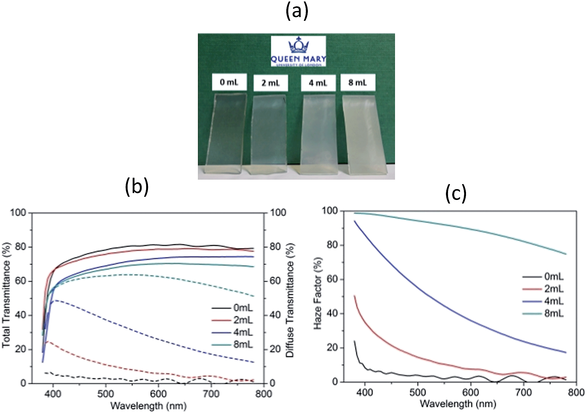 | ||
| Fig. 1 (a) Optical appearance, (b) UV-Vis total and diffuse transmittance and (c) haze factor spectra of ZnO films prepared with various acetic-acid contents in precursor solutions. | ||
To explain this acid-dependent film optical performance, we check the morphology of these zinc oxide coatings by SEM and AFM. As seen in Fig. 2 and S1,† the untreated ZnO is composed by refined spherical grains, with an average size of <50 nm and surface roughness of 12.8 nm, and then turns into agglomerated particles (∼350 nm) after a minor addition of acetic acid to the precursor solution. ZnO grains with pyramid shapes start appearing in S3, in which the angle between two opposite edges was calculated at 63°, only one degree lower than the reported value in {101} faceted pyramids.18 This pyramidal morphology helps increase the surface roughness to 45.1 nm and so more light can be scattered. Moreover, the grains in S3 seem less densely-packed than that in previous two samples, representing a potential decrease of nucleation rate. The ZnO pyramids were further coarsened after the acid content adds to 8 mL and well-shaped grains with six identical side facets are clearly observed. The resulting film surface is ultra-rough, with its RRMS as high as 103 nm, and so strong light trapping effect is obtained. Based on these microstructure observations, we could conclude that (i) the introduction of acetic-acid could alter the ZnO grain size and morphology tremendously, and (ii) the observed opaque film appearance is largely related to their pyramidal surface structures.
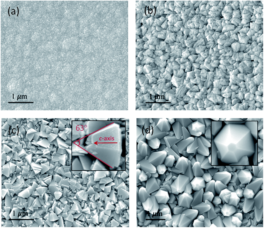 | ||
| Fig. 2 SEM images of ZnO films with (a) 0 mL, (b) 2 mL, (c) 4 mL and (d) 8 mL acetic-acid added in precursor solutions. The insets show higher magnification images for corresponding sample. | ||
The above morphology change can be also reflected by the variations in XRD patterns for present samples. As shown in Fig. 3, besides the diffraction peaks from the substrate SnO2 layer, all other reflection signals can be matched to ZnO with hexagonal wurtzite structure (JCPDS 36-1451).26 Moreover, the untreated sample S1 exhibits an intense peak along the (100) crystallographic plane and this preferential orientation becomes much less significant in S2 since more crystals choose to grow along [101]. The intensity of (101) peak exceeds that of (100) in S3 and S4, which is consistent with the XRD results of pyramid-shaped ZnO in previous studies.19,27 It is noteworthy that, different with the a-axis oriented (100) and c-axis oriented (0001) plane, whose higher XRD peak intensity often means less corresponding surfaces getting exposed, the promotion of (101)-oriented crystal growth will result in larger surface areas and higher diffraction signals together due to its unique symmetry. Thus, combined with the SEM details in Fig. 2, we could conclude that the side facets in our ZnO pyramids are {101} planes. The other interesting information from the XRD pattern is the {0002} diffraction peak in S3 is hardly observed and then become significant in S4, although both surfaces are pyramidal shaped. This transition may originate from a change of crystal packing direction. For example, as shown in Fig. 2(c), the c-axis orientations of ZnO pyramids in S3 are parallel to the substrate, so their (0002)-oriented crystalline atoms cannot be diffracted by the incident X-ray beams. By contrast, the c-axis in the latter specimen S4 is perpendicular or near perpendicular to its surface and thus the {0002} reflection signals are readily collected.
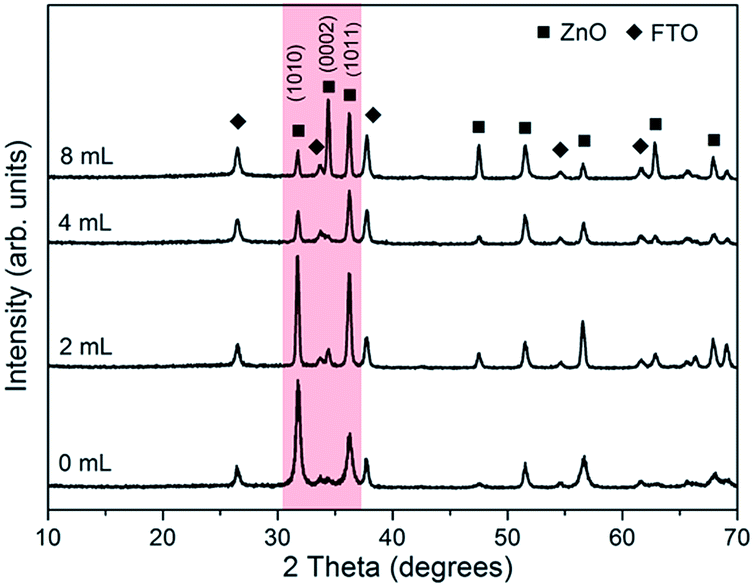 | ||
| Fig. 3 XRD patterns of ZnO films prepared with various acetic-acid contents in precursor solutions. | ||
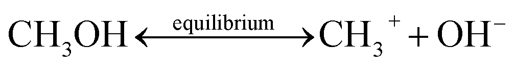
In general, the crystallization procedure of thin films can be divided into the nucleation and grain growth processes. For the current AACVD reaction of ZnO nanomaterials, a plausible crystal nucleation mechanism can be proposed as follows:28–30
 | (1) |
 | (2) |
 | (3) |
 | (4) |
 | (5) |
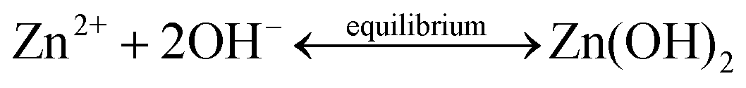
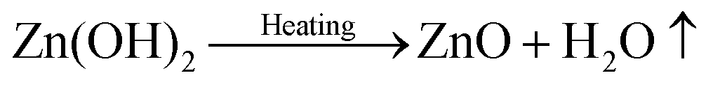
Initially, under the equilibrium solution state, the Zn2+ cations from zinc acetate (eqn (1)) would readily react with the OH− anions from methanol (eqn (2)) to form Zn(OH)2 (eqn (3)). After the aerosol droplets were transported to the heated substrate, the Zn(OH)2 would simultaneously decompose into crystalline ZnO and generate nucleus, whereby the by-products will be removed out of the reactor with the flushing nitrogen gas (eqn (4)). So the number and size of the ZnO nucleus formed are controlled by the concentration of Zn2+ and OH− in precursors and the substrate heating temperature, respectively. Take untreated sample S1 as an example, its small grain size indicates the nucleation rate is extremely high during this deposition. The introduction of acetic-acid in precursor solutions would (i) bring in excess CH3COO− anions (eqn (5)) and reduce the Zn2+ concentration by promoting eqn (1) proceed to left side, and (ii) introduce the OH− scavenger H+, which both can lower the ZnO nucleation rate and decrease the nuclei sites. Thus, the crystals in acid-treated ZnO samples could obtain more lateral space to grow up and their grains are getting increasingly bigger.28 But on the other hand, since less nucleus could form on the substrate especially under a high acid input, the film thickening process in S3 and S4 will be considerably retarded. So these two samples become thinner compared to S1 and S2, as illustrated by their cross-section SEM images in Fig. S2.†
After the initial nucleation, the following grain growth process determines the final film morphology. Typically, the fast-growing surfaces, such as untreated polar facets, exhibit small facets or even disappear during crystal growth because they will be replaced by slower-growing equivalent planes which are observed in the final crystal as the exposed surfaces.19,31 Moreover, as described earlier, organic molecules could incorporate into the crystal lattice of polar facets and hence slowing their growth rate. It is widely known that the carboxylates are often selectively adsorbed on the ZnO surface sites,32 such as citrate bound onto the Zn+-terminated (0001) surface,10,11,33 and different carboxylic acids have been utilized to modify ZnO crystal morphology from nanorods to nanoplates.34 Thus, in our case, the presence of surplus acetate anions may effectively reduce the surface energy of growing {101} planes and promote the formation of ZnO pyramids. Nevertheless, it is still unclear why the acetic-acid selectively function as the growth modifier of {101} surfaces instead of other crystallographic facets. Density-function theory simulation study may provide a better understanding to this.
In conclusion, we fabricate ZnO thin films with ultra-high haze on FTO glass substrate by aerosol assisted chemical vapour deposition. The addition of acetic-acid in precursor solutions could (i) promote lateral grain growth by inhibiting the crystal nucleation, and (ii) expose {101} polar facets by lowering their surface energy, which help form pyramid-like film surface and bring strong light-trapping capability. We believe the AACVD technique can potentially be used to fabricate a wider range of zinc oxide nanostructures with controlled exposed surfaces and morphology.
Acknowledgements
S. Q. Chen would like to thank the China Scholarship Council/Queen Mary University of London joint PhD scholarship program. Pilkington-NSG is specially thanked for providing glass substrates.Notes and references
- S. Chen, N. Noor, I. P. Parkin and R. Binions, J. Mater. Chem. A, 2014, 2, 17174–17182 CAS.
- S. Chen, G. Carraro, D. Barreca and R. Binions, Thin Solid Films, 2014 DOI:10.1016/j.tsf.2014.11.092.
- D. Bekermann, A. Gasparotto, D. Barreca, L. Bovo, A. Devi, R. A. Fischer, O. I. Lebedev, C. Maccato, E. Tondello and G. Van Tendeloo, Cryst. Growth Des., 2010, 10, 2011–2018 CAS.
- N. Qin, Q. Xiang, H. Zhao, J. Zhang and J. Xu, CrystEngComm, 2014, 16, 7062 RSC.
- S. Shoaee, J. Briscoe, J. R. Durrant and S. Dunn, Adv. Mater., 2014, 26, 263–268 CrossRef CAS PubMed.
- Y. H. Leung, Z. B. He, L. B. Luo, C. H. A. Tsang, N. B. Wong, W. J. Zhang and S. T. Lee, Appl. Phys. Lett., 2010, 96, 053102 CrossRef PubMed.
- L. Loh and S. Dunn, J. Nanosci. Nanotechnol., 2012, 12, 8215–8230 CrossRef CAS PubMed.
- J. Liu, X. Chen, W. Wang, Y. Liu, Q. Huang and Z. Guo, CrystEngComm, 2011, 13, 3425 RSC.
- A. McLaren, T. Valdes-Solis, G. Li and S. C. Tsang, J. Am. Chem. Soc., 2009, 131, 12540–12541 CrossRef CAS PubMed.
- Z. R. Tian, J. A. Voigt, J. Liu, B. McKenzie, M. J. McDermott, M. A. Rodriguez, H. Konishi and H. Xu, Nat. Mater., 2003, 2, 821–826 CrossRef CAS PubMed.
- N. J. Nicholas, G. V Franks and W. A. Ducker, Langmuir, 2012, 28, 7189–7196 CrossRef CAS PubMed.
- C. Battaglia, J. Escarré, K. Söderström, M. Charrière, M. Despeisse, F.-J. Haug and C. Ballif, Nat. Photonics, 2011, 5, 535–538 CrossRef CAS.
- Z. Chen, X.-D. Zhang, J.-H. Liang, J. Fang, X.-J. Liang, J. Sun, D.-K. Zhang, X.-L. Chen, Q. Huang and Y. Zhao, Phys. Chem. Chem. Phys., 2014, 17, 459–464 RSC.
- C.-P. Liu, J. Xin, L. Wang, J. Song, A. Y. S. Lee and P. Ho, RSC Adv., 2014, 4, 34669 RSC.
- D. Klauson, I. Gromyko, T. Dedova, N. Pronina, M. Krichevskaya, O. Budarnaja, I. Oja Acik, O. Volobujeva, I. Sildos and K. Utt, Mater. Sci. Semicond. Process., 2015, 31, 315–324 CrossRef CAS PubMed.
- S. Faÿ, L. Feitknecht, R. Schlüchter, U. Kroll, E. Vallat-Sauvain and A. Shah, Sol. Energy Mater. Sol. Cells, 2006, 90, 2960–2967 CrossRef PubMed.
- L. Ding, L. Fanni, D. Messerschmidt, S. Zabihzadeh, M. M. Masis, S. Nicolay and C. Ballif, Sol. Energy Mater. Sol. Cells, 2014, 128, 378–385 CrossRef CAS PubMed.
- T. Shinagawa, K. Shibata, O. Shimomura, M. Chigane, R. Nomura and M. Izaki, J. Mater. Chem. C, 2014, 2, 2908 RSC.
- X. Zhou, Z.-X. Xie, Z.-Y. Jiang, Q. Kuang, S.-H. Zhang, T. Xu, R.-B. Huang and L.-S. Zheng, Chem. Commun., 2005, 5572–5574 RSC.
- R. Elleuch, R. Salhi, N. Maalej, J.-L. Deschanvres and R. Maalej, Mater. Sci. Eng. B, 2013, 178, 1124–1129 CrossRef CAS PubMed.
- P. Marchand, I. A. Hassan, I. P. Parkin and C. J. Carmalt, Dalton Trans., 2013, 9406–9422 RSC.
- S. Ponja, S. Sathasivam, N. Chadwick, A. Kafizas, S. M. Bawaked, A. Y. Obaid, S. Al-Thabaiti, S. N. Basahel, I. P. Parkin and C. J. Carmalt, J. Mater. Chem. A, 2013, 1, 6271 CAS.
- N. Noor and I. P. Parkin, J. Mater. Chem. C, 2013, 1, 984 RSC.
- P. F. Cai, J. B. You, X. W. Zhang, J. J. Dong, X. L. Yang, Z. G. Yin and N. F. Chen, J. Appl. Phys., 2009, 105, 083713 CrossRef PubMed.
- J.-M. Lee, K.-K. Kim, S.-J. Park and W.-K. Choi, Appl. Phys. Lett., 2001, 78, 3842 CrossRef CAS PubMed.
- Joint Committee Powder Diffraction Standards, Powder Diffraction File (Data File 36-1451).
- Q. Kuang, X. Zhou and L.-S. Zheng, Inorg. Chem. Front., 2014, 1, 186 RSC.
- T. Shinagawa and M. Izaki, RSC Adv., 2014, 4, 30999 RSC.
- S. Yamabi and H. Imai, J. Mater. Chem., 2002, 3773–3778 RSC.
- H. Yin, Z. Xu, Q. Wang, J. Bai and H. Bao, Mater. Chem. Phys., 2005, 91, 130–133 CrossRef CAS PubMed.
- N. P. Herring, K. AbouZeid, M. B. Mohamed, J. Pinsk and M. S. El-Shall, Langmuir, 2011, 27, 15146–15154 CrossRef CAS PubMed.
- K. Govender, D. S. Boyle, P. B. Kenway and P. O. Brien, J. Mater. Chem., 2004, 14, 2575–2591 RSC.
- B. D. Andeen, J. H. Kim, F. F. Lange, G. K. L. Goh and S. Tripathy, Adv. Funct. Mater., 2006, 799–804 CrossRef.
- J. Yahiro, T. Kawano and H. Imai, J. Colloid Interface Sci., 2007, 310, 302–311 CrossRef CAS PubMed.
Footnote |
| † Electronic supplementary information (ESI) available. See DOI: 10.1039/c5ta00446b |
| This journal is © The Royal Society of Chemistry 2015 |