 Open Access Article
In situ growth of CuS and Cu1.8S nanosheet arrays as efficient counter electrodes for quantum dot-sensitized solar cells†
Meidan
Ye
a,
Xiaoru
Wen
b,
Nan
Zhang
b,
Wenxi
Guo
a,
Xiangyang
Liu
a and
Changjian
Lin
*ab
aResearch Institute for Soft Matter and Biomimetics, Department of Physics, School of Physics and Mechanical & Electrical Engineering, Xiamen University, Xiamen, 361005, China. E-mail: cjlin@xmu.edu.cn
bState Key Laboratory of Physical Chemistry of Solid Surfaces, Department of Chemistry, College of Chemistry and Chemical Engineering, Xiamen University, Xiamen, 361005, China
First published on 16th March 2015
Abstract
Vertical CuS nanosheet arrays were synthesized in situ for the first time on transparent conducting fluorine-doped tin oxide (FTO) substrates via a facile solvothermal process of seeded FTO glasses in the presence of ethanol solvent only containing thiourea and Cu(NO3)2 as a precursor. While choosing CuCl instead of Cu(NO3)2 as the copper precursor in the same solvothermal process, porous Cu1.8S nanosheets, for the first time, were also vertically grown on FTO substrates, suggesting that such a synthesis process is a general approach for the preparation of copper sulfide nanosheet arrays. When used as low-cost counter electrode materials in quantum dot-sensitized solar cells (QDSSCs), CuS (3.95%) and Cu1.8S (3.30%) nanosheet films exhibited enhanced power conversion efficiencies in comparison with the conventional Pt film (1.99%), which was primarily due to the excellent electrocatalytic activity of copper sulfides for the reduction of the polysulfide electrolyte used in CdSe/CdS QDSSCs. Significantly, the in situ growth strategy largely simplified the fabrication procedure of copper sulfide counter electrodes and, meanwhile, enhanced the adhesion between films and substrates.
1. Introduction
In the past years, semiconductor metal sulfides, especially CdS, PbS, ZnS, CuS and CoS, have attracted extensive attention because of their attractive physical and chemical properties for potential applications in many fields.1–4 In particular, copper sulfides (CuxS, x = 1–2) have aroused considerable interest due to their variations in stoichiometric composition, valence states, complex structures, and different unique properties.5–7 Copper sulfides have different stoichiometric forms, including at least five stable phases at room temperature: covellite (CuS) at the copper-deficient side, anilite (Cu1.75S), digenite (Cu1.8S), djurleite (Cu1.97S), and chalcocite (Cu2S) at the copper-rich side.8–11 Copper sulfides with different stoichiometries show prospective applications in solar cells, photocatalysis, photo-thermal conversion, sensors, lithium rechargeable batteries, etc.12–16 Significantly, copper sulfides, owing to their low cost, environmental friendliness and various band-gap energies in a range of 1.2–2.0 eV, are considered as one of the most promising materials for the future sustainable energy supply.17,18Recently, the fine control of nanomaterials with versatile chemical composition, crystal structure, size, shape and surface chemistry has attracted increasing attention, mainly due to their ability to modulate the optical, electronic and catalytic response of materials, and then show important technological applications as advanced materials with unique properties.19–21 Copper sulfides with various morphologies, such as nanoplates,20 nanosheets,22 hollow spheres,3 nanoparticles,23–25 nanowires,21,26,27 tubular structures,28 flower-like,29,30 hierarchical nanostructures,8,31,32etc., have been obtained via many synthesis routes, including the successive ionic layer adsorption and reaction (SILAR) method,2 wet chemical bath,13 sol–gel method,9,19 hydrothermal or solvothermal process,33,34 mechanical alloying and spark plasma sintering technique,14 chemical vapor deposition,35,36 atomic layer deposition,37 microemulsion approach,11 and an in situ template-controlled method.38 For example, Kim et al. used single-crystalline wurtzite CdS nanowires that underwent gas-phase substitution to form unique superlattice cubic Cu1.8S and hexagonal Cu2S nanowires through thermal evaporation of CuCl2 at 500–600 °C.26 Feldmann et al. prepared CuS, Cu1.8S and Cu2S hollow spheres via a microemulsion route by adjusting the experimental conditions.11 Xu et al. chose Cu2O crystals with various well-defined morphologies, such as cubic, octahedral and star-like shapes, as the sacrificial templates to prepare copper sulfide materials, which could be tuned from Cu2S to Cu1.75S by controlling the reaction conditions from N2 to air atmospheres, respectively.38 However, there are few reports about the synthesis of copper sulfide nanostructures directly grown on conductive substrates to simplify the preparation process of electrodes.
In this regard, fluorine-doped tin oxide (FTO) glasses were deposited with CuS seeds by the spin coating method and subsequently set in Teflon-lined autoclaves only containing thiourea and Cu(NO3)2 ethanol solution as the precursor to grow CuS nanosheet arrays on the pre-treated FTO substrates. When using CuCl as the copper source, rough Cu1.8S nanosheet films were successfully developed from the seeded FTO substrates. Since copper sulfides are regarded as one of the most efficient counter electrode materials in QDSSCs, it was found that the as-prepared CuS and Cu1.8S nanosheets had superior electrocatalytic activity for the reduction of the polysulfide electrolyte compared to the conventional Pt films, which in turn reflected enhanced power conversion efficiencies of QDSSCs.
2. Experimental section
2.1 Fabrication of CuS and Cu1.8S nanosheet arrays
The FTO substrate (F![[thin space (1/6-em)]](https://www.rsc.org/images/entities/char_2009.gif) :
:![[thin space (1/6-em)]](https://www.rsc.org/images/entities/char_2009.gif) SnO2, 0.5 cm × 1.2 cm) was ultrasonically cleaned for 15 min in a mixed solution of acetone and ethanol (v/v, 1
SnO2, 0.5 cm × 1.2 cm) was ultrasonically cleaned for 15 min in a mixed solution of acetone and ethanol (v/v, 1![[thin space (1/6-em)]](https://www.rsc.org/images/entities/char_2009.gif) :
:![[thin space (1/6-em)]](https://www.rsc.org/images/entities/char_2009.gif) 1), followed by deionized water rinsing for 15 min. CuS seeds were planted on the cleaned FTO substrate via spin coating by alternating 0.01 M Cu(NO3)2 and 0.01 M Na2S aqueous solution three times. The seeded FTO substrate was placed in a Teflon-lined stainless steel autoclave (50 mL) containing 40 mL ethanol with 0.05 M Cu(NO3)2 and 0.1 M thiourea. The solvothermal reaction was performed at 150 °C for 24 h in an oven. When the autoclave was cooled to room temperature, the FTO substrate was taken out, rinsed with ethanol, and dried in air. Then, CuS nanosheet arrays grown on the FTO substrate were obtained. For the Cu1.8S nanosheet film, CuCl was alternatively employed as the copper source in a similar solvothermal reaction.
1), followed by deionized water rinsing for 15 min. CuS seeds were planted on the cleaned FTO substrate via spin coating by alternating 0.01 M Cu(NO3)2 and 0.01 M Na2S aqueous solution three times. The seeded FTO substrate was placed in a Teflon-lined stainless steel autoclave (50 mL) containing 40 mL ethanol with 0.05 M Cu(NO3)2 and 0.1 M thiourea. The solvothermal reaction was performed at 150 °C for 24 h in an oven. When the autoclave was cooled to room temperature, the FTO substrate was taken out, rinsed with ethanol, and dried in air. Then, CuS nanosheet arrays grown on the FTO substrate were obtained. For the Cu1.8S nanosheet film, CuCl was alternatively employed as the copper source in a similar solvothermal reaction.
2.2 Preparation of CdS/CdSe QDSSCs
For QDSSCs, hierarchical TiO2 spheres reported in our previous work were used as the photoanode material.39 The photoanode films with a thickness of about 20 μm were obtained by coating the hierarchical TiO2 sphere paste on FTO glasses using the doctor blade method. After a calcination process at 450 °C for 30 min to remove the organic substances, the TiO2 films were soaked in 0.2 M TiCl4 aqueous solution at 70 °C for 40 min followed by calcination at 450 °C for 30 min.To fabricate CdS/CdSe QDSSCs, deposition of CdS and CdSe QDs onto the TiO2 photoanodes was realized by the chemical bath deposition (CBD) technique in a refrigerator with temperature at 10 °C.40 CdS QDs were deposited in an aqueous solution containing 20 mM CdCl2, 66 mM NH4Cl, 140 mM thiourea, and 230 mM ammonia (pH = 9.5) for 80 min. The deposition of CdSe QDs was subsequently carried out in a mixture of Na2SeSO3 solution and 0.08 M Cd(NO3)2 solution with a volume ratio of 1![[thin space (1/6-em)]](https://www.rsc.org/images/entities/char_2009.gif) :
:![[thin space (1/6-em)]](https://www.rsc.org/images/entities/char_2009.gif) 1 for 30 h. The Na2SeSO3 aqueous solution used was prepared by dissolving Se (0.1 M) in an aqueous solution of Na2SO3 (0.18 M) at 70 °C for about 7 h when the black Se powder was almost reacted. After cooling to room temperature, the obtained Na2SeSO3 aqueous solution was filtered to remove the unreacted Se powder.
1 for 30 h. The Na2SeSO3 aqueous solution used was prepared by dissolving Se (0.1 M) in an aqueous solution of Na2SO3 (0.18 M) at 70 °C for about 7 h when the black Se powder was almost reacted. After cooling to room temperature, the obtained Na2SeSO3 aqueous solution was filtered to remove the unreacted Se powder.
CdS/CdSe sensitized TiO2 films with an active area of about 0.20 cm2 were assembled together with the above-prepared CEs by applying a 60 μm thick hot-melt sealed film as the spacer (SX1170-25; Solaronix Co.). The polysulfide electrolyte used here consists of 3.5 mL DI water and 1.5 mL methanol with 0.5 M Na2S, 0.125 M S and 0.2 M KCl. The electrolyte was injected between two electrodes and driven by the capillary force through the hole on the hot-melt sealed film.16,41
2.3 Characterization
The morphology of the samples was observed by field emission scanning electron microscopy (FESEM, HITACHI S-4800) and transmission electron microscopy (TEM, JEOL JEM-2100) with an acceleration voltage of 200 kV. Phase identification of materials was carried out by X-ray diffraction (XRD, Panalytical X'pert PRO). The X-ray photoelectron spectroscopy (XPS) analysis was carried out with a Quantum 2000 Scanning ESCA Microprobe spectrometer using focused monochromatized Al Kα radiation (1486.6 eV). The performance of the as-prepared DSSCs was determined by measuring photocurrent density–photovoltage (J–V) curves under AM 1.5G simulated solar light (Oriel 300 W Xe lamp and Newport AM-1.5G filter). The incident-photon-to-current efficiency (IPCE) spectra as a function of wavelength (λ = 300 to 800 nm) were recorded using a monochromator (Oriel, Model: 74125). The cyclic voltammogram (CV) was obtained on an Autolab electrochemical workstation in a three-electrode system with counter electrodes as the working electrodes, a Pt foil as the counter electrode, and an SCE as the reference electrode at a scan rate of 50 mV s−1. The electrolyte was 70 mL DI water and 30 mL methanol with 0.5 M Na2S, 0.125 M S and 0.2 M KCl. The charge transfer resistance was determined by electrochemical impedance spectroscopy (EIS), performed on the symmetric cells using an Autolab electrochemical workstation under an open circuit voltage (0 V) over a frequency range of 105 to 10−1 Hz with an AC voltage magnitude of 10 mV. The impedance data were analyzed using Autolab electrochemical EIS fitting software. The electrochemical workstation was also employed to measure the Tafel-polarization curves of the symmetric cells at a scan rate of 5 mV s−1.3. Results and discussion
As shown in Fig. 1a, the XRD pattern revealed that the CuS (JCPDS no. 06-0464) film was obtained via solvothermally treating the seeded FTO substrate in the ethanol containing 0.05 M Cu(NO3)2 and 0.1 M thiourea at 150 °C for 24 h. The product had XRD diffraction peaks at 2θ = 27.1°, 27.6°, 29.2°, 31.7°, 32.8°, 47.9° and 59.3°, corresponding to those of lattice planes (100), (101), (102), (103), (006), (110) and (116) of the hexagonal CuS phase. In addition, if the copper source is changed in the reaction solution from Cu(NO3)2 to CuCl, under the same solvothermal conditions, the resulting product can be indexed to Cu1.8S (JCPDS no. 24-0061) with diffraction peaks observed at 2θ = 27.7°, 32.1°, 46.1° and 54.6°, associating with those of the lattice planes (111), (200), (220) and (311) of the cubic Cu1.8S phase (Fig. 1b). Since the CuS and Cu1.8S films were thin (∼1 μm), the XRD signals of FTO substrates were strong (Fig. 1).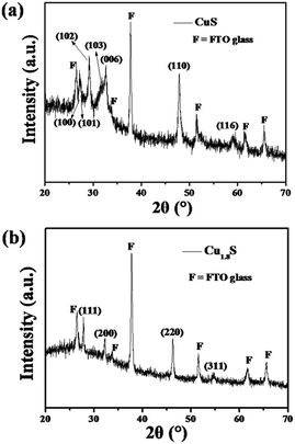 | ||
| Fig. 1 XRD patterns of (a) CuS and (b) Cu1.8S nanosheet films prepared via the solvothermal process. | ||
Fig. 2 shows SEM images of the CuS and Cu1.8S films indexed by XRD patterns in Fig. 1. As shown in Fig. 2a and b, the CuS film consisted of well-defined nanosheet arrays, and the vertical CuS nanosheets randomly intercrossed with each other and well uniformly grew on the FTO substrate. It was observed that such CuS nanosheets were smooth with a thickness of about 10 nm (Fig. 2b). For the Cu1.8S film, similar nanosheet arrays were successfully planted on the FTO substrate (Fig. 2c and d). Compared to CuS nanosheets (Fig. 2b), Cu1.8S nanosheets were relatively rough with a thickness of around 50 nm (Fig. 2d). Obviously, the type of copper salt used in the solvothermal reaction had a great impact on the shape and crystal phase of the products.
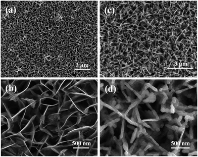 | ||
| Fig. 2 SEM images of (a) CuS and (c) Cu1.8S nanosheet films; (b) and (d) are the magnified images of (a) and (d), respectively. | ||
To further study the detailed structures of the products, the TEM measurement was subsequently performed. The obtained TEM images also revealed that the CuS nanosheet had a smooth surface (Fig. 3a), while the Cu1.8S nanosheet was rough (Fig. 3c). These two types of nanosheets were completely crystalline as proved by the HRTEM images (Fig. 3b and d). Lattice fringes with interplanar spacings d102 = 0.304 nm (Fig. 3b) and d200 = 0.279 nm (Fig. 3d) can be indexed to the hexagonal CuS phase and cubic Cu1.8S phase, respectively. The corresponding SAED patterns (insets of Fig. 3b and d) of the CuS and Cu1.8S nanosheets demonstrated that they were single crystals with great crystallinity. In addition, the corresponding EDX results are shown in Fig. S1.† The ratios of Cu and S atoms for CuS and Cu1.8S nanosheets were 1.002![[thin space (1/6-em)]](https://www.rsc.org/images/entities/char_2009.gif) :
:![[thin space (1/6-em)]](https://www.rsc.org/images/entities/char_2009.gif) 1 and 1.787
1 and 1.787![[thin space (1/6-em)]](https://www.rsc.org/images/entities/char_2009.gif) :
:![[thin space (1/6-em)]](https://www.rsc.org/images/entities/char_2009.gif) 1, respectively, which were almost the same as 1
1, respectively, which were almost the same as 1![[thin space (1/6-em)]](https://www.rsc.org/images/entities/char_2009.gif) :
:![[thin space (1/6-em)]](https://www.rsc.org/images/entities/char_2009.gif) 1 and 1.8
1 and 1.8![[thin space (1/6-em)]](https://www.rsc.org/images/entities/char_2009.gif) :
:![[thin space (1/6-em)]](https://www.rsc.org/images/entities/char_2009.gif) 1.
1.
 | ||
| Fig. 3 TEM and HRTEM images of (a and b) CuS and (c and d) Cu1.8S nanosheet films, and insets are the corresponding SAED patterns of (b) and (d), respectively. | ||
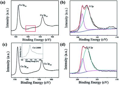
XPS analysis was carried out to investigate the chemical binding states of the as-prepared CuS and Cu1.8S nanosheets. Fig. 4a shows the XPS spectrum of Cu 2p for CuS nanosheets. The two main peaks located at 931.9 and 951.9 eV (Fig. 4a) were assigned to Cu 2p3/2 and Cu 2p1/2, respectively. Moreover, there were weak shake-up satellite peaks at around 943 eV (rectangle marked in Fig. 4a), suggesting the presence of the paramagnetic chemical state of Cu2+.42 The corresponding XPS spectrum of S 2p for CuS nanosheets is shown in Fig. 4b. In the case of the XPS spectrum of Cu 2p for Cu1.8S nanosheets, the Cu 2p3/2 and Cu 2p1/2 peaks were observed at 932.1 and 952.1 eV (Fig. 4c), respectively. Noticeably, the accompanying Auger line (Cu LMM) at 568.6 eV (inset in Fig. 4c) indicated that the Cu ion was in the form of the Cu(I) state, implying that the chemical binding state of Cu1.8S was close to Cu2S.42 Also, Fig. 4d shows the corresponding XPS spectrum of S 2p for Cu1.8S nanosheets.
In the control experiments, it was found that the CuS seeds on FTO substrates promoted the successful growth of copper sulfide nanosheet arrays. When the FTO substrate was absent of seeding treatment, after the solvothermal reaction in ethanol containing the same precursor, no film was formed and only some microsphere products were dispersed on the FTO substrate (Fig. S2a†). When employing the drop-cast method to prepare CuS seeds on the FTO substrate, a CuS nanosheet film was obtained after the same solvothermal reaction (Fig. S2b†). However, the quality of such a CuS nanosheet film was poor. Then, the CuS seeds prepared via spin coating led to the successful fabrication of vertical copper sulfide nanosheet arrays with high quality as shown in Fig. 2. In addition, adjusting solvothermal conditions, such as precursor concentration (Fig. S3a†), reaction temperature (Fig. S3b and S4a†) and growth time (Fig. S4b†), remarkably influenced the features of copper sulfide nanosheet arrays.
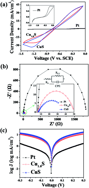
The CuS and Cu1.8S nanosheet arrays grown on FTO substrates (Fig. 2) were then applied as counter electrodes (CEs) to assemble CdS/CdSe QDSSCs (Experimental section). Table 1 summarizes the photovoltaic parameters of the resulting QDSSCs and Fig. 5a shows the corresponding current–voltage (J–V) characteristics. Using the Pt CE-based QDSSC as a reference, largely enhanced photovoltaic performance of the QDSSCs employing CuS and Cu1.8S nanosheets as CEs was finally obtained (Table 1). In comparison with Pt CEs, CuS and Cu1.8S nanosheet CEs endowed the cells with a higher short circuit current density (Jsc; Pt: 13.31 mA cm−2νs. Cu1.8S: 16.07 mA cm−2 and CuS: 15.08 mA cm−2) and fill factor (FF; Pt: 0.30 νs. Cu1.8S: 0.41 and CuS: 0.51), and thus obviously improved power conversion efficiency (PCE; Pt: 1.99% νs. Cu1.8S: 3.30% and CuS: 3.95%) for assembling QDSSCs. Therefore, it was indicated that these CuS and Cu1.8S nanosheet arrays had better electrocatalytic ability for the polysulfide reduction. In addition, CuS nanosheet arrays exhibited a higher PCE value than that of Cu1.8S nanosheet arrays for the corresponding QDSSCs; this was probably because the crystal phase of CuS nanosheets matched well with that of CuS seeds, and then the CuS nanosheet film with fewer structure defects had better contact with the FTO substrate. However, the rough Cu1.8S nanosheets had a slightly higher Jsc value partially since they had larger surface areas to give more catalytic sites for the polysulfide reduction. Furthermore, we also prepared the Cu2S/brass CE and its corresponding QDSSC. As shown in Fig. S5a,† the cell efficiency of Cu2S/brass CEs can be up to 3.12%, but it quickly decreased to 0.65% after 1–2 hours because of the exfoliation of the Cu2S film from brass. For other kinds of CEs, after several tests, CuS and Cu1.8S CEs showed higher stability as compared to Pt and Cu2S CEs (Fig. S5†).
| Sample | J sc (mA cm−2) | V oc (V) | FF | PCE (%) | R s (Ω) | R CT (Ω) |
|---|---|---|---|---|---|---|
| Pt | 13.31 | 0.50 | 0.30 | 1.99 | 6.21 | 1836 |
| Cu1.8S | 16.07 | 0.50 | 0.41 | 3.30 | 6.11 | 44.34 |
| CuS | 15.08 | 0.51 | 0.51 | 3.95 | 6.53 | 33.36 |
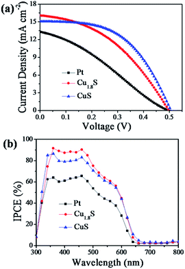 | ||
| Fig. 5 (a) J–V curves and (b) IPCE spectra of the QDSSCs based on Pt, CuS and Cu1.8S counter electrodes. | ||
Fig. 5b shows the incident photon-to-current efficiency (IPCE) spectra recorded to scrutinize the different photovoltaic performances of the QDSSCs based on Pt, Cu1.8S and CuS CEs. The IPCE spectra of Cu1.8S and CuS-based QDSSCs were both higher over almost the tested wavelength region (300–800 nm) as compared to Pt-based QDSSCs; moreover, the IPCE spectra of the Cu1.8S-based QDSSCs were slightly higher than those of the CuS-based QDSSCs. The IPCE results agreed well with the aforementioned Jsc values of the three QDSSCs (Table 1). The improved Jsc values of Cu1.8S and CuS-based QDSSCs were mainly attributed to their greater electrocatalytic ability for the polysulfide reduction, which was further confirmed by the following electrochemical analysis, namely, cyclic voltammetry (CV), electrochemical impedance spectroscopy (EIS) and Tafel polarization measurements.
The CV analysis was applied to investigate the electrochemical electrocatalytic activity of these three electrodes. Generally, the negative currents of CV plots represent the reduction of Sx2− ions to S2− ions while their positive currents are related to the oxidation of S2− ions in the polysulfide electrolyte. As the CE materials in QDSSCs, the reduction peak currents of CV plots of the electrodes directly reflect the electrocatalytic ability of the CEs for Sx2− reduction.43 Accordingly, the Cu1.8S and CuS nanosheet electrodes (Fig. 6a) with considerably higher current densities at the reduction peaks of CV plots in comparison with the Pt electrode (inset of Fig. 6a) had superior electrocatalytic ability for Sx2− reduction. Meanwhile, CuS electrodes with a better crystal structure exhibited a higher reduction peak current than that of Cu1.8S electrodes.
Furthermore, Fig. 6b shows the EIS spectra of symmetric cells organized by Pt, Cu1.8S and CuS CEs, respectively. After fitting the experimental data via the equivalent circuit (inset in Fig. 6b), the resulting Nyquist plots of EIS spectra showed one semicircle which was associated with the charge-transfer resistance (RCT) and the interfacial capacitance (CPE) at the CE/electrolyte interface.44 As shown in Table 1, the RCT value of the Pt CE was very large, confirming its poor electrocatalytic activity in the polysulfide electrolyte. The CuS electrode had a smaller RCT value than that of the Cu1.8S electrode, which was mainly because the formed CuS nanosheets had fewer structure defects and better contact with the FTO substrate.
In addition, Tafel-polarization analysis was performed using the same symmetric cells in the above EIS measurement. As shown in Fig. 6c, the Tafel polarization curve is the logarithmic current density (log![[thin space (1/6-em)]](https://www.rsc.org/images/entities/char_2009.gif) J) as a function of the voltage (V). The exchange current density (Jo) of samples can be evaluated as the intercept of the extrapolated linear region of anodic and cathodic branches when the voltage is zero. Moreover, the Jo can also be calculated by the following equation: Jo = RT/nFRCT.45,46 Therefore, the higher the Jo value, the lower the RCT value. It was observed that the CuS electrode had the highest Jo value with the lowest RCT value, suggesting the best electrocatalytic activity, in good agreement with the CV and EIS results.
J) as a function of the voltage (V). The exchange current density (Jo) of samples can be evaluated as the intercept of the extrapolated linear region of anodic and cathodic branches when the voltage is zero. Moreover, the Jo can also be calculated by the following equation: Jo = RT/nFRCT.45,46 Therefore, the higher the Jo value, the lower the RCT value. It was observed that the CuS electrode had the highest Jo value with the lowest RCT value, suggesting the best electrocatalytic activity, in good agreement with the CV and EIS results.
4. Conclusion
The seed assisted-solvothermal process has been exploited for the first time to develop vertical CuS and Cu1.8S nanosheet arrays directly grown on FTO substrates. The type of copper salt used in the solvothermal reaction remarkably influenced the crystal phases and features of the resulting products. The obtained CuS and Cu1.8S nanosheet arrays exhibited enhanced PCEs up to 3.95% and 3.30% when used as CEs in QDSSCs, implying increases of 98% and 66% as compared to Pt-based QDSSCs, respectively. Such a synthesis strategy not only simplified the preparation procedure of CEs, but also achieved efficient QDSSC devices based on the formed copper sulfide CEs.Acknowledgements
The authors gratefully acknowledge the financial support from the National Basic Research Program of China (2012CB932900), and the National Natural Science Foundation of China (21321062).Notes and references
- L. Bakueva, I. Gorelikov, S. Musikhin, X. S. Zhao, E. H. Sargent and E. Kumacheva, Adv. Mater., 2004, 16, 926–929 CrossRef CAS.
- N. Balis, V. Dracopoulos, K. Bourikas and P. Lianos, Electrochim. Acta, 2013, 91, 246–252 CrossRef CAS PubMed.
- J. Gao, Q. Li, H. Zhao, L. Li, C. Liu, Q. Gong and L. Qi, Chem. Mater., 2008, 20, 6263–6269 CrossRef CAS.
- W. Guo, C. Chen, M. Ye, M. Lv and C. Lin, Nanoscale, 2014, 6, 3656–3663 RSC.
- I. Grozdanov and M. Najdoski, J. Solid State Chem., 1995, 114, 469–475 CrossRef CAS.
- Q. Lu, F. Gao and D. Zhao, Nano Lett., 2002, 2, 725–728 CrossRef CAS.
- X. L. Yu, C. B. Cao, H. S. Zhu, Q. S. Li, C. L. Liu and Q. H. Gong, Adv. Funct. Mater., 2007, 17, 1397–1401 CrossRef CAS.
- B. Li, Y. Xie and Y. Xue, J. Phys. Chem. C, 2007, 111, 12181–12187 CAS.
- X. Zheng, Z. Jin, H. Liu, Y. Wang, X. Wang and H. Du, Appl. Surf. Sci., 2013, 266, 39–45 CrossRef CAS PubMed.
- W. Georg, E. Hinze and A. R. M. Abdelrahman, Eur. J. Mineral., 2002, 14, 591–598 CrossRef.
- P. Leidinger, R. Popescu, D. Gerthsen, H. Lünsdorf and C. Feldmann, Nanoscale, 2011, 3, 2544–2551 RSC.
- M.-C. Lin and M.-W. Lee, Electrochem. Commun., 2011, 13, 1376–1378 CrossRef CAS PubMed.
- M. Basu, A. K. Sinha, M. Pradhan, S. Sarkar, Y. Negishi and T. Pal, Environ. Sci. Technol., 2010, 44, 6313–6318 CrossRef CAS PubMed.
- Z.-H. Ge, B.-P. Zhang, Y.-X. Chen, Z.-X. Yu, Y. Liu and J.-F. Li, Chem. Commun., 2011, 47, 12697–12699 RSC.
- H. Lee, S. W. Yoon, E. J. Kim and J. Park, Nano Lett., 2007, 7, 778–784 CrossRef CAS PubMed.
- M. Ye, C. Chen, N. Zhang, X. Wen, W. Guo and C. Lin, Adv. Energy Mater., 2014, 4, 1301564 Search PubMed.
- L. Isac, A. Duta, A. Kriza, S. Manolache and M. Nanu, Thin Solid Films, 2007, 515, 5755–5758 CrossRef CAS PubMed.
- Y. Wu, C. Wadia, W. Ma, B. Sadtler and A. P. Alivisatos, Nano Lett., 2008, 8, 2551–2555 CrossRef CAS PubMed.
- X. Liu, X. Wang, B. Zhou, W. C. Law, A. N. Cartwright and M. T. Swihart, Adv. Funct. Mater., 2012, 23, 1256–1264 CrossRef.
- P. Kumar, M. Gusain and R. Nagarajan, Inorg. Chem., 2011, 50, 3065–3070 CrossRef CAS PubMed.
- H.-X. Zhang, J.-P. Ge, J. Wang and Y.-D. Li, Nanotechnology, 2006, 17, S253 CrossRef CAS.
- Y. Lei, H. Jia, Z. Zheng, Y. Gao, X. Chen and H. Hou, CrystEngComm, 2011, 13, 6212–6217 RSC.
- W. Li, A. Shavel, R. Guzman, J. Rubio-Garcia, C. Flox, J. Fan, D. Cadavid, M. Ibáñez, J. Arbiol and J. R. Morante, Chem. Commun., 2011, 47, 10332–10334 RSC.
- H. Zhang, Y. Zhang, J. Yu and D. Yang, J. Phys. Chem. C, 2008, 112, 13390–13394 CAS.
- Z. Zhuang, Q. Peng, B. Zhang and Y. Li, J. Am. Chem. Soc., 2008, 130, 10482–10483 CrossRef CAS PubMed.
- H. S. Kim, T. K. Sung, S. Y. Jang, Y. Myung, Y. J. Cho, C.-W. Lee, J. Park, J.-P. Ahn, J.-G. Kim and Y.-J. Kim, CrystEngComm, 2011, 13, 2091–2095 RSC.
- P. Roy and S. K. Srivastava, Cryst. Growth Des., 2006, 6, 1921–1926 CAS.
- X. Zheng and Q. Hu, Appl. Phys. A, 2009, 94, 805–812 CrossRef CAS.
- Z. Nan, X.-Y. Wang and Z. Zhao, J. Cryst. Growth, 2006, 295, 92–96 CrossRef CAS PubMed.
- A.-M. Qin, Y.-P. Fang, H.-D. Ou, H.-Q. Liu and C.-Y. Su, Cryst. Growth Des., 2005, 5, 855–860 CAS.
- F. Li, W. Bi, T. Kong and Q. Qin, Cryst. Res. Technol., 2009, 44, 729–735 CrossRef CAS.
- J. Xu, X. Yang, T.-L. Wong and C.-S. Lee, Nanoscale, 2012, 4, 6537–6542 RSC.
- L. Ge, X.-Y. Jing, J. Wang, S. Jamil, Q. Liu, D.-L. Song, J. Wang, Y. Xie, P.-P. Yang and M.-L. Zhang, Cryst. Growth Des., 2010, 10, 1688–1692 CAS.
- Y. Zhao, H. Pan, Y. Lou, X. Qiu, J. Zhu and C. Burda, J. Am. Chem. Soc., 2009, 131, 4253–4261 CrossRef CAS PubMed.
- J. P. Ge, J. Wang, H. X. Zhang and Y. D. Li, Chem.–Eur. J., 2004, 10, 3525–3530 CrossRef CAS PubMed.
- M. Xu, H. Wu, P. Da, D. Zhao and G. Zheng, Nanoscale, 2012, 4, 1794–1799 RSC.
- L. Reijnen, B. Meester, F. de Lange, J. Schoonman and A. Goossens, Chem. Mater., 2005, 17, 2724–2728 CrossRef CAS.
- S. Jiao, L. Xu, K. Jiang and D. Xu, Adv. Mater., 2006, 18, 1174–1177 CrossRef CAS.
- M. Ye, C. Chen, M. Lv, D. Zheng, W. Guo and C. Lin, Nanoscale, 2013, 5, 6577–6583 RSC.
- X.-F. Guan, S.-Q. Huang, Q.-X. Zhang, X. Shen, H.-C. Sun, D.-M. Li, Y.-H. Luo, R.-C. Yu and Q.-B. Meng, Nanotechnology, 2011, 22, 465402 CrossRef PubMed.
- M. D. Ye, X. K. Xin, C. J. Lin and Z. Q. Lin, Nano Lett., 2011, 11, 3214–3220 CrossRef CAS PubMed.
- M. Lee and K. Yong, Nanotechnology, 2012, 23, 194014 CrossRef PubMed.
- J. G. Radich, R. Dwyer and P. V. Kamat, J. Phys. Chem. Lett., 2011, 2, 2453–2460 CrossRef CAS.
- Y. Yang, L. Zhu, H. Sun, X. Huang, Y. Luo, D. Li and Q. Meng, ACS Appl. Mater. Interfaces, 2012, 4, 6162–6168 CAS.
- J. Dong, S. Jia, J. Chen, B. Li, J. Zheng, J. Zhao, Z. Wang and Z. Zhu, J. Mater. Chem., 2012, 22, 9745–9750 RSC.
- W. Guo, Y. Shen, M. Wu, L. Wang and T. Ma, Chem.–Eur. J., 2012, 18, 7862–7868 CrossRef CAS PubMed.
Footnote |
| † Electronic supplementary information (ESI) available: FESEM images of copper sulfide films prepared in other control experiments. See DOI: 10.1039/c5ta00390c |
| This journal is © The Royal Society of Chemistry 2015 |

