
 Open Access Article
 This Open Access Article is licensed under a Creative Commons Attribution-Non Commercial 3.0 Unported Licence
Systematic increase of electrocatalytic turnover at nanoporous platinum surfaces prepared by atomic layer deposition†
Loïc
Assaud‡
*a,
Johannes
Schumacher§
a,
Alexander
Tafel
a,
Sebastian
Bochmann
a,
Silke
Christiansen
bc and
Julien
Bachmann
*a
aFriedrich-Alexander University Erlangen-Nürnberg, Department of Chemistry and Pharmacy, Egerlandstrasse 1, 91058 Erlangen, Germany. E-mail: loic.assaud@ensiacet.fr; julien.bachmann@fau.de
bMax Planck Institute for the Science of Light, Günther-Scharowsky-Strasse 1, 91058 Erlangen, Germany
cHelmholtz-Center Berlin (HZB), Hahn-Meitner-Platz 1, 14109 Berlin, Germany
First published on 11th March 2015
Abstract
We establish a procedure for the fabrication of electrocatalytically active, nanoporous surfaces coated with Pt and exhibiting a high geometric area. Firstly, the mechanism of the surface reactions between platinum(II) acetylacetonate and ozone is investigated by piezoelectric microbalance measurements. The data reveal that ozone oxidizes the metallic Pt surface to an extent which can exceed one monolayer depending on the reaction conditions. Proper reaction parameters yield a self-limited growth in atomic layer deposition (ALD) mode. Secondly, the ALD procedure is applied to porous anodic oxide substrates. The morphology and the crystal structure of the deposits are characterized. The ALD coating results in a continuous layer of Pt nanocrystallites along deep pore walls (aspect ratio 70). Thirdly, the Pt/TiO2 surfaces are shown to be electrochemically active in both acidic and alkaline media, in a way that qualitatively conforms to literature precedents based on Pt. Finally, we apply the anodization and ALD procedure to commercial Ti felts and demonstrate systematically how the electrochemical current density is increased by the large specific surface area and by the presence of the catalyst. Thereby, the catalyst loading, as well as its efficient utilization, can be optimized accurately. The preparative approach demonstrated here can be generalized and applied to the various electrocatalytic reactions of energy conversion devices.
1. Introduction
The efficient and affordable interconversion of different energy forms without heat generation is becoming increasingly desirable, in particular with photovoltaics (light to electricity), batteries and fuel cells (electricity to fuels and vice versa), as well as photoelectrochemistry (or artificial photosynthesis).1–5 Optimizing the throughput of such energy conversion devices amounts to fine-tuning the intrinsic catalytic efficiency of the material, on the one hand, and the geometry of the surface, on the other hand, so that none of these two aspects becomes clearly limiting over the other. In particular, a transport-limited system inherently under-utilizes the efficient catalyst available. Conversely, the overall throughput of a system limited by surface reaction at a poor catalyst could be increased simply by an enhanced porosity. Platinum is well established as a most efficient catalyst for water reduction and alcohol oxidation, two prominent reactions of energy conversion (in water splitting and fuel cells, respectively).6 Its high cost and limited resources render it crucial to accurately optimize its utilization. In that sense, controlling the geometry of an electrode's surface accurately can be an avenue towards lowered noble metal loadings in electrochemical devices, and thereby, to more competitive fuel cells.A flurry of activity has been dedicated to nanostructured positive and negative fuel cell electrodes lately, with the prospects of large surface area and potentially efficient usage of low noble metal loadings.7–9 However, direct comparison between related systems and realistic modelling have been rendered difficult by the limited level of control over the geometry of the electrode surface. Indeed, transport is usually modeled at simple geometries. In the extreme case of fast electrochemical reactions at an array of closely packed, parallel nanowires (convex) or nanotubes (concave), the galvanic current is hardly affected by the nanowire or nanotube length (and thereby by the electrode's geometric surface area), whereas capacitive effects are enhanced by them.10 The situation is reversed when the surface electrochemical reaction steps are slower than diffusion: in this case, the current can increase with the specific surface area, in some cases even linearly.11,12 This is why technically relevant electrodes of fuel cells are always porous in order to enhance the geometric surface area at which the slow multielectron transformations take place.13,14 The cases in which the electrochemical characteristics were determined experimentally for a systematically varying length of an arrayed nanostructure at the surface are rare.12 Thus, the development of preparative methods tailored to the accurate definition of nanostructured surfaces, the geometry of which is simple, well defined and tunable, is a crucial determinant of experimental advances. Some model electrode systems have been proposed (such as melt-pulled Pt wires in glass capillaries, electroless coated metals in polycarbonate templates, and elongated metallic lines prepared by thin film techniques), but they do not provide order on a large scale,15–19 so that the diffusion profiles overlap in an ill-defined manner.15 Conversely, a very accurate and tunable distance between neighbors can be achieved by conventional micromachining techniques, but with a limitation on the size of the structures produced.20,21
We propose an ordered nanoporous template such as that provided by anodic oxides to offer both advantages of order and small sizes simultaneously.22–28 In addition to the fundamental aspect of an accurately defined geometry and wide tunability of pore diameter and length, coating such oxide surfaces with noble metal catalyst particles delivers materials systems akin to classical supported catalysts.29 Such catalyst coatings have been performed by electrodeposition into the pores,30,31 and by atomic layer deposition (ALD) onto the pore walls.32–34 In addition to being inherently suitable to conformally coating narrow pores based on its self-limited surface chemistry,35,36 ALD provides the additional advantage that it is independent of the electrical properties of the substrate.
Thus, the present report establishes a preparative method for generating nanoporous Pt surfaces of accurately tunable geometry, demonstrates the effect of pore length on electrocatalytic current density at model electrodes systematically, and applies the methods to a substrate of technical significance. First, the growth mechanism of Pt ALD using a Pt(acac)2 + O3 reaction is investigated in situ by piezoelectric microbalance, and the material is characterized by X-ray diffraction (XRD), energy-dispersive X-ray spectroscopy (EDS), and scanning electron microscopy (SEM). Secondly, the ALD procedure is applied to a variety of anodized substrates (planar Al, planar Ti, and Ti fleece). Finally, the electrochemical performance of the catalytic systems is compared by cyclic voltammetry (CV) for the electrooxidation of ethanol and the hydrogen evolution reaction. Despite this being a model system fundamentally, we believe that further reductions in catalyst loadings are possible and could become of relevance to applied systems.
2. Experimental section
Standard chemicals were purchased from Sigma-Aldrich and VWR and used as received. Water was purified in a Millipore Direct-Q system.2.1 Growth of nanostructured catalyst supports
Anodic aluminum oxide (AAO) membranes were prepared according to the usual so-called two-step anodization process.37 Al foils (99.99% pure) were purchased from SmartMembranes. The AAO pores were grown in 1% phosphoric acidic solution under an applied voltage of 195 V at 2 °C. Home-made PVC beakers were used to maintain the Al samples and Ag wires maintained on a stirrer were used as the counter electrode. A power supply EA-PS 8360-10DT from Elektro-Automatik was used to control the applied potential. TiO2 nanotubes were grown from Ti foils purchased from Advent Materials (99.6% purity) in an aqueous electrolyte prepared by dissolving 1 M H3PO4, 1 M NaOH and 0.5% HF at room temperature under a potential of 20 V for 1 h. The Ti foils were cleaned beforehand in successive acetone, isopropanol and ethanol baths under ultrasonication for 5 min and dried in a nitrogen flow. The Ti felts were provided by Bekaert. They were anodized in 0.5 wt% NH4F/glycerol under various applied potentials from 10 to 40 V. A power supply EA-PS 2342-06B was used for growing the pores from Ti foils and felts.2.2 Atomic layer deposition
ALD coatings were performed in a commercial GEMStar-6 ALD reactor from Arradiance. The precursors employed were Pt(acac)2 purchased from ABCR and O3 generated from a BMT 803N ozone generator using oxygen purchased from Air Liquide. The Pt(acac)2 container was maintained at 80 °C and connected to a N2-boosted line, whereas the chamber temperature was set at either 130 °C or 150 °C. Boosting consists of injecting a few sccm of nitrogen directly into the canister that contains the precursor before pulsing it towards the reaction chamber. The standard ALD sequence consists of pulse, exposure, and pumping steps repeated over one cycle. The durations are 250 ms, x s (1 ≤ x ≤ 30) and 60 s for Pt(acac)2 and 40 ms, x s (1 ≤ x ≤ 30) and 60 s for O3. Cycles with several Pt(acac)2 micropulses contained several repeats of the pulse and exposure steps before the 60-s pumping step. The growth of the Pt film was continuously monitored in situ by a piezoelectric crystal microbalance, equilibrated to the reactor's temperature, based on an Inficon SQC-310 controller and a GaPO4 crystal (R-20 from Piezocryst) as oscillator. We will use the acronym GCM throughout the text to abbreviate ‘GaPO4 piezoelectric crystal microbalance’. We performed control experiments with closed precursor bottle valves in order to demonstrate the absence of thermal background in our GCM data. Each GCM-monitored deposition was preceded by a short Al2O3 ALD coating, in order that nucleation of the Pt film can be characterized. Areal masses deposited were determined from the experimentally measured frequency change using the Sauerbrey equation and a sensitivity factor of 76.85 Hz cm2 μg−1 for the R-20 crystal. Film thicknesses were calculated from there using the density of bulk platinum, 21.45 g cm−3. The Pt magnetron sputter deposition was carried out (for comparison purposes) in a Torr Research Coater CRC-622 equipped with quartz crystal microbalance monitoring, resulting in a final Pt layer of 10 nm.2.3 Characterization
The geometry of the structures and the morphology of the ALD deposits were observed by scanning electron microscopy using a JEOL JSM 6400 equipped with a X-ray photoelectron detector in order to perform the chemical microanalysis, or a Hitachi S-4800 FE-SEM. The crystalline structure was studied by powder X-ray diffraction measurements using a Bruker D8 Advance diffractometer in reflection mode. The radiation length corresponds to Cu Kα1 (1.54056 Å).2.4 Electrochemistry
The electrochemical measurements were performed at room temperature in both alkaline (1 M KOH) and acidic (0.5 and 1 M H2SO4) media, with and without addition of ethanol. The cyclic voltammogramms were acquired using a conventional 3-electrode setup with a Gamry Reference 600 potentiostat. A Pt mesh was used as the counter electrode with an Ag/AgCl/KCl (3 M) reference electrode (E° = +0.21 V vs. NHE). The electrolyte was deoxygenated by bubbling N2 for 15 min in the solution before starting the measurements. No internal resistance compensation was performed unless otherwise stated in the figure caption.3. Results and discussion
3.1 Atomic layer deposition of Pt
Let us first investigate the mechanism of the ALD reaction between platinum(II) acetylacetonate (Pt(acac)2) and O3 to deposit metallic platinum and/or platinum oxide.38 We choose Pt(acac)2 as a significantly less expensive alternative,39 albeit to date a rarely used one, to the standard Pt ALD precursor, the platinum(IV) (methylcyclopentadienyl)trimethyl, (MeCp)PtMe3.40–42 Indeed, the prices of the two compounds differ by a factor four approximately. The lower material costs may render this ALD reaction more viable in applications once the surface chemical mechanism is clarified. Indeed, insight into the mechanism, which has not been investigated to date, will deliver the experimental conditions that ensure self-limiting (ALD) growth. The vapor pressure of Pt(acac)2 and (MeCp)PtMe3 is similarly low, which is circumvented in our study by using N2 boosting. Dosage of the Pt precursor is adjusted by varying the number of ‚micropulses' within the half-cycle from 1 to 8. This method of controlling dosage has been applied in the ALD literature in several instances successfully,43–45 and we have found it useful for this particular precursor, which delivers more vapor via N2 boosting than upon elongated pulses. The film growth is monitored in situ by a GaPO4 crystal microbalance, which (unlike quartz) is unaffected by thermal effects (and which we will abbreviate GCM from now on).Fig. 1 shows the GCM growth rate determined in steady state in three different conditions, as a function of the Pt precursor dosage. Two sets of conditions demonstrate ALD (self-limiting) behavior, with a curve that approaches an asymptote at large dosage: the 150-degree growth with short exposure durations, and the 130-degree growth. The saturated growth rates are 0.8 and 0.6 Å per cycle, respectively, comparable to the value reported by Hämäläinen et al.38 The third set of conditions stands in stark contrast to the other results: when large exposure durations are used between the micropulses at 150 °C, the growth rate increases with dosage in a linear manner, inconsistent with self-limiting surface chemistry. The reason for these fundamentally distinct behaviors is provided by investigating the details of the GCM curves. In Fig. 2, the mass gain curves obtained at 150 °C with short and long exposure durations exhibit contrasting shapes. The commonality is that mass increases during the ozone pulse. This can only be rationalized if ozone oxidizes the metallic surface, as has been observed in similar conditions in the past.39,46 In the short exposure conditions, Fig. 2a, the Pt(acac)2 half-cycle results in a further mass uptake, consistent with the self-limited immobilization of one monolayer of it by the reactive, oxidized surface.47–49
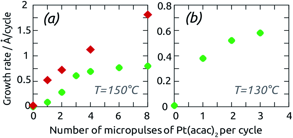 | ||
| Fig. 1 Growth rates determined at 150 °C (a) and at 130 °C (b) as a function of the Pt(acac)2 dosage by GCM for depositions using short 1 to 8 s (green) and long 30 s (red) exposure durations. The former give rise to self-limiting ALD behavior, the latter do not. | ||
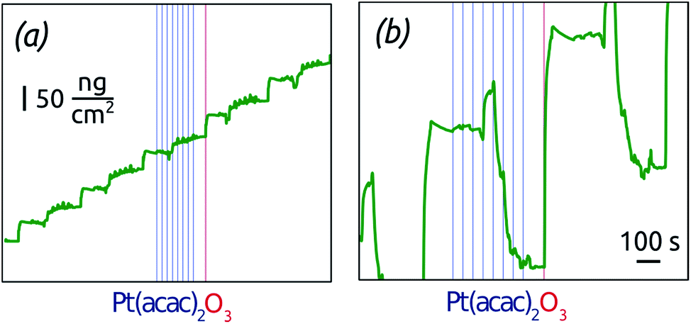 | ||
| Fig. 2 Mass evolution measured by piezoelectric crystal microbalance during Pt deposition carried out at 150 °C with 5 s (a) and 30 s (b) exposure duration. The light blue and red vertical lines highlight the pulses of Pt(acac)2 and ozone, respectively. The scales of the mass and time axes are identical in (a) and (b). | ||
The long exposure conditions (Fig. 2b) differ in that exposure to Pt(acac)2 results in large mass variations, and in an overall mass loss. Given that mass increases overall, Pt uptake from the gaseous precursor must be correlated with the loss of oxygen from the solid by decomposition of the platinum oxide to the metallic state. The absolute mass loss at this stage exceeds the mass gain over each cycle, therefore it cannot be due to combustion of the ligands alone. This indicates a ‘deep’ oxidation of the Pt surface to a metastable oxide, followed by its decomposition triggered by the Pt(acac)2 – again a precedented phenomenon.46,50–54
In other words, the ‘short exposure’ conditions do not leave sufficient time for the alternating transformations of the film between metallic and oxidic beyond the topmost layer, so that a well-behaved ALD growth ensues. In the ‘long exposure’ conditions, the film oscillates between states in which it is metallic and oxidic. In this case, the amount of reactive oxide, capable of immobilizing Pt(acac)2, is not under experimental control, which results in non-ALD growth. Note that this mechanism of non-self-limiting growth is fundamentally distinct from the simple thermal decomposition of the metal–organic precursor. In fact, we can exclude the thermal decomposition of Pt(acac)2 in these conditions by a control experiment conducted in the absence of O3, which yielded no growth.
The two contrasting cases of Fig. 2a and b are close to each other, as demonstrated by the GCM data recorded during nucleation in the ‘short exposure’ case, Fig. 3. During the first approximately 30 cycles in the ALD conditions, mass oscillations are observed reminiscent of those that prevail in the non-self-limited conditions. The growth then slowly reaches the well-behaved steady state. Such a nucleation stage is often observed when elemental metals are grown on oxide surfaces.55 The transition to steady-state growth can be associated with coalescence of the isolated nuclei to a continuous, more thermodynamically stable, film. This effect has been demonstrated previously.38
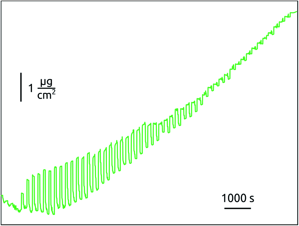 | ||
| Fig. 3 Mass evolution measured by piezoelectric crystal microbalance during the first 65 ALD cycles of Pt carried out at 150 °C with 5 s exposure duration. | ||
At a deposition temperature of 130 °C, mass fluctuations are consistently observed at all exposure durations (Fig. 4), but with a smaller absolute amplitude. We interpret this observation as indicating the formation upon O3 reaction of an oxide species exclusively confined to the surface, which then reacts with a limited amount of Pt(acac)2 in a fast manner.
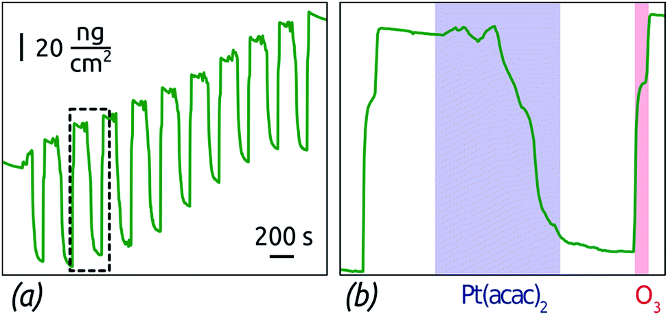 | ||
| Fig. 4 Mass evolution measured by piezoelectric crystal microbalance during Pt deposition carried out at 130 °C. (a) Overall mass evolution, (b) enlarged view over one ALD cycle. | ||
The ALD reaction between Pt(acac)2 and ozone enables us to coat deep pores conformally in both sets of self-limiting conditions defined above. Fig. 5 shows SEM micrographs of a Pt deposit performed at 130 °C on anodic alumina (AAO) membranes featuring parallel pores of 200 nm diameter. The close-up view (Fig. 5a) shows near the opening of the pores that the Pt deposit is continuous but with a significant roughness. The low-magnification cross-section (Fig. 5b) demonstrates a conformal Pt deposit over 25 μm long pores (aspect ratio >100).
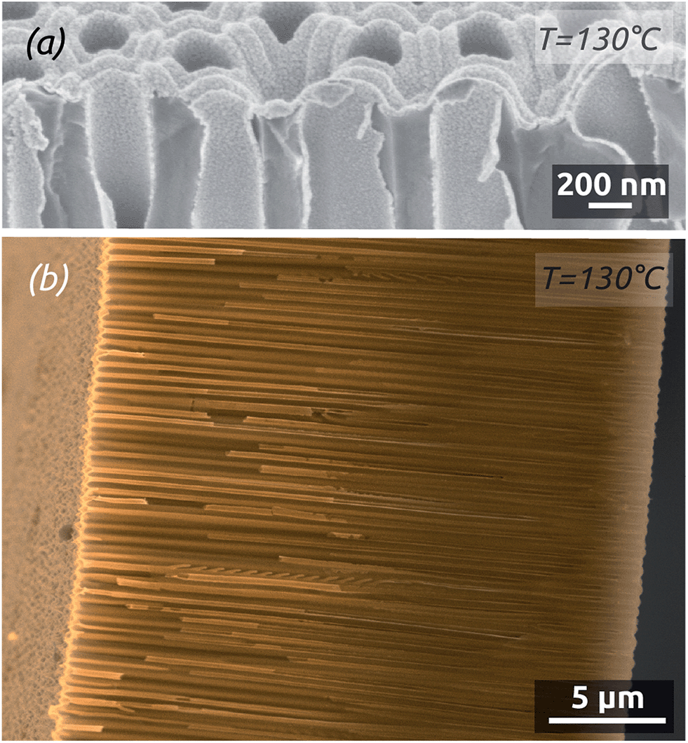 | ||
| Fig. 5 (a) Close-up view of the AAO pores mouth coated by a continuous layer of Pt clusters grown at 130 °C. (b) Cross section view of AAO pores filled with Pt deposited by ALD. The back-scattered electron signal is colored in sepia tone to highlight Pt on the alumina background (the secondary electron signal is in white). Continuous Pt tubes in light tone can be followed (either complete and convex or broken in halves and hollow) from one extremity of the otherwise dark pores to the other. | ||
Depositions carried out at 150 °C using short metal exposure durations yield films with a larger roughness and the thickness of which decreases over depth in the pores, so that coating is limited to an aspect ratio of 50 (Fig. 6). Note that in freestanding membranes (with the barrier oxide layer removed), precursors can access more easily from both sides of the membrane, resulting in even coating at an aspect ratio of 70.
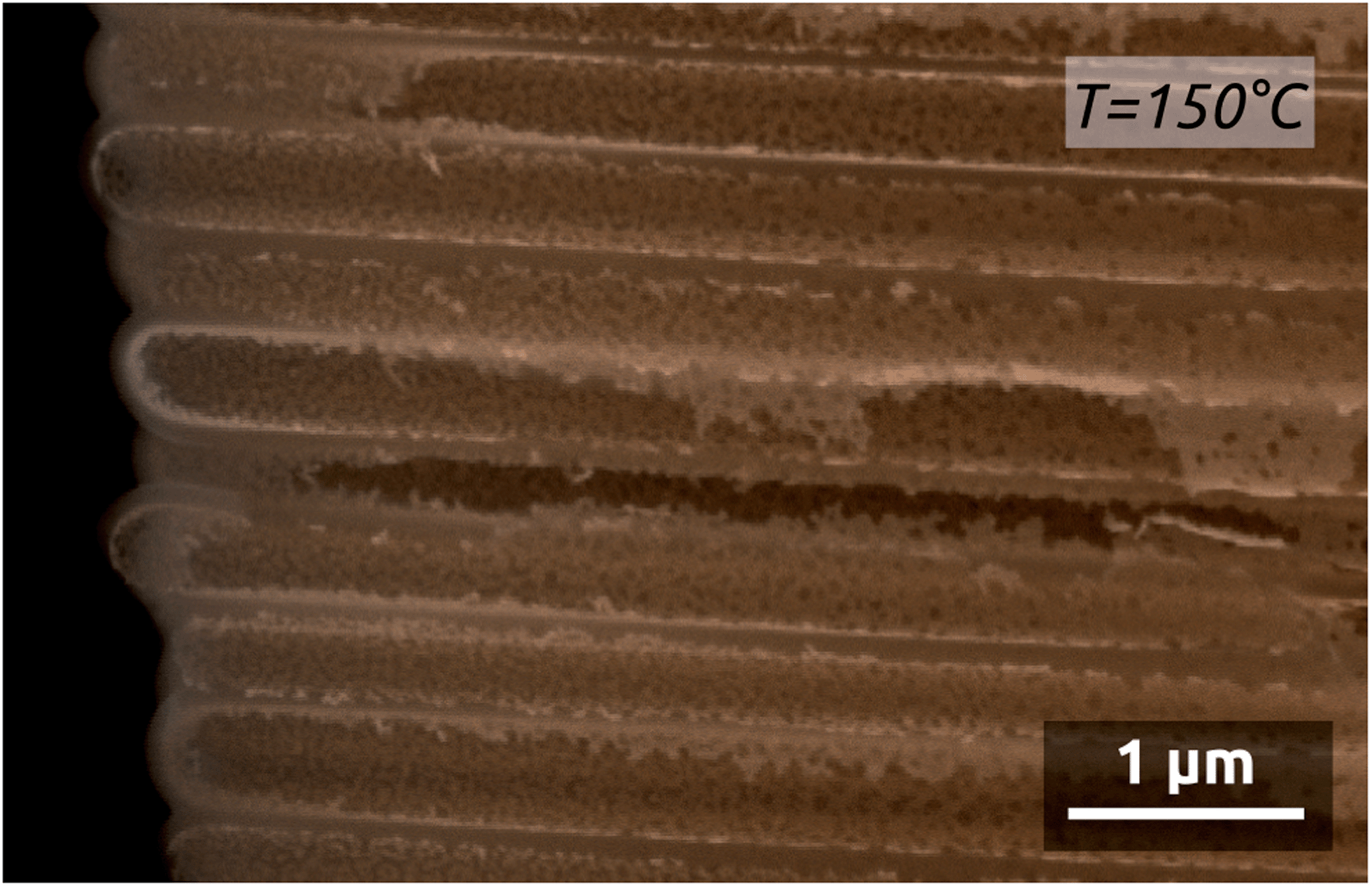 | ||
| Fig. 6 SEM micrograph of AAO membrane coated by Pt deposited by ALD at 150 °C. | ||
The crystalline structure of Pt films supported on AAO membranes was analyzed by X-ray diffraction. The diffractograms for both films grown at 150 °C and 130 °C are shown on Fig. 7. The three peaks located at 2θ values of 40.0°, 46.4° and 67.7° can be assigned to the [111], [200] and [220] reflexes of the fcc Pt lattice. This polycrystalline structure of Pt is likely the cause of the observed film roughness. Note that no crystalline platinum oxide is evident. Furthermore, no shift of the peaks with respect to the pure metallic reference (possibly due to incorporation of oxidized species) is apparent.56
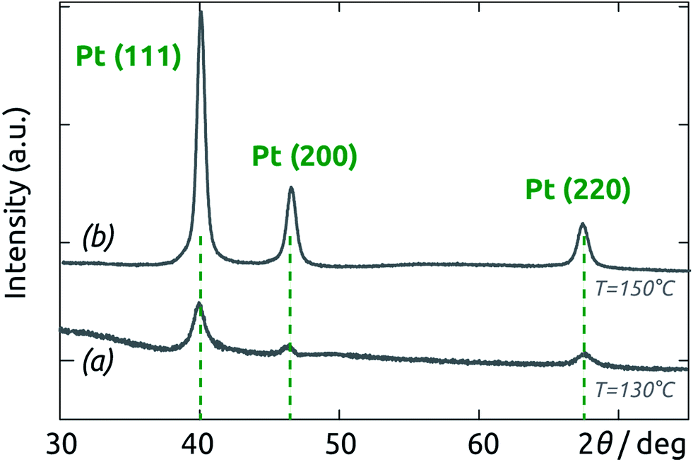 | ||
| Fig. 7 X-ray diffractograms of Pt deposited on AAO membranes by ALD at 130 °C (a) and 150 °C (b). | ||
3.2 Electrocatalytic activity of a model Pt/TiO2 nanotube system
Applying our nanoporous Pt system to electrocatalysis entails the use of an electrically conducting substrate. We choose anodic TiO2 tube arrays for this purpose. Fig. 8a shows the TiO2 nanotubes grown in an aqueous fluorine-containing electrolyte using literature procedures.28 The diameter of the pores is about 70 nm and the length approximately 500 nm for 1 h of anodization at 20 V. An annealing is performed for 2 h at 450 °C in air in order to crystallize TiO2 in the anatase phase. This improves the electrical conductivity of the material as well as its subsequent interaction with the metallic catalyst.29 The nanotubes are then functionalized by depositing a conformal layer of Pt clusters by ALD at 130 °C using the parameters described above. The thickness of the deposit is on the order of 10 nm (on each side of the TiO2 tube wall), as depicted on Fig. 8b (see also ESI Fig. S1†). This value obtained for 100 ALD cycles is compatible with the growth rate determined above.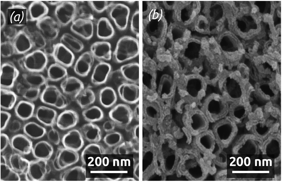 | ||
| Fig. 8 TiO2 nanotubes (a) as grown by anodic oxidation and (b) functionalized with Pt clusters. | ||
The presence of Pt in the nanoporous samples is confirmed by energy-dispersive X-ray spectroscopic chemical microanalysis (peaks at 2.0, 9.5 and 11.0 keV in Fig. 9a). The X-ray diffractogram of the resulting Pt/TiO2 system (Fig. 9b) shows that the new substrate does not influence the polycrystalline nature of the Pt deposit. Peaks at 40.0°, 46.4° and 67.7° correspond to the [111], [200] and [220] fcc Pt reflexes. Moreover, the peak at about 26° corresponds to the anatase phase of the crystalline TiO2 tubes, whereas the metallic Ti substrate gives rise to recognizable sharp peaks.
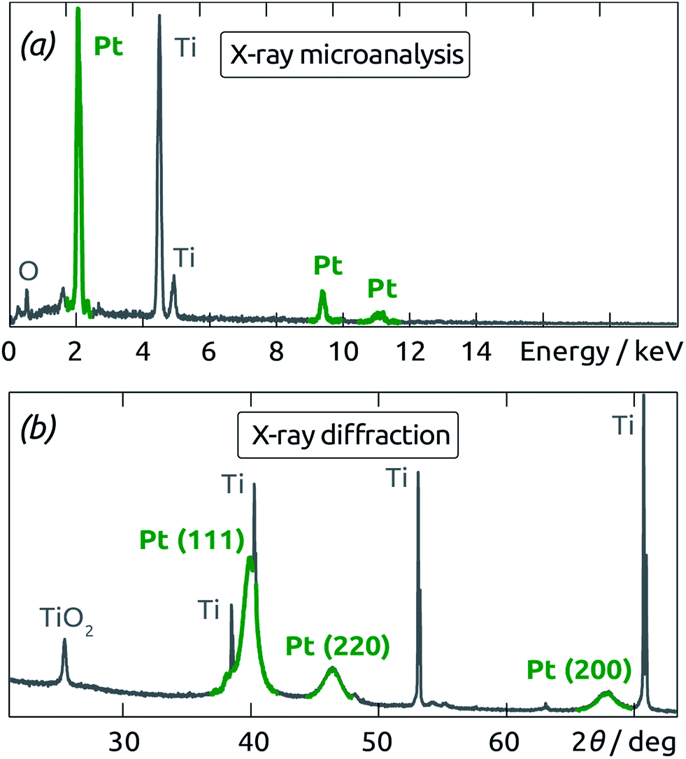 | ||
| Fig. 9 (a) Energy-dispersive X-ray spectroscopy analysis and (b) X-ray diffractogram performed on Pt deposited by ALD on annealed TiO2 nanotubes. | ||
The electrochemical characteristics of our Pt/TiO2 nanotubular samples are qualitatively similar to those of planar systems,57 as investigated by cyclic voltammetry. Starting from the open-circuit potential (OCP) measured at +0.05 V (vs. Ag/AgCl), the cyclic voltammogram (CV) recorded in aqueous acidic medium (0.5 M H2SO4, Fig. 10a) shows two reduction peaks located at −0.10 V and −0.19 V on the cathodic scan (with corresponding oxidation maxima at −0.08 V and −0.14 V). They correspond to the reductive adsorption of protons as hydrogen adatoms on the Pt surface. At −0.27 V, bulk dihydrogen evolution sets on. This shape of the cyclic voltammogram is fully consistent with reports of planar Pt electrodes in the literature.57
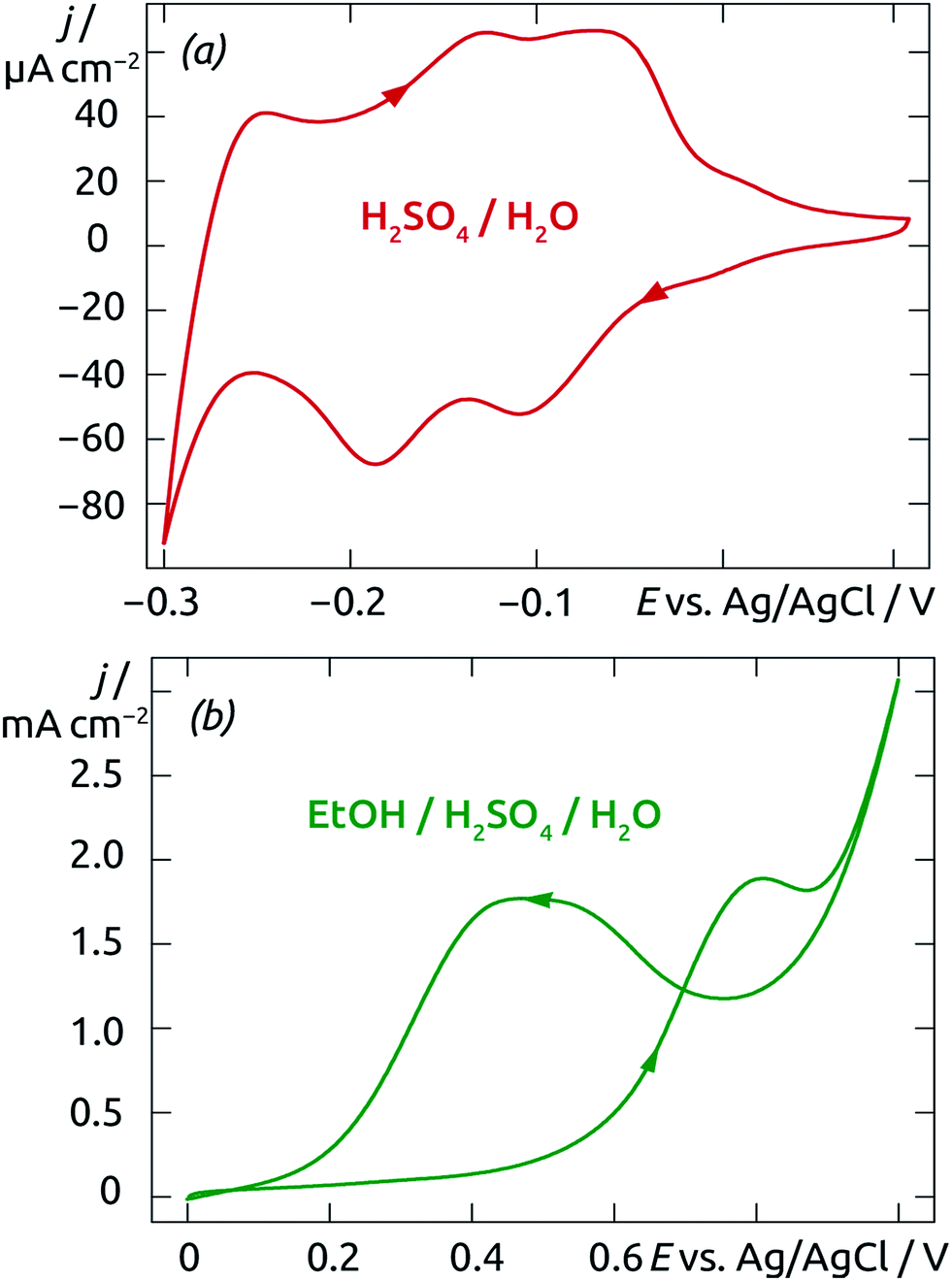 | ||
| Fig. 10 Cyclic voltammograms of Pt clusters supported on TiO2 nanotubes carried out in acidic medium (0.5 M H2SO4 (a), and 0.5 M H2SO4 + 1 M EtOH (b)). Scan rate: 50 mV s−1. | ||
The same conclusion is reached when ethanol (1 M) is added to the mixture. The resulting CV curve (Fig. 10b) displays an oxidation onset at +0.40 V, an anodic maximum at 0.68 V, followed by a new anodic maximum on the reverse scan. This behavior, which is characteristic of CO poisoning and subsequent surface reactivation, is again known for the planar Pt system.57
The curves recorded in basic conditions (Fig. 11) display very similar features, shifted along the potential axis due to the difference in pH. Once again, the surface electrochemistry of our nanotubular Pt/TiO2 system conforms to that known for pure, planar Pt.
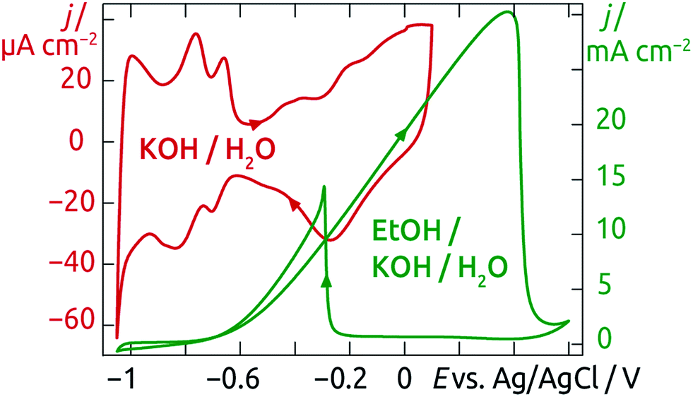 | ||
| Fig. 11 Cyclic voltammograms of Pt clusters supported on TiO2 nanotubes carried out in 1 M KOH and in 1 M KOH + 1 M EtOH. Scan rate: 50 mV s−1. | ||
Although the curves qualitatively conform to the known planar case, they differ from it in a quantitative sense. Indeed, the current densities obtained are significantly higher, up to tens of mA cm−2. Taking into account the geometry of the samples, this corresponds to a specific current on the order of 50 mA (mg Pt)−1, comparable to the state of the art.58 This highly efficient utilization of the noble metal catalysts suggests that our preparative method might be of interest in electrochemical energy conversion applications.
3.3 Electrocatalytic activity of a Pt/TiO2/Ti felt system
Electrocatalysis applications such as fuel cells and electrolyzers typically rely on electrically conductive fleeces or felts as electrode substrates instead of planar foils. Graphite and titanium are the two most prominently used materials for this purpose, which withstand the corrosive conditions. Transferring our preparative procedure described above to such a felt implies anodizing it as the first step. This has not been reported to date. Applying 40 V to such a commercially available Ti fleece (shown in Fig. 12a) for 2 h in a 0.5 wt% NH4F solution in glycerol as the solvent results in the formation of a well-defined nanoporous TiO2 layer,25 as documented by the SEM micrographs, Fig. 12b–d. The cross-section views (Fig. 12b and c) show the resulting narrow tubes with a length of about 1.5 μm and a diameter of 20 nm. The lower extremity of the tubes (Fig. 12d) exhibits the typical ‘barrier’ layer of oxide in contact with the underlying metal. Care must be taken to rinse the anodized sample exhaustively after the anodic treatment in order to prevent that the nanoporous TiO2 layer be covered by a dense continuous oxide film (see ESI Fig. S2†).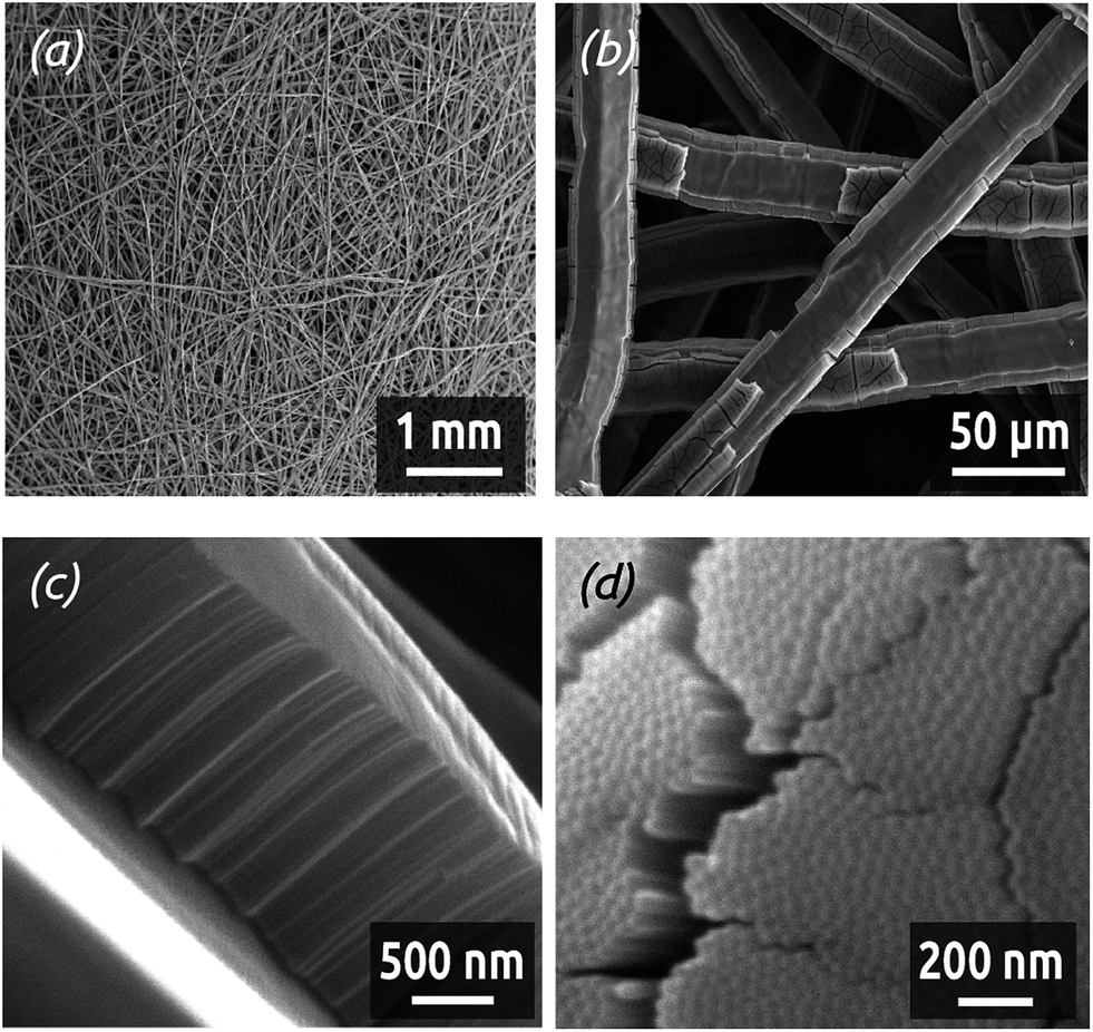 | ||
| Fig. 12 SEM micrographs of Ti fleeces before anodization (a) and after anodization (glycerol + 0.5 wt% NH4F, 40 V, 2 h, (b and c)). The lower extremity of TiO2 tubes in an oxide block separated from the underlying Ti is shown in (d). An ultrasonication treatment has been performed before SEM observation in order to provide insight into the otherwise solid oxide layer. | ||
The anodized felts are subsequently coated by a thin (5 nm) catalytic layer of Pt by ALD carried out at 130 °C using the parameters described above. For comparison purposes, other anodized felts were submitted to a deposition of 10 nm Pt by magnetron sputtering. The comparison of the electrocatalytic activity (in a 1 M H2SO4 solution) of Ti felts submitted to various treatments is shown on Fig. 13. The potentials are measured with respect to an Ag/AgCl reference electrode. Starting from the open circuit potential measured at about +0.6 V, the potentials are at first swept anodically up to +1.65 V, after which the CV is continued down to −0.45 V (at 100 mV s−1). For Ti felts without any electrochemical treatment nor Pt layer, the current density remains low (below 2 mA cm−2 in absolute value), no electrochemical activity is observed (gray curve). Providing a larger specific surface area by anodizing the Ti felts for 2 h (blue curve) increases the current somewhat, especially in the H2 evolution region (the most cathodic potentials). However, the absolute current density remains low, a few microamperes per cm2 of felt (measured macroscopically), due to the absence of an appropriate catalyst.
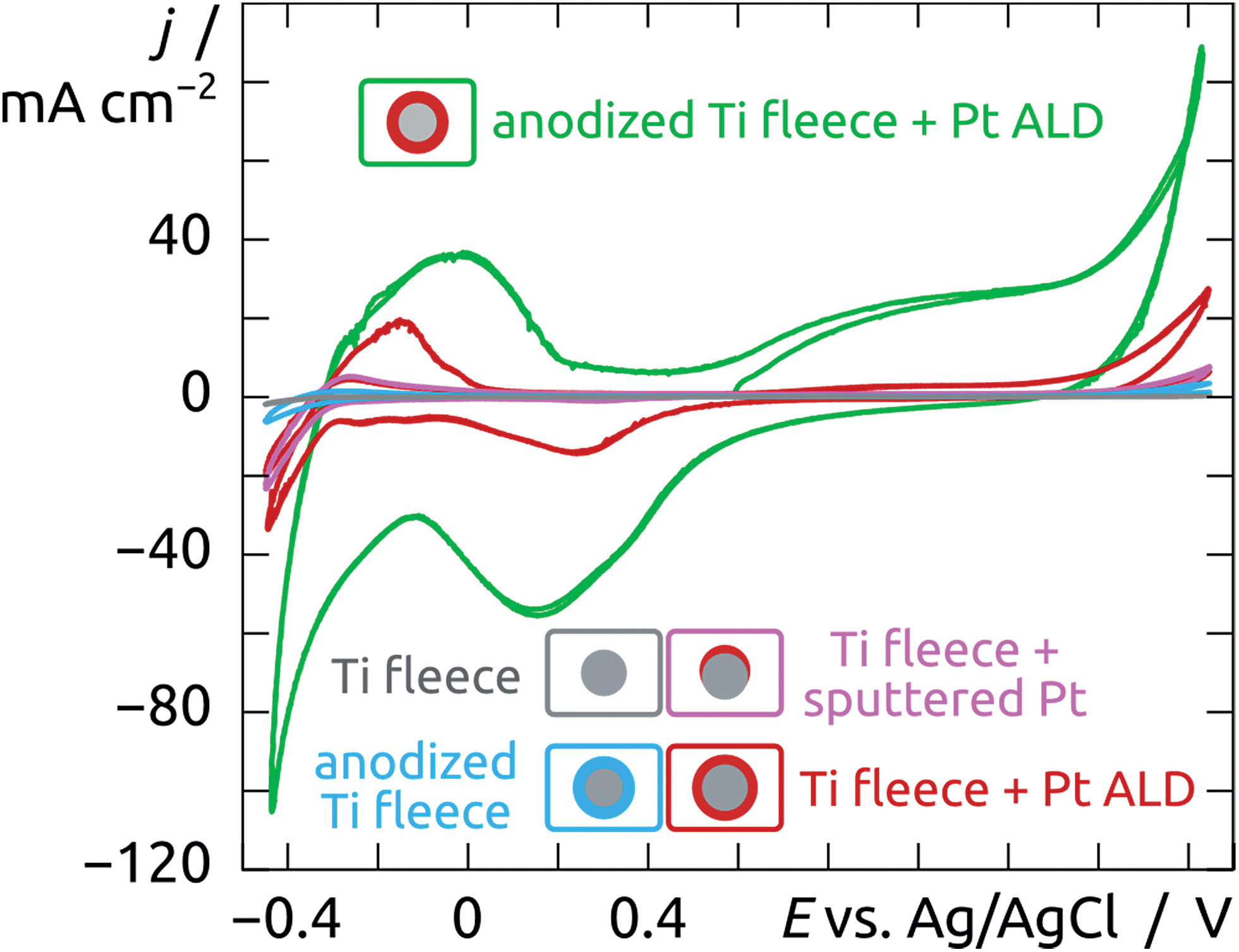 | ||
| Fig. 13 Cyclic voltammetry performed on Ti fleeces under different conditions with and without Pt. Ti fleeces have been anodized and Pt has been deposited either by magnetron sputtering or by ALD. Scan rate: 100 mV s−1. Internal resistance compensation was performed. | ||
Deposition of 10 nm Pt by magnetron sputtering on the commercial Ti felts causes a significant increase in electrolytic current density (pink curve), reaching maximum current densities of −20 mA cm−2 and 5 mA cm−2 at −0.45 V and +1.65 V, respectively. These values remain quite modest for a felt (as opposed to a foil). Indeed, magnetron sputtering has limited ability to coat non-planar substrates. Being a directional deposition method, it only generates a film on the uppermost surfaces of the felt instead of coating each fiber. The ALD technique provides precisely the advantage of conformal coating. Depositing 5 nm of Pt by ALD, one obtains yet a further increase in current density (red curve) with respect to the sputter-coated sample. Moreover, the curve shape is now clearly reminiscent of that known for platinum (Fig. 11), with the anodic formation of surface hydroxide and oxide at positive potentials and the cathodic generation of surface hydrides in the negative potential region. In the bulk H2 generation regime, for potentials below −0.3 V, the current density reaches −35 mA cm−2 at −0.45 V.
Finally, we consider a Ti felt combining all favorable treatments: anodization (2 h) for the large surface area, followed by ALD coating with 5 nm Pt for catalytic proficiency. The result, shown as the green curve of Fig. 13, is quite dramatic. The qualitative curve shape of a Pt surface is clearly recognizable, but the quantitative values of the current density are very high. Both extremities of the cyclic voltammogram (in the bulk hydrogen and oxygen evolution regions) reach current densities on the order of 100 mA cm−2. This represents an enhancement by a factor >50 with respect to the naked, commercial Ti felt. Much of the success of our preparative strategy is attributable to the generation of a large surface area. The catalytically active Pt surface area can be evaluated by integrating the hydride generation current and comparing it to the established value of 0.21 mC cm−2 of planar Pt.59 This approach delivers a roughness factor (microscopic catalytically active surface area over macroscopically defined sample area) of approximately 300. This experimentally derived area combined with the known nominal Pt film thickness also yields an upper bound for the Pt loading of 3 mg cm−2 felt (value calculated for a hypothetically smooth film). Taking into account film roughness would yield lower loading values. Thus, the electrocatalytic water reduction efficiency is on the order of 30 mA (mg Pt)−1 at −0.45 V or better. Note that the capacitive contribution to the current measured at this potential is insignificant, as indicated by the light blue curve of Fig. 13. Also, the fact that the pink, red and green curves differ drastically in magnitude without large shifts of the peaks demonstrates that the ohmic resistance of the TiO2 material is low. This puts our ALD-based system on par with the state of the art,58 and leaves some room for improvement as the ALD method enables us to lower the Pt loading quite systematically in the future.
4. Conclusions
This study establishes a link between fundamental surface reactivity, thin film deposition, preparation of nanostructured noble metal surfaces, and electrocatalytic application. The mechanism of the atomic layer deposition reaction between Pt(acac)2 and O3 is shown to involve an oxidation of the metallic surface which, depending on the conditions, can affect more than the topmost atomic layer. This behavior, which has been documented in the surface science and catalysis communities, and was shown to prevail in the ALD of platinum using the (MeCp)PtMe3 precursor, is found to be similar when using Pt(acac)2. In essence, deep oxidation of the metallic film and abrupt decomposition of the oxide are inherent properties of platinum. In other words, they will take place independently of the exact metal–organic precursor used. Thus, controlling the film oxidation and the subsequent thermal decomposition of the oxide is crucial to the definition of a self-limiting deposition procedure (ALD behavior). Using adequate experimental parameters, this ALD process yields excellent coverage of high aspect ratio nanopores with metallic Pt. Different electrochemically grown nanoporous oxide substrates are applicable to this ALD procedure, derived either from foils (anodized Al and Ti) or from three-dimensional structures (anodized Ti felts). After Pt ALD coating, the TiO2-based systems are electrochemically active in a way that qualitatively conforms to established knowledge of the electrocatalytic Pt system. Current densities are large due to the high specific surface area of the nanoporous substrate. Pt utilization is efficient, as an excellent film thickness control is achievable by ALD. Further steps towards real-world application of this system in fuel cells include a further lowering of the noble metal loading and the investigation of ALD coatings on alternative substrates. These goals are within reach by ALD, which additionally features the industrial advantage of being a solventless method, in which a very large fraction (potentially >90%) of the precursor material is found in the deposited film.The method established here is quite general, and is applicable to various noble metals and various electrochemical applications. Based on it, further development is possible by exploitation of binary or ternary catalytic materials based for example on the combination of platinum and iridium, in elemental and/or oxidized form. Such systems, which can be obtained by ALD, are well established as reversible fuel cell electrode catalysts with properties that can be optimized in terms of chemical stability and electrocatalytic throughput.60–63
Acknowledgements
The authors gratefully acknowledge Prof. W. Peukert and S. Romeis (FAU Chemical Engineering) for access to XRD facility and E. Butzen (MPI for the Science of Light) for his support with SEM. We thank the company Bekaert for graciously providing Ti felts for our research. This work is funded by the Cluster of Excellence ‘Engineering of Advanced Materials’, and the project ‘tubulAir±’ (project number 03SF0436 G) supported by the Bundesministerium für Bildung und Forschung. SB was supported by the European Community's Seventh Framework program under grant agreement 312284.References
- A. S. Aricò, P. Bruce, B. Scrosati, J.-M. Tarascon and W. van Schalkwijk, Nat. Mater., 2005, 4, 366 CrossRef PubMed.
- C. Liu, F. Li, L.-P. Ma and H.-M. Chen, Adv. Mater., 2010, 22, E28 CrossRef CAS PubMed.
- H. Wedemeyer, J. Michels, R. Chmielowski, S. Bourdais, M. Sugiura, G. Dennler and J. Bachmann, Energy Environ. Sci., 2013, 6, 67 Search PubMed.
- T. Grünzel, Y. J. Lee, K. Kueppel and J. Bachmann, Beilstein J. Nanotechnol., 2013, 4, 655 CrossRef PubMed.
- S. Park, Y. Shao, J. Liu and Y. Wang, Energy Environ. Sci., 2012, 5, 9331 Search PubMed.
- C. Lamy, A. Lima and V. Le Rhun, J. Power Sources, 2002, 105, 283 CrossRef CAS.
- S. H. Joo, S. J. Choi, I. Oh, J. Kwak, Z. Liu, O. Terasaki and R. Ryoo, Nature, 2001, 412, 169 CrossRef CAS PubMed.
- Y.-G. Guo, J.-S. Hu and L.-J. Wan, Adv. Mater., 2008, 20, 2878 CrossRef CAS.
- W. Li, C. Liang, W. Zhou, J. Qiu, Z. Zhou, G. Sun and Q. J. Xin, J. Phys. Chem. B, 2003, 107, 6292 CrossRef CAS.
- P. Forrer, F. Schlottig, H. Siegenthaler and M. Textor, J. Appl. Electrochem., 2000, 30, 533 CrossRef CAS.
- V. Roscher, M. Licklederer, J. Schumacher, G. Reyes Rios, B. Hoffmann, S. Christiansen and J. Bachmann, Dalton Trans., 2014, 43, 4345 RSC.
- J. Gemmer, Y. Hinrichsen, A. Abel and J. Bachmann, J. Catal., 2012, 290, 220 CrossRef CAS.
- K. Scott, W. M. Taama and P. Argyropoulos, J. Power Sources, 1999, 79, 43 CrossRef CAS.
- H. Liu, C. Song, L. Zhang, J. Zhang, H. Wang and D. P. Wilkinson, J. Power Sources, 2006, 155, 95 CrossRef CAS.
- W. S. Baker and R. M. Crooks, J. Phys. Chem. B, 1998, 102, 10041 CrossRef CAS.
- J. C. Hulteen, V. P. Menon and C. R. Martin, J. Chem. Soc., Faraday Trans., 1996, 92, 4029 RSC.
- V. P. Menon and C. R. Martin, Anal. Chem., 1995, 67, 1920 CrossRef CAS.
- R. W. Murray, Chem. Rev., 2008, 108, 2688 CrossRef CAS PubMed.
- L. Assaud, E. Monyoncho, K. Pitzschel, A. Allagui, M. Petit, M. Hanbücken, E. A. Baranova and L. Santinacci, Beilstein J. Nanotechnol., 2014, 5, 162 CrossRef PubMed.
- R. Prehn, L. Abad, D. Sanchez-Molas, M. Duch, N. Sabate, F. J. Del Campo, F. X. Munoz and R. G. Compton, J. Electroanal. Chem., 2011, 662, 361 CrossRef CAS.
- I. Streeter, N. Fietkau, J. Del Campo, R. Mas, F. X. Munoz and R. G. Compton, J. Phys. Chem. C, 2007, 111, 12058 CrossRef CAS.
- H. Masuda, H. Tanaka and N. Baba, Chem. Lett., 1990, 4, 621 CrossRef.
- K. Nielsch, J. Choi, K. Schwirn, R. B. Wehrspohn and U. Gösele, Nano Lett., 2002, 2, 677 CrossRef CAS.
- J. M. Macak, H. Tsuchiya and P. Schmuki, Angew. Chem., Int. Ed., 2005, 44, 2100 CrossRef CAS PubMed.
- J. M. Macak, H. Tsuchiya, L. Taveira, S. Aldabergerova and P. Schmuki, Angew. Chem., Int. Ed., 2005, 44, 7463 CrossRef CAS PubMed.
- J. M. Macak, H. Tsuchiya, A. Ghicov, K. Yasuda, R. Hahn, S. Bauer and P. Schmuki, Curr. Opin. Solid State Mater. Sci., 2007, 11, 3 CrossRef CAS.
- P. Roy, S. Berger and P. Schmuki, Angew. Chem., Int. Ed., 2011, 50, 2904 CrossRef CAS PubMed.
- L. Assaud, V. Heresanu, M. Hanbücken and L. Santinacci, C. R. Chim., 2013, 16, 89 CrossRef CAS.
- X.-M. Wang and Y.-Y. Xia, Electrochim. Acta, 2010, 55, 851 CrossRef CAS.
- P. Forrer, F. Schlottig, H. Siegenthaler and M. Textor, J. Appl. Electrochem., 2000, 30, 533 CrossRef CAS.
- L. Philippe and J. Michler, Small, 2008, 4, 904 CrossRef CAS PubMed.
- J. W. Elam, D. Routkevitch, P. P. Mardilovich and S. M. George, Chem. Mater., 2003, 15, 3507 CrossRef CAS.
- J. Bachmann, J. Jing, M. Knez, S. Barth, H. Shen, S. Mathur, U. Gösele and K. Nielsch, J. Am. Chem. Soc., 2007, 129, 9554 CrossRef CAS PubMed.
- N. S. Porter, H. Wu, Z. Quan and J. Fang, Acc. Chem. Res., 2013, 46, 1867 CrossRef CAS PubMed.
- J. Bachmann, R. Zierold, Y. T. Chong, R. Hauert, C. Sturm, R. Schmidt-Grund, B. Rheinländer, M. Grundmann, U. Gösele and K. Nielsch, Angew. Chem., Int. Ed., 2008, 47, 6177 CrossRef CAS PubMed.
- Y. T. Chong, E. M. N. Yau, K. Nielsch and J. Bachmann, Chem. Mater., 2010, 22, 6506 CrossRef CAS.
- E. Moyen, L. Santinacci, L. Masson, H. Sahaf, M. Macé, L. Assaud and M. Hanbücken, Int. J. Nanotechnol., 2012, 9, 246 CrossRef CAS.
- J. Hämäläinen, F. Munnik, M. Ritala and M. Leskelä, Chem. Mater., 2008, 20, 6840 CrossRef.
- T. Aaltonen, M. Ritala, T. Sajavaara, J. Keinonen and M. Leskelä, Chem. Mater., 2003, 15, 1924 CrossRef CAS.
- R. L. Puurunen, J. Appl. Phys., 2005, 97, 121301 CrossRef.
- S. M. George, Chem. Rev., 2010, 110, 111 CrossRef CAS PubMed.
- J. W. Elam, D. Routkevitch, P. P. Mardilovich and S. M. George, Chem. Mater., 2003, 15, 3507 CrossRef CAS.
- J. A. McCormick, K. P. Rice, D. F. Paul, A. W. Weimer and S. M. George, Chem. Vap. Deposition, 2007, 13, 491 CrossRef.
- B. B. Burton, M. P. Boleslawski, A. T. Desombre and S. M. George, Chem. Mater., 2008, 20, 7031 CrossRef CAS.
- Y. Du, X. Du and S. M. George, Thin Solid Films, 2005, 491, 43 CrossRef CAS.
- H. Thanner, P. W. Krempl, W. Wallnöfer and P. M. Worsch, Vacuum, 2002, 67, 687 CrossRef CAS.
- W. M. M. Kessels, H. C. M. Knoops, S. A. F. Dielissen, A. J. M. Mackus and M. C. M. Van de Sanden, Appl. Phys. Lett., 2009, 95, 013114 CrossRef.
- S. T. Christensen and J. W. Elam, Chem. Mater., 2010, 22, 2517 CrossRef CAS.
- T. Aaltonen, A. Rahtu, M. Ritala and M. Leskelä, Electrochem. Solid-State Lett., 2003, 6, C130 CrossRef CAS.
- N. A. Saliba, Y.-L. Tsai, C. Panja and B. E. Koel, Surf. Sci., 1999, 419, 79 CrossRef CAS.
- W. X. Li, L. Österlund, E. K. Vestergaard, R. T. Vang, J. Matthiesen, T. M. Pedersen, E. Laegsgaard, B. Hammer and F. Besenbacher, Phys. Rev. Lett., 2004, 93, 146104 CrossRef CAS PubMed.
- J. F. Weaver, J.-J. Chen and A. L. Gerrard, Surf. Sci., 2005, 592, 83 CrossRef CAS.
- A. J. M. Mackus, N. Leick, L. Baker and W. M. M. Kessels, Chem. Mater., 2012, 24, 1752 CrossRef CAS.
- W. Setthapun, W. D. Williams, S. Min Kim, H. Feng, J. W. Elam, F. A. Rabuffetti, K. R. Poeppelmeier, P. C. Stair, E. A. Stach, F. H. Ribeiro, J. T. Miller and C. L. Marshall, J. Phys. Chem. C, 2010, 114, 9758 CrossRef CAS.
- V. Miikkulainen, M. Leskelä, M. Ritala and R. L. Puurunen, J. Appl. Phys., 2013, 113, 021301 CrossRef.
- M. Ammam and E. B. Easton, J. Power Sources, 2012, 215, 188 CrossRef CAS.
- R. Manoharan and J. B. Goodenough, J. Mater. Chem., 1992, 2, 875 RSC.
- H. Hua, C. Hu, Z. Zhao, H. Liu, X. Xie and Y. Xi, Electrochim. Acta, 2013, 105, 130 CrossRef CAS.
- S. Trasatti and O. A. J. Petrii, Electroanal. Chem., 1992, 321, 353 CrossRef.
- J. Hämäläinen, M. Kemell, F. Munnik, U. Kreissig, M. Ritala and M. Leskelä, Chem. Mater., 2008, 20, 2903 CrossRef.
- T. Aaltonen, M. Ritala, V. Sammelselg and M. Leskelä, J. Electrochem. Soc., 2004, 151, G489 CrossRef CAS.
- J. Pettersson, B. Ramsey and D. Harrison, J. Power Sources, 2006, 157, 28 CrossRef CAS.
- S. T. Christensen and J. W. Elam, Chem. Mater., 2010, 22, 25 CrossRef.
Footnotes |
| † Electronic supplementary information (ESI) available. See DOI: 10.1039/c5ta00205b |
| ‡ Current address: University of Toulouse, Laboratory of Chemical Engineering, ENSIACET/INP Toulouse/UMR CNRS 5503, 4 allée Émile Monso, BP 44362, 31432 Toulouse Cedex 4, France. |
| § Current address: University of Göttingen, Institute for Organic and Biomolecular Chemistry, Tammannstr. 2, 37077 Göttingen, Germany. |
| This journal is © The Royal Society of Chemistry 2015 |